Note: The speaker is too small to reproduce lower frequency sounds unaided, but the addition of a baffle of
some kind improves it considerably. Given the layout of the PCB, the simplest baffle you can make is a small
paper cone (25 to 50mm long), with some Blutak or similar to seal the narrow end to the speaker. The
bigger the baffle the better the low frequency sound will be.
Power Suppl
Caution! Suppl this board with 12VDC, unless ou know that attached subs stems (such as a
Displa Adaptor/Displa Backlight) are compatible with a different suppl voltage.
The board may be powered from a supply voltage range of less than 7.5V, up to 28 volts unregulated DC.
The current consumption depends on the input voltage, what is attached to the unit and whether the
processor is idle, but power consumption is usually around 1 Watt when the VM2 is idle and with no external
devices attached or subsystems configured, and perhaps 3 - 4 Watts with a typical configuration including
graphics display.
The board has two regulators - a switch mode regulator to generate a 5V supply, and then a linear regulator
to drop the 5V to 3.3V.
The main (switch mode) regulator is efficient over a wide input voltage range. There is a silicon diode before
the regulator to protect against reverse polarity on the supply input.
Power Connector
2 way pluggable screw terminal. Plug provided.
Breakout connectors
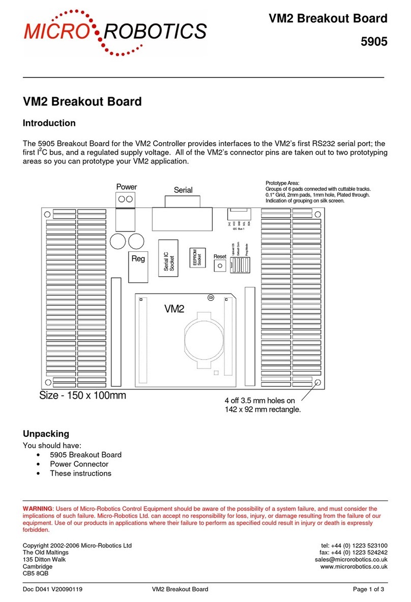
The two breakout connector positions are provided at each end of the VM2, labelled BRK1 and BRK2. These
are two sets of pads that exactly reproduce the connectors on the VM2, but on a 0.1” pitch. Note that the
VCC and GND pads are marked with + and – signs.
You should refer to the table of channel usage on page 9 and the circuit diagram of this board before using
the signals brought out here.
Table of links
This table details the function of each of the links on the board. The positions of all the links are shown on
the diagram of the board.
Link Open Link pins 1 & 2 Link pins 2 & 3
LK1 Chan $34 free Chan $34 used for Ethernet
interrupt.
LK2 U B pull up circuit not controlled U B pull up circuit controlled
by Dflt Comm signal
LK3 Chan $3B is free Chan $3B used for erial Port
4 RX.
LK4 R 485 not terminated R 485 terminated
LK5, LK6 R 485 not pulled to idle state R 485 pulled to idle state
LK7 CAN Bus not terminated CAN Bus terminated
LK8 CAN shield pin open CAN shield pin grounded
LK9 Alpha LCD back-light pin open Alpha LCD back-light
connected to Alpha LCD Vcc
LK10 I2C Bus not powered I2C Bus Vcc is 3.3V I2C Bus Vcc is 5V
LK11 Alpha LCD not powered Alpha LCD Vcc is 3.3V Alpha LCD Vcc is 5V
LK12 Back-light on/off signal open Backlight controlled by Chan
$26
Back-light controlled by
BacklightPWM signal
(VM2D2 / 5920 only)
LK13, LK14 CAN, USB not connected:
Chans $1B, $1C are free
CAN Tx, Rx connected: uses
Chans $1B and $1C
U B data connected:
uses Chans $1B and $1C
D050_5922_VM2_App_Board3 Page 8 of 11
