Application Note 1952
2AN1952.1
July 30, 2015
Submit Document Feedback
What is Inside
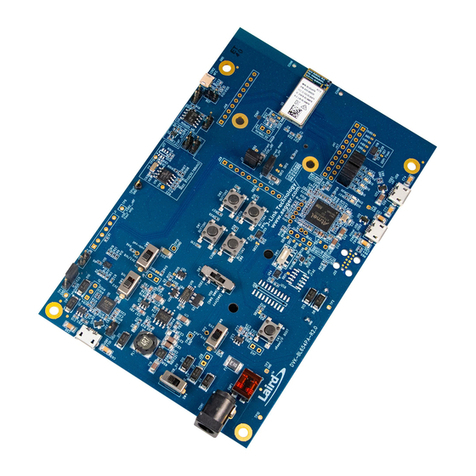
The Evaluation Kit contains:
• ISL94203 evaluation board
• MCB_PS_Z multicell power supply test board
• ISL94203INTFACEKIT1Z USB to I2C interface kit, includes a
PCB and I2C cable
• USB cable, connects PC to USB-I2C interface board
What is Needed
The following instruments will be needed to perform testing:
• 30V/1A adjustable power supply
• Wires to connect power supply to MCB_PS_Z board
• Precision multimeter (optional)
• Oscilloscope (optional)
• Cables and wires (optional)
Software Installation
Step 1: Connect the ISLUSBI2C USB to the PC. The board
should automatically enumerate in the device control
panel under Human Interface Devices. The vendor ID
will be 0x09AA and the product ID will be 0x2036.
Since it is a HID device, no special driver is needed.
Step 2: Copy the Intersil_ISL94203_Installer_Vxxx.exe
program to the PC (any desired location). Double-click
to run the installation file. Note you may need to use
the “Run as Administrator” open when performing the
installation.file.
Quick Hardware Setup Guide
Step 1: Check the jumpers and switches on the board. The
board should be configured as follows:
•ADDR jumper set to “0”.
•xT2 Select jumper on either “CELL” or “FET”.
• FET jumpers set for either one path or two path.
Start with one path.
•J4 jumper is set to “1 Path”.
J9 jumper is set to “1 Path”.
Step 2: Connect the power supply to the MCB_PS_Z board. The
positive terminal is J5/J11 and the negative terminal is
J8/J12. There should be a jumper on JP2/8CELL.
Step 3: Set the power supply voltage to 28V (3.5V per cell).
(Optional: check that the voltages at terminal J1 or J3
are 3.5V per cell).
Step 4: Turn off the power to the power supply.
Step 5: Connect the ISL94203 board directly to the MCB_PS_Z
board at connector J1. Make sure the board is
connected on the ground side of J1 (see Figure 2).
Step 6: Turn on the power to the supply. If no LEDs light, press
the “WakeUp” button. Notice that there is one green
LED (RGO), indicating the LDO regulator on the
ISL94203 is operating.
The voltages at various points should be:
RGO = 2.5V ±3%
VREF = 1.80V ±0.5%
Step 7: Connect the USB port of the PC to the USB port of the
ISL94203INTFACEKIT1Z interface board.
Step 8: Connect the I2C cable from the
ISL94203INTFACEKIT1Z board to the
ISL94203EVKIT1Z board (J13).
Step 9: Open the ISL94203 GUI software. Use the software to
read the cell voltages.
Step 10: Compare the voltages at the board input (use a meter
to measure each input voltage, because the MCB_PS_Z
board may not accurately divide the voltages into equal
3.5V steps) with the readings provided by the GUI.
These voltages should closely match.
Step 11: See other operations described later in this document.
PCB Layout Guidelines
The AC performance of this circuit depends greatly on the care
taken in designing the PC board. The following are
recommendations to achieve optimum high performance from
your PC board.
• The use of low inductance components, such as chip resistors
and chip capacitors, is strongly recommended.
• Minimize signal trace lengths. This is especially true for the
VDD, charge pump decoupling, CS1, CS2, and VC0-VC8 inputs.
Trace inductance and capacitance can easily affect circuit
performance. Vias in the signal lines add inductance at high
frequency and should be avoided.
• Match channel-to-channel analog I/O trace lengths and layout
symmetry. This is especially true for the CS1 and CS2 lines,
since their inputs are normally very low voltage.
• Maximize use of AC decoupled PCB layers. All signal I/O lines
should be routed over continuous ground planes (i.e., no split
planes or PCB gaps under these lines). Avoid vias in the signal
I/O lines.
• When testing, use good quality connectors and cables,
matching cable types and keeping cable lengths to a
minimum.
