manuals.online logo
Brands
  1. Home
  2. •
  3. Brands
  4. •
  5. Rohm
  6. •
  7. Microcontroller
  8. •
  9. Rohm BD91N01NUX Installation and operating instructions

Rohm BD91N01NUX Installation and operating instructions

1/10
© 2021 ROHM Co., Ltd.
No. 64AN082E Rev.001
Oct. 2021
Application Note
USB Type-C Sink Port Detection and Protection IC
BD91N01NUX Function Description
This product is a USB Type-C detection IC that is compatible with USB Type-C Rev2.1 standard for applications
which require to sink power. When a Type-C plug is inserted, the product enters stand-alone operation where it
supplies power from VBUS to the system. Through this product, a Type-C interface can be introduced to receive
voltage and current of up to 5V/3A which is the Type-C standard.
It can be used in applications that operate up to 15W of power, allowing the user to combine the ports of applications
that had separate traditional power like USB Standard/Micro/Mini B ports.
Specification Description
This product is dedicated for the Sink application. When
a Source device is connected via Type-C, a series of
operations are performed; the product operates through
the VBUS power, then detects the orientation of Type-
C, insertion and removal detection, then selects the
USB Type-C current. The connection status is relayed
to the system via output terminals. When a Type-C
connection is detected, the Pch-MOS FET in the VBUS
power line turns ON, supplying power to the system.
The status of the Type-C connection can be monitored
by checking each digital output using an MCU. Since the
product does not have an input setting terminal,
configuring the MCU is not required.
The Pch-MOS FET on the VBUS power line
automatically turns off when Source device is
disconnected.
[Power Supply Specification]
●VBUS =4.0 to 5.5V
●VDDIO =1.7 to 5.5V
[Type-C Connection specification]
●SNK / UFP
[SNK (Power Sink) Specification]
●Inform the system of the Type-C connection condition
via both TCC1 and TCC0.
[Protection Function specification]
●VBUS Over Voltage protection
●VBUS Under Voltage Lockout
[Digital Output terminals]
The following features are assigned to digital output
terminals.
Table 1. Digital output terminals
Terminal #
Name
Output
Voltage
Level
Features
6
TCC1
VDDIO
The 2-bit data of
Type-C current
capability
7
TCC0
VDDIO
8
ORIENT
VDDIO
Plug Orientation
9
SWMONI
VDDIO
Status of external
Pch-MOS FET
Note: All digital terminals have NO pull-down or pull-
up.
Unsupported Features
Table 2 lists the following features which the product
does not support since it only supports Type-C Sink
and UFP. Please check our USB PD controllers if the
following listed features are needed.
Table 2. Features not supported by BD91N01NUX
Unsupported features
OTG
Power Delivery
Dual Role Power Port
Power Role Swap
Dual Role Data Port
Data Role Swap
Source
PPS
DFP
Fast Role Swap
BC1.2
VBUS OCP
Sink that requires over 15W
Sink that requires over 5V
2/10
© 2021 ROHM Co., Ltd.
No. 64AN082E Rev.001
Oct. 2021
Application Note
BD91N01NUX Function Description
Specifications Detail
Power Supply of this device
(VB Power Supply)
The power of this product is supplied at the VB terminal.
When a Type-C plug is inserted, VBUS supplies power
to the VB terminal where a power-on reset is performed
to start-up the product.
(VDDIO Power Supply)
Power to VDDIO is not required when all functions
assigned to the digital output pin are not used.
VDDIO supplies power to each digital output pin. VDDIO
can be turned on at any time. As a simple application
shown in Figure 5, VDDIO is connected to the powerline
of Pch-MOS FET, and power is supplied from the VBUS
to VDDIO after a series of connection detections.
In addition, the output terminals reflect the Type-C
connection status after the TCC Detection Removal
Pulse Width tFhas elapsed
Please see the datasheet for further information.
Boot-up time and Operation Mode
The product notifies the status of the Pch-MOS FET by
asserting the SWMONI terminal after taking SWDRV
Turn on Time t2 when the voltage on VB terminal is
higher than VBUS supply detection voltage VUVREL. After
the Detection Data Invalid Time t1. elapses, TCC1 and
TCC0 stabilizes and notifies the current capability of the
connected Source.
Please see the datasheet for further information.
The voltage clamper on CC1/2 terminal
The product is designed to operate under dead battery
conditions; therefore, it does not require power from the
system. Voltage clampers are integrated into CC1 and
CC2 pins to enable connection detection from the
Source even there is no power supply in the system. In
cases where dead battery operation is required in
Stand-alone operation, the product asserts the
clampers as the Rd resistor to enable detection from the
Source. These clampers are automatically released and
disables as soon as the VBUS voltage is above VUVREL.
Note that the clampers are for detecting the plugged
source under the dead battery conditions and is not
intended for voltage protection of CC terminals. On the
other hand, the CC terminals has an absolute maximum
rating of 28V, and an external protective element is not
required.
Power supply from VBUS
The product performs a series of connection detection
according to the USB Type-C standard, then turns on
the Pch-MOS FET on the VBUS power line via the
SWDRV terminal to automatically supply the power to
the system. After that, the detected Type-C capability is
notified to the external components through TCC1 and
TCC2.
The SWDRV terminal and the detection of
the connection failures
Unlike the legacy USB standard, the Type-C standard
is capable of cold plug function. The Type-C port
supplies power on VBUS after a successful connection
between port-pair by both CC1 and CC2 being stable.
The product uses cold plug function to determine
connection failures. The detection finds any failures
that are caused by the plugged source or the attached
cable to observe both CC1 and CC2 terminals at the
point where the VB terminal voltage rises equal to or
over VUVREL.
In the regular connection, the device turns on the Pch-
MOS FET at the SWDRV for the VBUS power line to
supply the power to the system as described above.
On the other hand, if any failures were detected, the
device turns off the switch to isolate the system from
the VBUS power line.
Please refer to Table 3 for further information in
addition to “CC Detection” on page.4 in the datasheet.
3/10
© 2021 ROHM Co., Ltd.
No. 64AN082E Rev.001
Oct. 2021
Application Note
BD91N01NUX Function Description
Table 3. The result of the detection.
CC1 terminal
CC2 terminal
Result
SWDRV
< 0.15V
< 0.15V
Failures*
OFF(H)
0.25V~2.18V
< 0.15V
Normal
ON(L)
< 0.15V
0.25V to 2.18V
0.25V~2.18V
0.25V to 2.18V
Not comply
with Type-C
OFF(H)
> 2.5V
Don’t care
Failures on
pull up in
Source side
Don’t care
> 2.5V
*In case of the power is applied to VB terminal.
Table 4 shows the specification in the Type-C standard
and this product finds any failures according to these
thresholds.
Table 4. The definition of the CC voltage range in Type-C standard.
Connect to
Definition
CC terminal voltage
Sink
Open
< 0.15V
Connection range
0.25V to 2.18V
USB Default
0.25V to 0.61V
USB Type-C 1.5A
0.70V to 1.16V
USB Type-C 3.0A
1.31V to 2.04V
Source
Open
> 2.5V
Regardless of the determined state (normal or failure),
the corresponding SWDRV terminal is NOT released
until the VBUS voltage falls equal to or below VUVDET.
Note that the state of SWDRV terminal is fixed and not
released even if different voltages are applied to both
CC1 and CC2 pins to confirm the behavior of the
device by using an external power source on the
evaluation in a Lab. This case may occur in a Lab, but
it doesn’t happen in the actual environment.
VBUS Over Voltage Protection
This product has an overvoltage protection function for
the VB terminal voltage (VBUS voltage). When a
voltage exceeding VOVDET is detected, the device turns
off the Pch-MOS FET and isolates the system from
Type-C receptacle.
This condition latches off when the VBUS pin's
overvoltage detection state persists and is not released
until the VBUS voltage falls below VUVDET.
The latched off-state does not occur when the
overvoltage pulse width is less than “Auto Recovery
Pulse Width” t3, which then the device recovers to
normal condition immediately, where t3is defined at up
to 10μs, therefore, the product always recovers from the
latched off-state if the pulse width applied is less than t3.
Specifically, the product recovers from the latched off-
state even if a pulse width of over 10μs is applied. Note
that the t3value does not define the transition from the
latched-off state.
The detection result and VBUS Current
limitation
The product notifies the current capability of the Type-C
by asserting both TCC1 and TCC0, on the other hand
the product does not provide the current limitation for
the detected current capability. A system shall control
the current limitation for its drawing current according to
the current capability of the source device.
Under Voltage Lockout on VBUS
The product turns off the Pch-MOS FET on the VBUS
power line once the applied VBUS voltage is below
VUVDET. Once the VBUS voltage is below VUVDET all
connection states are cleared. From this, when the
VBUS voltage is greater than or equal to VUVREL
connection detection is performed again, considering
the previous connection is maintained.
Removing Type-C plug from receptacle causes
disconnection from the Source and losing VBUS power
supply. Therefore, the device enters power off / reset
status. This behavior doesn’t depend on the VDDIO.
Power supplying to a system during
booting up
Since this product uses a Pch-MOS FET to control the
VBUS power line, the VBUS voltage is supplied to the
later stage until BD91N01NUX applies the Gate voltage
of the Pch-MOS FET at startup and the off is confirmed
as shown in Figure 1.
Please note that the supplied voltage and its duration
strongly depend on the capacitance between Pch-MOS
FET or something in the actual system. Please use any
Pch-MOS FETs that has less gate capacitance (Ciss) if
a system requires to reduce the supplied voltage to the
later stage.
4/10
© 2021 ROHM Co., Ltd.
No. 64AN082E Rev.001
Oct. 2021
Application Note
BD91N01NUX Function Description
VBUS
CC1
CC2
0 V
5 V
Plug
Attached
󳔑
SWDRV
󳆟OFF󳆠󳆟Open󳆠
VSRC 0 V
3.67 V
VBUS
Supplying
󳔑
󳆟ON󳆠
Connected Range
󳔇
Pch MOSFET
turns off
completely
Q1
BD91N01NUX
Boot-up
󳔑
Figure 1. The waveform of VSRC at the bootup time
A measure for Overshoot / Undershoot
voltage at the timing of the connection to
the source.
This product does not take countermeasures against
overshoot / undershoot voltage when powering the
Source device. Please consider it separately on the
system load side.
In addition, since the standard mask is set for the
overshoot / undershoot during the voltage rise and fall
in USBPD, please refer to the USBPD standard manual
(e.g., Chapter 7.1.4,) for more details.
5/10
© 2021 ROHM Co., Ltd.
No. 64AN082E Rev.001
Oct. 2021
Application Note
BD91N01NUX Function Description
Type-C Connection Detection
When a connection is established with the Source
device and VBUS is equal or greater than VUVREL and
the voltage of CC1 and CC2 are within 0.25V and 2.18V
as defined in the Type-C standard, the product outputs
the connection result via TCC1 and TCC0 after one
Detection Data Invalid Time t1.
TCC1 and TCC0 also change with respect to the change
in CC1 and CC2 after the connection, but this situation
shall not occur and should not affect the system in an
actual case according to Type-C standard.
When connected to a Type-C/PD device, a PD source
communicates with CC1 or CC2 for a specific duration
depending on its voltage. This communication does not
affect the system because the product has a dedicated
filter to ignore these signals.
The other charging standards, outside of
Type-C standard
This product only supports Type-C and does not support
vendor-specific charging such as DCP / CDP in BC1.2
and any proprietary charging methods like Quick
Charge. If connected, the product interprets it like it is
connected to a standard USB port through a standard-
compliant Type-A to C cable, then turns on the Pch-
MOS FET on the VBUS power line.
USB-IF had released BC1.2 Standard as official, co-
existing with Type-C. The detected BC1.2 port (i.e.,
DCP or CDP) can allow the sink to draw current up to
1.5A exceeding the Type-C default current capability.
In this case, the external BC1.2 port detector is
required.
The connection to PD Source device
The product only supports Type-C and doesn’t support
USB PD. But USB PD standard assumes USB Type-C,
so the device detects and interprets the PD source
device according to the USB Type-C standard.
In this case, the device informs the asserted Rp by the
PD source to a system via both TCC0 and TCC1 as
well as the connection to Type-C source.
The connection via Type-A to C Cable
This product supports connection via Type-A to C cable.
Type-A to C cable has a built-in Rp in its Type-C plug.
In addition, the Rp is the resistor that asserts USB
default current according to Type-C standard for it not
to draw excess current from Source. Therefore, when
connected, TCC1 and TCC0 is TCC1=L, TCC0=H,
which indicates USB default.
If a Type-B to C cable is connected, the product cannot
boot up since the Type-B side port does not supply
power to the VBUS.
Table 5 shows the representative devices and
connection results via TCC0 / TCC1.
Table 5. The results of the connection detection to the
representative devices.
Connected device
Cable
TCC1
TCC0
Source Type-C Default*
Type-C
L
H
Source Type-C 1.5A
H
L
Source Type-C 3.0A
H
H
Source Type-C USB PD
H
H
Sink Type-C
L
L
Sink Type-C USB PD
L
L
Legacy-A (with BC1.2)
Type-A to C
L
H
Legacy-B
Type-B to C
L
L
*Type-C default is according to implemented USB standard version.
The device is designed with an assumption that a
Type-A to C cable to be used is Type-C standard
compliant and has a 56kΩ Rp to indicate USB default.
ORIENT function
The ORIENT function is used to determine the
direction of the normal/flip side of the Type-C cable
and determine its pin assignment for USB
communication. The ORIENT terminal asserts “L” upon
startup and maintains it if CC1 is connected, while it is
“H” if CC2 is connected.
Basically, this function can be used to determine the
assignment of high-speed operating signals from
USB3.x or later. The Type-C standard allows D+ (Dp1 /
Dp2) terminals and D- (Dn1 / Dn2) terminals, which is
used for USB2.0 LS/FS/HS communication, to be
shorted to each other near the Type-C receptacle.
6/10
© 2021 ROHM Co., Ltd.
No. 64AN082E Rev.001
Oct. 2021
Application Note
BD91N01NUX Function Description
Therefore, the architecture can allow a system not to
implement any multiplexor for USB2.0 data lines.
A system can also utilize the ORIENT function for
multiplexing USB2.0 signal lines due to PCB layout
constraints, as shown in Figure 2.
VBUS
CC1
CC2 BD91N01NUX
CC1
CC2
VB
ORIENT
TCC0
TCC1
VDDIO
SWMONI
VSRC
IO Power
Dp1
USB
Type-C
Receptacle
SoC
USB
Peripheral
BD11600NUX
1D- D-
1D+ D+
2D-
2D+ OE
S
Dn1
Dp2
Dn2
GPIO
GPIO
SWDRV
Figure 2. An example for USB2.0 signal multiplexing
SWMONI Function
SWMONI function constantly asserts “H” whenever
SWDRV turns on. Therefore, it can be used for
detecting the power supplied from the Source, to the
system. The signal can also be applied as an enable
input on POL that generates internal power, or on any
GPIOs in an MCU to control internal signals.
Current detection by TCC0/TCC1
As explained in the following paragraph, this product
has no current limitation or protection according to
asserted TCC1 and TCC0. A separate system shall
control the current limit depending on the Source
device.
TCC0 and TCC1 can be utilized to notify the
information regarding the current capability of the
connected Source device. Referring to the current
capability defined by TCC0 and TCC1, charging
current and overcurrent protection settings can be set
to chargers and POL via MCUs and logic components.
In the case of the default current in USB standard,
there is no method for the Type-C architecture to
specify the USB default current. Therefore, a system
shall determine the current limitation according to the
USB version of the implemented USB PHY. Note that
for USB3.2 and later, these standards require Type-C
port and USB Power Delivery, so it does not fall into
this category.
Table 6. The definition of default current in USB.
USB Standard
Current limitation
Before enumeration
regardless of USB1.0 to
3.1
100mA
USB1.x and 2.0
500mA
USB3.0 and 3.1*
900mA
*USB3.2 or later requires Type-C 1.5A as its default.
The determined current capability by TCC0 and TCC1
indicates the maximum current capability of the Source
device. The minimum power consumption and actual
power consumption by the Sink device should be less
than the capability of the Source.
In addition, this product always turns on the Pch-MOS
FET of the VBUS power line and powers the system if
there is a connected Source device. Therefore, it is
necessary for a system to limit the power consumption
from VBUS if the power supplied by the detected
Source device is less than the minimum operating
power required by the Sink.
Table 7. The power limitation between Source and Sink
Connected device
Cable
Max power of a Sink
Source Type-C Default*
Type-C
USB2.0: 2.5W
USB3.x: 4.5W**
Source Type-C 1.5A
7.5W
Source Type-C 3.0A
15W
Source Type-C USB PD
15W
Legacy-A (with BC1.2)
Type-A to C
7.5W*
*BC1.2 detector is required in addition.
**1.5A is required as default on USB3.2 or later
7/10
© 2021 ROHM Co., Ltd.
No. 64AN082E Rev.001
Oct. 2021
Application Note
BD91N01NUX Function Description
Disconnection and the detection timing of
TCC0 / TCC1
Since the change in the CC1/CC2 to TCC terminals
strongly depends on the stabilization time of chattering
for the insertion/removal of type-C plugs, timing from
CC1/CC2 is not specified by the datasheet of
BD91N01NUX.
Especially, when determining the time of removal, the
stability of the TCC0 and TCC1 terminals is such that
SWMONI will drop within 500 μs when VBUS falls
below 3.1 V due to the removal of the Type-C plug, so
by triggering this, TCC will be determined stably.
VBUS
CC1
CC2
5 V
Plug Detached
ORIENT 󳆟L󳆠
TCC[1:0]
SWDRV
SWMONI
VSRC
󳆟H󳆠
5 V
󳆟ON󳆠
󳆟L󳆠
󳆟L󳆠
00 b
󳆟OFF󳆠
VDDIO
3.3 V
3.1 V
No Specificaiton t4
Unstable
Figure 3.The stability of TCC0 and TCC1 at the unplugging
Table 8. The timing characteristic of TCC0 and TCC1
Parameter
Symbol
Min
Typ
Max
Unit
The stability
timing from
VBUS 3.1V
threshold
t4
-
-
500
μs
Regarding EXP-PAD
EXP-PAD is not connected to internal GND and can be
connected to GND or Open.
8/10
© 2021 ROHM Co., Ltd.
No. 64AN082E Rev.001
Oct. 2021
Application Note
BD91N01NUX Function Description
Recommended Application Example
VBUS
GND
CC1
CC2
U1
BD91N01NUX
CC1
CC2
SWDRVVB
GND
ORIENT
TCC0
TCC1
VDDIO
SWMONI
VSRC
GND
Depend
on the
system
IO Power
C3C1
C2
C4
Q1
Dp1
Dp2
Dn1
Dn2
RX1+/RX1-
RX2+/RX2-
TX1+/TX1-
TX2+/TX2-
SS
Signal
MUX
USB
Type-C
Receptacle
USB
PHY
Q2
Figure 4. The Recommended Application Example 1 (Reverse current protection on VSRC, a system can supply
any VDDIO)
VBUS
GND
CC1
CC2
U1
BD91N01NUX
CC1
CC2
SWDRVVB
GND
ORIENT
TCC0
TCC1
VDDIO
SWMONI
VSRC
GND
Depend
on the
system
C3C1
C2
C4
Q1
Dp1
Dp2
Dn1
Dn2
RX1+/RX1-
RX2+/RX2-
TX1+/TX1-
TX2+/TX2-
SS
Signal
MUX
USB
Type-C
Receptacle
USB
PHY
Figure 5. The Recommended Application Example 2 (VBUS supplies VDDIO at 5V fixed)
9/10
© 2021 ROHM Co., Ltd.
No. 64AN082E Rev.001
Oct. 2021
Application Note
BD91N01NUX Function Description
Recommended application parts and its selection
Table 9. Recommended application parts selection
Symbol Name
Contents
Characteristic
Comment/Recommendation
U1
IC
3.0mm×2.0.mm, VSON010X3020
BD91N01NUX
C1
Capacitor
0.1μF, ≥ 16V, X5R/X7R
C2
Capacitor
1μF, ≥ 16V, X5R/X7R
C3
Capacitor
1μF to 10μF, ≥16V, X5R/X7R
USB PD standard specifies the
total capacitance before Q1
turning on as cSnkBulk. Please
adjust the sum of C1 and C3
capacitance within 1μF to
10μF.
C4
Capacitor
1μF to 100μF, ≥16V, X5R/X7R
USB PD standard specifies the
total capacitance after Q1
turning on as cSnkBulkPd.
Please adjust the sum of C1,
C3 and C4 capacitance within
1μF to 100μF according to the
second stage of a system.
Q1, Q2*
FET
Pch-MOS FET
RW4C045BC
*For preventing the reverse back current from VSRC, both Q1 and Q2 compose Back-to-Back architecture. Q1 is
only required if the feature is not required.
10/10
© 2021 ROHM Co., Ltd.
No. 64AN082E Rev.001
Oct. 2021
Application Note
BD91N01NUX Function Description
Revision History
Date
Revision
Number
Description
Oct. 14. 2021
001
Initial Release
R1102
B
www.rohm.com
© 2016 ROHM Co., Ltd. All rights reserved.
Notice
ROHM Customer Support System
http://www.rohm.com/contact/
Thank you for your accessing to ROHM product informations.
More detail product informations and catalogs are available, please contact us.
Notes
The information contained herein is subject to change without notice.
Before you use our Products, please contact our sales representative
and verify the latest specifica-
tions :
Although ROHM is continuously working to improve product reliability and quality, semicon-
ductors can break down and malfunction due to various factors.
Therefore, in order to prevent personal injury or fire arising from failure, please take safety
measures such as complying with the derating characteristics, implementing redundant and
fire prevention designs, and utilizing backups and fail-safe procedures. ROHM shall have no
responsibility for any damages arising out of the use of our Poducts beyond the rating specified by
ROHM.
Examples of application circuits, circuit constants and any other information contained herein are
provided only to illustrate the standard usage and operations of the Products. The peripheral
conditions must be taken into account when designing circuits for mass production.
The technical information specified herein is intended only to show the typical functions of and
examples of application circuits for the Products. ROHM does not grant you, explicitly or implicitly,
any license to use or exercise intellectual property or other rights held by ROHM or any other
parties. ROHM shall have no responsibility whatsoever for any dispute arising out of the use of
such technical information.
The Products specified in this document are not designed to be radiation tolerant.
For use of our Products in applications requiring a high degree of reliability (as exemplified
below), please contact and consult with a ROHM representative : transportation equipment (i.e.
cars, ships, trains), primary communication equipment, traffic lights, fire/crime prevention, safety
equipment, medical systems, servers, solar cells, and power transmission systems.
Do not use our Products in applications requiring extremely high reliability, such as aerospace
equipment, nuclear power control systems, and submarine repeaters.
ROHM shall have no responsibility for any damages or injury arising from non-compliance with
the recommended usage conditions and specifications contained herein.
ROHM has used reasonable care to ensurethe accuracy of the information contained in this
document. However, ROHM does not warrants that such information is error-free, and ROHM
shall have no responsibility for any damages arising from any inaccuracy or misprint of such
information.
Please use the Products in accordance with any applicable environmental laws and regulations,
such as the RoHS Directive. For more details, including RoHS compatibility, please contact a
ROHM sales office. ROHM shall have no responsibility for any damages or losses resulting
non-compliance with any applicable laws or regulations.
When providing our Products and technologies contained in this document to other countries,
you must abide by the procedures and provisions stipulated in all applicable export laws and
regulations, including without limitation the US Export Administration Regulations and the Foreign
Exchange and Foreign Trade Act.
This document, in part or in whole, may not be reprinted or reproduced without prior consent of
ROHM.
1)
2)
3)
4)
5)
6)
7)
8)
9)
10)
11)
12)
13)

Other Rohm Microcontroller manuals

Rohm LAPIS RB-S22660GD32 User manual

Rohm

Rohm LAPIS RB-S22660GD32 User manual

Rohm LAPIS SEMICONDUCTOR ML620Q503 User manual

Rohm

Rohm LAPIS SEMICONDUCTOR ML620Q503 User manual

Rohm LAPIS ML610Q305 User manual

Rohm

Rohm LAPIS ML610Q305 User manual

Rohm RKX-EVK-001 User manual

Rohm

Rohm RKX-EVK-001 User manual

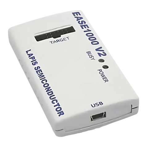
Rohm Lapis EASE1000 V2 User manual

Rohm

Rohm Lapis EASE1000 V2 User manual

Rohm LAPIS Technology RB-D610Q339TB64 User manual

Rohm

Rohm LAPIS Technology RB-D610Q339TB64 User manual

Rohm LAPIS Semiconductor ML620Q151B User manual

Rohm

Rohm LAPIS Semiconductor ML620Q151B User manual

Popular Microcontroller manuals by other brands

Atmel AVR ATtiny15L manual

Atmel

Atmel AVR ATtiny15L manual

ST FP-SNS-SMARTAG1 quick start guide

ST

ST FP-SNS-SMARTAG1 quick start guide

Silicon Laboratories C8051T60x-DK user guide

Silicon Laboratories

Silicon Laboratories C8051T60x-DK user guide

Intrinsyc Open-Q 626 mSOM quick start guide

Intrinsyc

Intrinsyc Open-Q 626 mSOM quick start guide

Stollmann BlueMod+C11/G2 Series Hardware reference

Stollmann

Stollmann BlueMod+C11/G2 Series Hardware reference

NXP Semiconductors LPC29 Series user manual

NXP Semiconductors

NXP Semiconductors LPC29 Series user manual

PLX Technology PEX 8509RDK Hardware reference manual

PLX Technology

PLX Technology PEX 8509RDK Hardware reference manual

Texas Instruments MSP430F6749 manual

Texas Instruments

Texas Instruments MSP430F6749 manual

Altera Cyclone V SoC user guide

Altera

Altera Cyclone V SoC user guide

Dialog Semiconductor SmartBond DA14585 user manual

Dialog Semiconductor

Dialog Semiconductor SmartBond DA14585 user manual

Scon SB017 quick start guide

Scon

Scon SB017 quick start guide

Intel Agilex Configuration user guide

Intel

Intel Agilex Configuration user guide

Renesas RX200 Series user manual

Renesas

Renesas RX200 Series user manual

Renesas RX65N Series Getting started guide

Renesas

Renesas RX65N Series Getting started guide

Seiko Epson S5U1C17W23T manual

Seiko Epson

Seiko Epson S5U1C17W23T manual

mikroElektronika MINI-M4 manual

mikroElektronika

mikroElektronika MINI-M4 manual

Infineon XC800 Series manual

Infineon

Infineon XC800 Series manual

NXP Semiconductors freescale K30 Series Reference manual

NXP Semiconductors

NXP Semiconductors freescale K30 Series Reference manual

manuals.online logo
manuals.online logoBrands
  • About & Mission
  • Contact us
  • Privacy Policy
  • Terms and Conditions

Copyright 2025 Manuals.Online. All Rights Reserved.