Microsemi SA.45s User manual

User Guide
SA.45s Chip-Scale Atomic Clock

SA.45s Chip-Scale Atomic Clock
SA.45s CSAC User Guide Revision D
Contents
1 Revision History ............................................................................................................................. 1
1.1 Revision D ........................................................................................................................................... 1
1.2 Revision C ........................................................................................................................................... 1
1.3 Revision B ........................................................................................................................................... 1
1.4 Revision A ........................................................................................................................................... 1
2 Preface ........................................................................................................................................... 2
2.1 About This Document ......................................................................................................................... 2
2.2 Intended Audience ............................................................................................................................. 2
2.3 Warnings, Cautions, Recommendations, and Notes .......................................................................... 2
2.4 Reference Documents ........................................................................................................................ 2
3 SA.45s Chip-Scale Atomic Clock ..................................................................................................... 3
3.1 Introduction ........................................................................................................................................ 3
3.2 SA.45s Overview ................................................................................................................................. 3
3.2.1 Precautions .............................................................................................................................................. 3
3.2.2 Packaging ................................................................................................................................................. 4
3.2.3 Absolute Minimum and Maximum Ratings ............................................................................................. 4
3.2.4 Mechanical Interface and Mounting Considerations .............................................................................. 4
3.2.5 Recommended Operating Characteristics ............................................................................................... 5
3.3 Functional Description ........................................................................................................................ 6
3.3.1 Principle of Operation ............................................................................................................................. 6
3.3.2 Start-Up Sequence .................................................................................................................................. 7
3.3.3 Built-In Test Equipment (BITE) ................................................................................................................ 7
3.3.4 RF Output Characteristics ........................................................................................................................ 7
3.3.5 What to Expect During First Power-Up ................................................................................................... 8
3.3.6 Frequency Steering .................................................................................................................................. 8
3.3.7 1PPS Output .......................................................................................................................................... 10
3.3.8 1PPS Synchronization ............................................................................................................................ 10
3.3.9 1PPS Disciplining ................................................................................................................................... 12
3.3.10 Time-of-Day ......................................................................................................................................... 13
3.3.11 Analog Tuning ...................................................................................................................................... 14
3.3.12 Ultra-Low Power Operating Mode ...................................................................................................... 15
3.3.13 1PPS Phase Measurement Mode ........................................................................................................ 17
3.4 Programmers Reference ................................................................................................................... 17
3.4.1 Overview of Telemetry Interface .......................................................................................................... 17
3.4.2 Command Summary .............................................................................................................................. 19
3.4.3 Detailed Command Descriptions ........................................................................................................... 20
3.5 Developer's Kit .................................................................................................................................. 29

SA.45s Chip-Scale Atomic Clock
SA.45s CSAC User Guide Revision D
3.5.1 Package Contents .................................................................................................................................. 29
3.5.2 Evaluation Board Overview ................................................................................................................... 29
3.5.3 Installing the CSAC on the Test Fixture ................................................................................................. 31
3.5.4 Cabling ................................................................................................................................................... 31
3.5.5 CSACdemo Software Installation ........................................................................................................... 31
3.5.6 CSACdemo Operation ............................................................................................................................ 31
3.6 Data Acquisition with CSACdemo ..................................................................................................... 34
3.7 Design Guide ..................................................................................................................................... 35
3.7.1 The Art of Disciplining ........................................................................................................................... 35
3.7.2 Heat Sink ............................................................................................................................................... 37
3.7.3 Notes on Soldering ................................................................................................................................ 37
3.7.4 Notes on the Evaluation Board ............................................................................................................. 37
3.7.5 Time Error of a CSAC ............................................................................................................................. 38
3.7.6 Writes to NVRAM .................................................................................................................................. 39

SA.45s Chip-Scale Atomic Clock
SA.45s CSAC User Guide Revision D 1
1 Revision History
The revision history describes the changes that were implemented in the document. The changes are
listed by revision, starting with the most current publication.
1.1 Revision D
Revision D was published in August 2017. It was updated to clarify frequency steering and other edits
per EC12643.
1.2 Revision C
Revision C was published in July 2016. It was updated to reflect 1.08 and 1.09 firmware implementation
as per EC11049.
1.3 Revision B
Revision B was published May 2014. It was updated to reflect 1.06 and 1.07 firmware implementation
and Microsemi branding as per EC09876.
1.4 Revision A
Revision A was published in July 2011. It was the first publication of this document.

SA.45s Chip-Scale Atomic Clock
SA.45s CSAC User Guide Revision D 2
2 Preface
2.1 About This Document
The SA.45s user guide provides basic recommendations for designing products to use Microsemi's
SA.45s Chip-Scale Atomic Clock (CSAC). The guidelines in the document are generic because specific
product requirements vary from one application to the other.
This material consists of a brief description of SA.45s design supported by block diagrams, description of
environmental issues, installation guidelines, and unit operation.
2.2 Intended Audience
This document is intended for engineers and telecommunications professionals who are designing,
installing, operating, or maintaining time, frequency, and synchronization systems having a requirement
for a low profile and highly precise frequency generator.
To use this document effectively, you should have a good understanding of digital telecommunications
technologies and analog frequency generation and synthesis techniques.
2.3 Warnings, Cautions, Recommendations, and Notes
Warning: To avoid serious personal injury or death, do not disregard warnings. All warnings use this
symbol. Warnings are installation, operation, or maintenance procedures, practices, or statements, that
if not strictly observed, may result in serious personal injury or even death.
Caution: To avoid personal injury, do not disregard cautions. All cautions use this symbol. Cautions are
installation, operation, or maintenance procedures, practices, conditions, or statements, that if not
strictly observed, may result in damage to, or destruction of, the equipment. Cautions are also used to
indicate a long-term health hazard.
ESD Caution: To avoid personal injury and electrostatic discharge (ESD) damage to equipment, do not
disregard ESD cautions. All ESD cautions use this symbol. ESD cautions are installation, operation, or
maintenance procedures, practices, conditions, or statements that if not strictly observed, may result in
possible personal injury, electrostatic discharge damage to, or destruction of, static-sensitive
components of the equipment.
Note: All notes use this symbol. Notes contain installation, operation, or maintenance procedures,
practices, conditions, or statements that alert you to important information, which may make your task
easier or increase your understanding.
Note: Microsemi offers training courses designed to enhance your knowledge of the SA.45s Cesium
Frequency Standard. Contact your local representative or sales office for a complete list of courses and
outlines.
2.4 Reference Documents
For additional information about the products described in this guide, please contact your Microsemi
representative or your local sales office. You can also contact us on the web at .www.microsemi.com
CSAC Developer's Kit (990-00123-000)
CSACdemo Software (084-00365-000)
SA.45s Chip-Scale Atomic Clock
SA.45s CSAC User Guide Revision D 3
3 SA.45s Chip-Scale Atomic Clock
3.1 Introduction
The Microsemi Quantum™ Model SA.45s Chip-Scale Atomic Clock (CSAC) is the world's smallest, lowest
power atomic clock technology. This user's reference guide provides the basic guidelines and
recommendations for designing products with the SA.45s reference. These are generic, and should be
tailored for each application.
This document is intended for engineers, technicians, and technologists who are designing, installing,
operating or maintaining time, frequency, and synchronization systems. The SA.45s is a low profile,
highly precise frequency generator. To use this document effectively, an understanding of digital
communication technologies is required. It is advantageous to have a background in frequency
generation and synthesis techniques.
3.2 SA.45s Overview
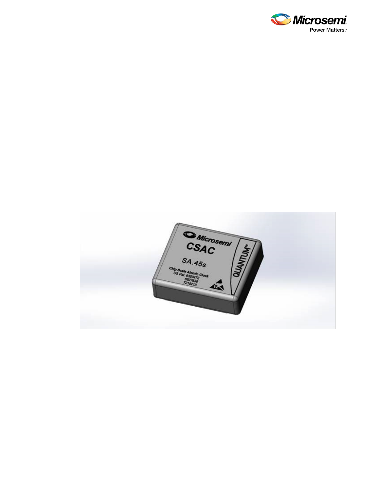
The Microsemi SA.45s CSAC is the world's first commercially available chip-scale atomic clock, providing
the accuracy and stability of atomic clock technology while achieving true breakthroughs in reduced
size, weight, and power consumption. The small size (less than 17 cc) and low power consumption of the
CSAC (less than 125 mW) enables atomic timing accuracy in portable, battery-powered applications.
Figure 1 • Microsemi Quantum SA.45s Chip-Scale Atomic Clock (CSAC)
The SA.45s provides RF and 1PPS outputs at standard CMOS levels. It accepts a 1PPS input to
synchronize the output to within 100 ns of a reference clock. It can also discipline its phase and
frequency to within 1 ns and 1 × 10 , respectively.
–12
This user guide provides engineering information for use of the SA.45s. It also provides supporting
information for use of the developer's kit (p/n 990-00123-00x). Furthermore, the design details of the
developer's kit can be used to assist with host system design (for example, power conditioning or signal
buffering). This guide must be used in conjunction with the current datasheet for SA.45s, which is
available on the Microsemi web site at www.microsemi.com.
3.2.1 Precautions
ESD Caution: To avoid electrostatic discharge (ESD) damage, proper ESD handling procedures must be
observed in unpacking, assembling, and testing the CSAC.
SA.45s Chip-Scale Atomic Clock
SA.45s CSAC User Guide Revision D 4
3.2.2 Packaging
Retain the original CSAC ESD-safe packaging material in the event that the device needs to be returned
to Microsemi for service.
3.2.3 Absolute Minimum and Maximum Ratings
The following table indicates the absolute minimum and maximum ratings to which the CSAC can be
subjected without permanent unrecoverable damage.
The CSAC cannot be expected to perform normally when operated outside of the recommended Note:
operating conditions. All ratings apply at 25°C, unless otherwise noted.
Table 1 • Absolute Maximum Ratings
Parameter Rating
Supply voltage (V )CC 0 V–4.1 V
Analog tuning voltage 0 V–VCC
Maximum current draw 1PPS input, RS232, BITE: ±2 mA
1PPS output, RF output: ±20 mA
Storage temperature –55 °C to 85 °C
Refer to the Note: SA.45s datasheet for updated parameters.
3.2.4 Mechanical Interface and Mounting Considerations
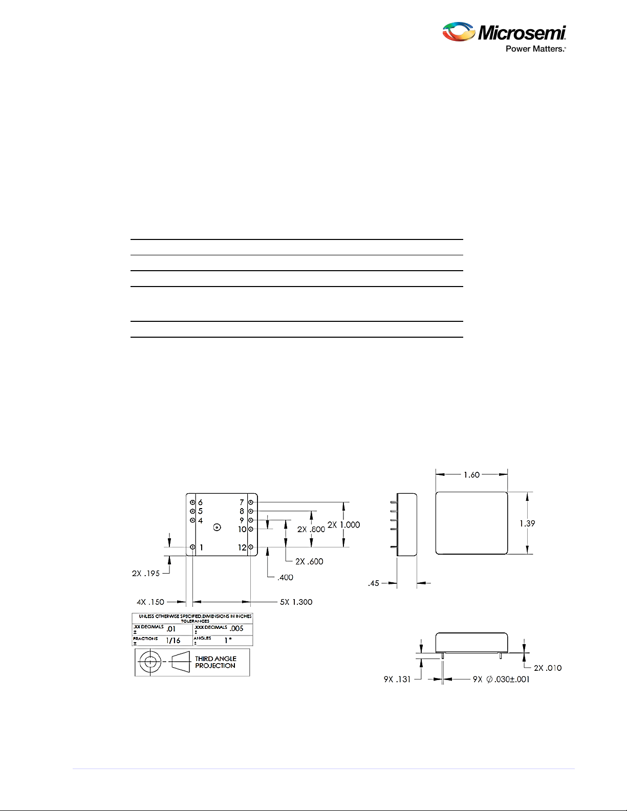
The physical dimensions of the SA.45s CSAC are 1.6" x 1.4" x 0.45" H. The following illustration shows
the detailed dimensions of CSAC. The CSAC baseplate and cover are 80% nickel-iron magnetic alloy per
ASTM A753, Type 4 (Mu-Metal or Hy-Mu80™).
Figure 2 • CSAC Mechanical Drawing
following table The shows the pinout of the SA.45s CSAC.

SA.45s Chip-Scale Atomic Clock
SA.45s CSAC User Guide Revision D 5
Table 2 • SA45s CSAC Pinout
PIN I.D.
1 Tune
Bottom view
2 N/A
3 N/A
4 BITE
5 Tx
6 Rx
7 VCC
8 GND
9 1PPS input
10 1PPS output
11 N/A
12 RF output
Note: Pins labeled N/A are not present in the SA.45s.
3.2.5 Recommended Operating Characteristics
The SA.45 pinout is shown in the previous table . The electrical function of each pin is shown in the
following table.
Table 3 • Recommended Operating Characteristics
PIN Function Level Reference Section
1 Analog tuning input10 V–2.5 V "Analog Tuning" section (see page
14)
4 Built-in test
equipment (BITE)2
LogicH > 2.8 V
LogicL < 0.3 V
"Built-In Test Equipment (BITE)"
section (see page 7)
5, 6 RS232 2.8 V < LogicH < VCC
0 V < LogicL < 0.3 V
"Programmers Reference" section
(see page 17)
7 VCC 3.3 VDC ± 0.1 VDC
8 Ground
9 1PPS in32.5 V < LogicH < VCC
0 V < LogicL < 0.5 V
10 1PPS out4, 5 2.8 V < LogicH < VCC
0 V < LogicL < 0.3 V
"1PPS Output" section (see page
10)
12 RF out 2.8 V < LogicH < VCC
0 V < LogicL < 0.3 V
"RF Output Characteristics" section
(see page 7)
SA.45s Chip-Scale Atomic Clock
SA.45s CSAC User Guide Revision D 6
1.
2.
3.
4.
5.
6.
1.
Notes:
Analog Tuning Sensitivity is Δf/f = (V – 1250 mV) × 1.77 × 10 /mVtune –11
Built-in Test Equipment:
0 = Normal Operation
1 = Unlock Condition
Timing reference is rising edge of input pulse on pin 9.
Output 1PPS is 100 µs in duration for option 001. Refer to the datasheet for other options. (400 µs
for firmware versions 1.06 and earlier).
Timing reference is the rising edge of pin 10. Rise time <10 ns at a load capacitance of 10 pF.
See the for updated parameters.SA.45s datasheet
3.3 Functional Description
The following is a functional description of the CSAC.
3.3.1 Principle of Operation
The CSAC is a passive atomic clock, incorporating the interrogation technique of coherent population
trapping (CPT) and operating on the D1 optical resonance of atomic cesium. A complete description of
passive atomic clocks, CPT, and the CSAC architecture is beyond the scope of this user guide. The
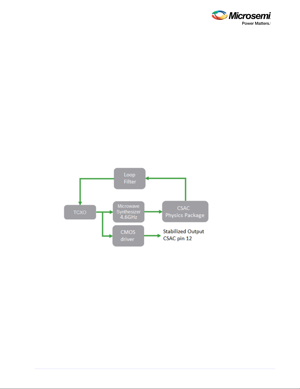
following illustration shows a simplified block diagram of the CSAC.
Figure 3 • Simplified CSAC Block Diagram
The principal RF output from the CSAC is provided by a temperature-compensated crystal oscillator
(TCXO), which is buffered by a CMOS logic gate and provided on the CSAC output pin 12. In normal
operation, the frequency of the TCXO is continuously compared and corrected to ground state hyperfine
frequency of the cesium atoms, contained in the physics package, which thereby improves the stability
and environmental sensitivity of the TCXO by 4–5 orders of magnitude. In addition to the TCXO and the
physics package , the essential components of the CSAC are the microwave synthesizer and the
1
microprocessor . The microwave synthesizer generates 4596.3x MHz with microprocessor-controlled
2
tuning resolution of approximately 1 × 10 . The microprocessor serves multiple functions, including
–12
implementation of the frequency-lock loop filter for the TCXO, optimization of physics package
operation, state-of-health monitoring, and command and control through RS232.
When the CSAC is initially powered on, it performs an acquisition sequence, which includes stabilizing
the temperature of the physics package, optimizing physics package operating parameters, and
acquiring frequency lock to the atomic resonance. The acquisition process may be monitored through
the field of the telemetry (see ). On power-up, the status status "Telemetry (6 and ^)" (see page 20)
begins at 8 (oven warm-up). The status value decrements numerically through the acquisition until
normal operation (status = 0) is achieved.
R. Lutwak, et. al., The Chip-Scale Atomic Clock - Low-Power Physics Package, Proceedings of the 36th
SA.45s Chip-Scale Atomic Clock
SA.45s CSAC User Guide Revision D 7
1.
2.
R. Lutwak, et. al., The Chip-Scale Atomic Clock - Low-Power Physics Package, Proceedings of the 36th
Annual Precise Time and Time Interval (PTTI) Systems and Applications Meeting, December 7–9,
2004, Washington, DC.
R. Lutwak, et. al., The MAC - A Miniature Atomic Clock, Proceedings of the 2005 Joint IEEE
International Frequency Control Symposium and Precise Time & Time Interval Systems &
Applications Meeting, August 29–31, 2005, Vancouver, BC.
3.3.2 Start-Up Sequence
Caution: To avoid severe damage to the unit, do not apply power to the incorrect terminals. The SA.45s
does not have reverse voltage protection.
When power is connected to pin 7, the SA.45s unit begins its warm-up cycle. A signal appears at the
output once power is applied to the unit. This output signal is not stable until the oscillator is locked
(indicated by the BITE pin at CMOS_low).
After 3 minutes, the CSAC achieves Lock and BITE = 0 ( ). "Built-In Test Equipment (BITE)" (see page 7)
Power consumption during warm-up is greater than during normal operation; it is specified on the CSAC
.datasheet
It is recommended to always allow CSAC to remain powered on for >102 seconds after it acquires LOCK.
102 seconds is the minimum amount of time necessary to save CSAC set points to memory. Otherwise,
upon the next power up, the unit may go in to a mode of operation where it re-acquires all of its set
points; warm-up time will then be out of specification.
3.3.3 Built-In Test Equipment (BITE)
CSAC state-of-health can be monitored electronically on pin 4 (BITE) of the SA.45s CSAC. Frequency lock
is indicated both by status = 0 in the status field of telemetry and by the electrical state of the BITE
output pin, which is high (logic 1) upon initial power-on and whenever status ≠ 0. The BITE pin is a high-
impedance CMOS logic output.
Note: When not locked, BITE = 1 and also status ≠ 0 in the status field of the telemetry output string.
At the conclusion of the acquisition sequence (status = 0), BITE remains high for an additional 5 seconds
in order to avoid false indication in the event of acquisition failure. Subsequently, BITE provides an
immediate (within 1 second) indication of lock failure or alarm.
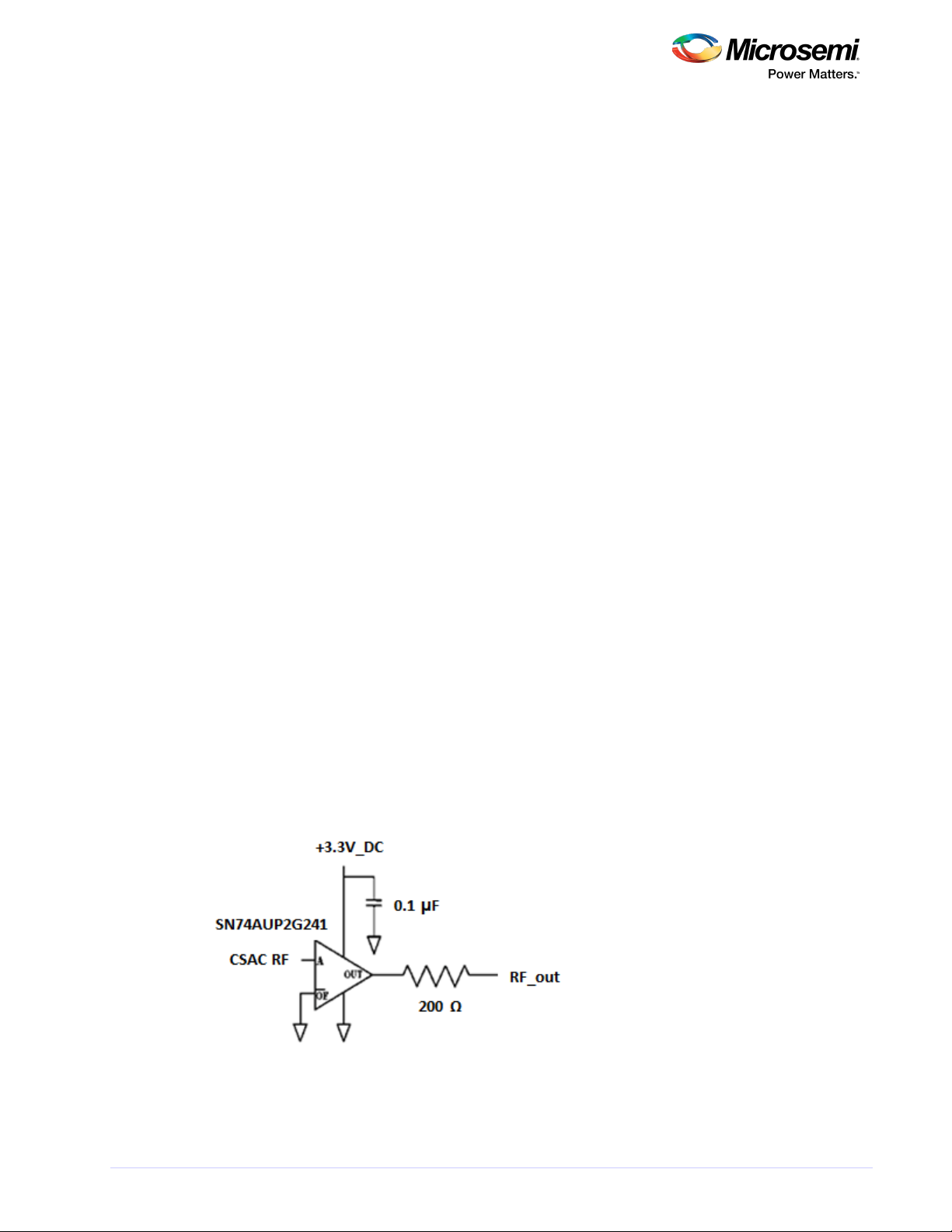
3.3.4 RF Output Characteristics
The buffered CMOS RF output is provided on pin 12 of the SA.45s CSAC. The output series impedance is
200 Ω. For reference, the output driver circuit of the SA.45s is shown in the following illustration.
Figure 4 • CSAC RF Output Driver Circuit
The SA.45s is designed for embedded low-power applications—it is expected to drive a high impedance
input, not a 50 Ω measurement instrument or transmission line.
Note: Driving a 50 Ω line at 13 dBm consumes nearly as much power as the CSAC itself. If a high-level
Table of contents
Popular Clock manuals by other brands

Silicon Laboratories
Silicon Laboratories SI5324 manual

Heathkit
Heathkit GC-1005 Assembly manual

Oregon Scientific
Oregon Scientific PRYSMA RMR221P manual

Andrew O'Malley
Andrew O'Malley DOTKLOK Assembly instructions

ALGE-Timing
ALGE-Timing ASC3 manual

Bodet
Bodet Profil 960 Installation and operating instructions


Progetti
Progetti KALIMERO Directions

La Crosse Technology
La Crosse Technology WT-3141b Quick setup instructions

La Crosse Technology
La Crosse Technology W86531 owner's manual

Sharp
Sharp SPC900 instruction manual

La Crosse Technology
La Crosse Technology 404-50447 quick start guide

Datexx
Datexx DF0063 quick guide