Moog Moogerfooger MF-105M MIDI MuRF User manual

MIDI MuRF Analog Board 11-487
Theory of Operation,
Note: this circuit description refers to the REV A schematic dated 05/19/09.
SHEET 1
EFFECT_IN is the audio signal taken after the bypass switch on page 6. The input network
C5/58-R5-R6-C4 provides DC isolation, radio frequency filtering, and protection of input
amplifier U3A. The output of U3A is the signal AUDIO, which is the amplified audio input
signal.
Negative feedback around U3A goes through U2-A. U2 is a VCA whose gain is controlled by
the current through Q1, which is the sum of the current through R11 and D17/R121. U3B is a
sample-and-hold buffer with level and offset adjustment. The output of this amp determines the
voltage across Rl1.
U14B and associated components are used to buffer, isolate, and attenuate the audio signal from
the audio bus. It is then fed to the MPU to be used as a 0-2.4V DC reference signal for the
compandor circuit. D3 conducts when the peak voltage at U13A is higher than the
COMPANDOR voltage. The COMPANDOR voltage is held by C30 and a capacitor on the
digital board, where it is scanned by the microprocessor. The purpose of the COMPANDOR
voltage is to determine what the highest peak voltage is at the input to the filters. This enables
the microprocessor to determine the status of the overload LED, and perhaps cut down the gain
of the input amplifier to reduce overload distortion.
UI2B is a sample-and-hold buffer with level shifting and gain. Its output is the Direct VCA
CONTROL signal. It controls the overall gain of the direct (non filtered audio) VCA (Sheet 6).
U14A is a sample-and-hold buffer-level shifter / amplifier. Its output is the Filter VCA control
signal. It controls the overall gain of all filter VCAs (Sheets 2 though 5). Note that the Filter
VCA signal is a diode drop across Q16. The current through Q16 is determined by the voltage
at the output of Ul4A and by R50. This is a current mirror configuration. There is a transistor in
each of the filter VCA circuits that matches the properties of Q16.
U10 is a de-multiplexer that routes one of the microprocessor D-A outputs to the inputs of U3B,
U12B, UI4A, and U14B. The signals Mux_A and Mux_B signals select the output routing,
while the signal Mux_EN inhibits U10 when it is high.

SHEET 2
U5B is a comparator and level shifter that takes the signal from the MPU and converts it from
0-3.3V to +/-5V with some hysteresis. This signal is used by the Mux switches to select the
regular or base voicing of the filters.
U5A works in the same way as U5 to convert a duty cycle modulated PWM signal from the
MPU to be used as the shift input to the SHIFT Mux. The duty cycle of this PWM affects the
actual frequency center of the filters. R145/R131/R176 are used to limit the +/-5V swing
slightly to avoid some distortion artifacts in the CD4016.
SHEETS 2 - 5
Sheets 2 through 5 show all eight filters with their respective filter VCAs. With the exception of
the first filter, the circuits are identical topology. Only the two capacitors and two resistors that
set the frequency for each bank change for voice. We will first describe Filters 2 through 8 as
they are all the same and then discuss the difference with filter 1.
Each filter has two modes of primary operation. Those are called Mid Frequency mode and
Base Frequency mode. Normal operation is in Base mode. Mid Frequency Mode is
accomplished by three 4016 switches that switch three parallel resistors around the circuit to
slightly skew the resonant frequency by slightly less than one octave.
First describing base frequency mode: Filter two’s AUDIO signal is applied to the filter
through R55. The filter is a first order band pass filter which consists of U13B, C33, C32, R54
and R66. The output of the filter is at U13B-7.
U23C and U23B switch on and off in response to the SHIFT waveform. When these switches
are on, the filter resonant frequency is raised by about 30%, because R65 and R67 are placed in
parallel with R66 and R54 respectively. When the switches are off, the filter resonant frequency
is not raised. As the duty cycle of the SHIFT signal increases from about 20% to 80%, the
resonant frequency increases about 10%.
To switch from the base voicing to mid frequency voicing the MID_voicing logic signal from
U5B is applied to 2 4016 gates. These gates close two parallel resistors, in this case R146 and
R168 around the filter resistors to change the frequency about an octave.
All filters act as described above with the exception of filter 1. Filter 1, when switched to base
voicing, bypasses the band pass filter and swaps it out with a 2nd order low pass filter. U15C
and U15B swap these out.
Filter 1 uses a DG445 rather than a CD4016 so that it can run from the 9V rails and, hence give
more headroom and less distortion. D116/R136 is used to convert the selector signal to
+5/GND fom +/-5V for U15 and R152/Q51/R150 invert this signal for the base voicing.

The output of the filter is applied through C28 and R41 to the bases of Q10 and Q6. The
transconductance of this transistor pair is proportional to the current through them, which is the
same as the current through Q9.
The network of U11B, R40, and Q5 is a voltage-to-current converter. The input VCA_2 from
the digital board is the envelope voltage for Filter 2. It goes from 0V to +2.4 volts. The voltage
at U11B-7 is such that the current through Q5 in milliamperes is numerically equally to the
voltage at the input to the op amp. Note that U11 has voltage rails of +9 but only -5. This is to
limit the off condition of the output to not swing below -5V and reverse bias Q11.
The current through Q9 is a fraction of the current through Q5. This fraction is determined by
the voltage across R34. If the voltage across R34 is zero, then the current through Q9 is equal to
the voltage across Q5. This is very nearly the case when Q12 is shut off. However, when Q12
conducts, there is a voltage drop across R34, and the current through Q9 is reduced to a fraction
of the current through Q5. This fraction depends only on FILT_VCA_CV, which, in turn,
depends on the voltage at the output of Ul4A (Sheet 1). This is how a single voltage at the
output of Ul4A determines the overall gains of all filter VCAs, regardless of the status of the
envelopes.
The collectors of Q10 and Q6 form a balanced differential pair that is bussed to the
corresponding outputs of the other even filter numbers. This buss then goes to the summing
inputs of the "EVEN” or “RIGHT” output amplifier (Sheet 6). Similarly, the collector outputs
of the off filters (FILT 1, FILT 3, FILT 5, and FILT 7) are bussed and go to the summing inputs
of the "ODD" or “LEFT” amplifier.
SHEET 6
The DIRECT VCA is shown in the upper left corner of the sheet. It is actually two VCAs. One
VCA is for the "RIGHT" side summing amplifier, while the other VCA is for the "LEFT" side
summing amplifier. Thus, the direct signal is fed equally to both audio outputs. The amount that
is fed is determined by the DIRECT_VCA-CV signal (U12B sheet 1), which is derived from the
settings of the MIX and the OUTPUT panel controls on the digital board. Note that the Direct
VCA is fed out of phase to the summing amps from the filter VCAs. This is to compensate for
the phase inversion of the filter amplifiers when adding direct signal back in.
U8A and U8B are the two output amplifiers. They are classic 4 resistor balanced differential
amplifiers with the two input resistors being the impedance of the transistor pairs. Q2 supplies a
smoothed bias voltage of about +7 volts that enables the collectors of the filter VCA's to be
connected directly to the inputs of U8A and U8B.
U6 performs the bypass/on switching functions. The switch signal BYPASS comes from the
digital board. This bypass switch diverts the AUDIO_IN from the jack board either to the Page
1 input filter or directly out as well as switching the output signal from the U8 op amps to the
input signal. The audio feeds to the LEFT/MONO OUT and RIGHT OUT jacks on the jack
board. They are summed to mono on the jack board. Note that when the MFI05 is in bypass,
the bypass output appears only at the LEFT/MONO jack unless JMP11 solder blob is shorted.

SHEET 7
The power inverter and regulators are shown in the upper right corner. D8 provides polarity
protection. It is a low Vf Schottky diode so that the linear regulators do not reach drop out
voltage. D1 conducts if an over voltage situation occurs (power spikes or the wrong input
voltage).
The input +9V is filtered and run to the analog section and the rest of the voltage regulators. U1
produces the +5V analog for the digital and analog PCBs, while U18 produces +5V digital used
on the digital PCB only.
U4 is a 1.4MHz switching regulator of a CuK variety. This provides the -8.25V analog power.
This switcher produces lower ripple output and on the input than a conventional buck/boost.
The switcher should always be operating in the continuous mode of operation (as opposed to
discontinuous operation). If this is not the case then the value of L2 may need to be increased to
provide for continuous operation. L1 provides the switch from Pin 1 of the IC though the cache
diode of D19 and out L2. From there the -9VDC is regulated down to -5VDC via U7 for the
switches and lower noise circuitry of the MuRF.
The negative signal has been reduced from -9V to -8.25V to reduce power loss and to add some
slight asymmetrical clipping to the filter outputs for the characteristic MuRF warm distortion
sound.
The rest of the page consists of two headers. J1 receives all signals from the digital board and
either uses them (mostly on Page 1) or sends them to the jack board via P6.
End of Theory of Operation documentation.
Supply voltage reference:
+5V ±100mV Digital at +5VD TP4 Test point.
+5V ±100mV Analog at +5V TP3 Test Point
-5V ±100mV Analog at -5V TP6 Test Point.
+8.7V +/- 500mV (Raw Power Source = 300mV less than input voltage) on PCB at +9V TP1
Test Point
-8.25V ±200mV Analog on PCB at -8V TP5 Test Point.

MIDI MuRF Digital Board
Test Procedure and Fixture Documentation
NOTE: This document refers to the Test Fixture used in manufacturing. However, most
of the procedures can be followed using a normal, assembled MF-105M MuRF pedal. If
you have any questions about testing the MIDI MuRF, contact
techsupport@moogmusic.com.
MIDI
MIDI may be tested in several ways.
The easiest way is to use the MIDI testing tab of the Moog utility “MIDI_MuRF.exe”
The first tab has some MIDI controls on it.
Other ways include using a simple sequencer that may be downloaded from
http://www.reaper.fm/download.php
Alternatively MiDI OX
http://www.midiox.com/
may be used or a simple MiDI controller keyboard such as an M-Audio Oxygen 8
http://www.m-audio.com/products/en_us/Oxygen8v2.html

MIDI MuRF DIGITAL BOARD CHECKOUT PROCEDURE
Modified July 2009 from the original May 28, 2004
Version
Initial Firmware load and check out
1. Install B.U.T.
•Place the Digital Board Under Test onto test fixture and clamp down.
a) Verify that there is an insolated washer on each screw terminal before
placing B.U.T on PCB.
b) Add hold down nut to each screw stud. Verify insolated washer is glued to
each hold down nut.
c) Clamp fixture clamp onto J1 making sure that it makes only a slight push
on PCB and that clamp does not hit RN4 or any other part.
•Verify test fixture pogo pins line up with pads on J1.
•Verify LEDs can bend forward 9 degrees from the PCB.
•Connect stomp cable to J3 on B.U.T.
•Connect JTAG programmer to J4 (Red pin 1 stripe to middle of PCB)
•Connect MIDI Out device to test fixture MIDI IN jack
•Apply +9.5V +/- 1V power to the fixture.
2. Turn all controls on BOTH the board under test (B.U.T.) AND the test fixture to the
center position. Set the Pattern Selector switch to position 2. Raise all 8 faders to the top
(full on). Set the tap switch to “off”. If the B.U.T. has not yet been loaded with firmware,
the +9.5V current going in to the test fixture should be around 140mA (+/- 20mA).
3. Load the boot loader firmware onto the MPU using the Silabs USB JTAG programmer
(DK# 336-1182-ND) via J4 on the BUT. The Red Pin 1 side goes to the middle of the
PCB.
•On the Connect/Disconnect tab select JTAG interface, apply power to the BUT and
select “Connect”.
•From the Download tab select the current Boot Loader file (
“MM_Booter_v1.0_122.hex” as of this writing) and check “Erase all code space
before download”.
•Press Download and when complete press Go. The unit will flash an initialization
sequence on the three LEDs.
•When done the three LEDs on the BUT should light up green and input current
should increase slightly to around 175mA (+/- 20mA).
•Press Halt, on the download tab.
•Press Disconnect on the Connect Disconnect Tab
•Power down B.U.T. and remove JTAG programmer.
4. Power B.U.T. back up and verify the following voltages and conditions. (note you may
connect ground to the loop below the MIDI connector).
•All three green LEDs are lit up. (Note if this does not happen due to reworked board
power up with two B.U.T. switches to right while pressing bypass switch to boot in
bootloader mode).
•Verify total 9.5V current draw is under 200mA (around 165mA)
•Verify +3.30V +/- 75mV at TP3.
•Verify +3.27V +100mV / - 75mV at TP4. Verify that this voltage is slightly lower
than the TP3 voltage.
•Verify +2.43V +/- 50mV right leg of any pot. (Note this voltage will not come up
before boot loader is installed)
•Verify +5V +/- 100mV at J1-2 (Note: This voltage is generated on test fixture not
BUT)
•Verify -5V +/-100 mV at J1-1 (Note: This voltage is generated on test fixture not
BUT)

5. Run the Moog “MM_Tester_v1.0_122.exe” application to finish programming.
a. If there are not 3 green LEDS on the B.U.T then boot in hidden mode by sliding
LFO and FREQ switches to the right and powering up with the bypass button
pressed. (note this is required for booter 1.0)
b. Select your MIDI output device, set to Channel 1 and click on “Open MIDI”
c. Select the Firmware tab and hit … to brows for the current MIDI firmware.hex file
(MM_Firmware_v0.5_121.hex.as of this writing). Note please check with Moog
Music for the current firmware before each major MIDI MuRF build as the
firmware is always being updated.
d. Click the Download button and watch the status window on the application as well
as the B.U.T. On the B.U.T. you should see BYPASS LED blinking red and green
as data transfers. Then the DRIVE and RATE LEDs will turn red and the BYPASS
LED blinks very fast as data is verified and copied into memory. If successful, unit
will reboot into normal MIDI MuRF operating mode.
e. Note that the pattern LEDS are flashing in unison. Click on Patterns TAB, select
Factory Defaults, Pattern All, Same and click Download. You should see the
Bypass LED blink read and green as data transfers. When done the patterns LEDs
will not flash in an orderly fashion. If the pattern switch is set to pattern #2 then
they will move from right to left, one LED at a time.
f. Select the Tables tab and click download. You should see the Bypass LED blink
read and green as data transfers.

UI and I/O Testing.
6. ON/BYPASS FUNCTION (“Stomp Switch”): Press the Bypass STOMP SWITCH on the
tester panel.
a. The middle LED on the B.U.T. should alternate between green and red. (Tests LED
and Switch input to MPU)
b. The BYPASS / ON LED on the fixture panel should light up yellow when the LED
on the B.U.T. is green, but turn off when it is red. (Tests Bypass output from MPU)
7. ENVELOPE OUTPUTS: On the fixture panel, set the RATE EXTERNAL, MIX
EXTERNAL, ENVELOPE EXTERNAL, and LFO/SWEEP EXTERNAL knobs to their
mid positions. Set the TAP ENABLE switch up (OFF position). On the B.U.T., place a knob
on the rotary pattern selector, then set the ENVELOPE and RATE controls to their mid
positions (note ENVELOPE slightly to the left of center works best). Set the LFO (was
BANK) switch to the left (OFF) position. Set the VOICING switch to the Mids position
(right). Set the PATTERN selector to position #2, and raise all the sliders. Be sure the
BYPASS light is green (on).
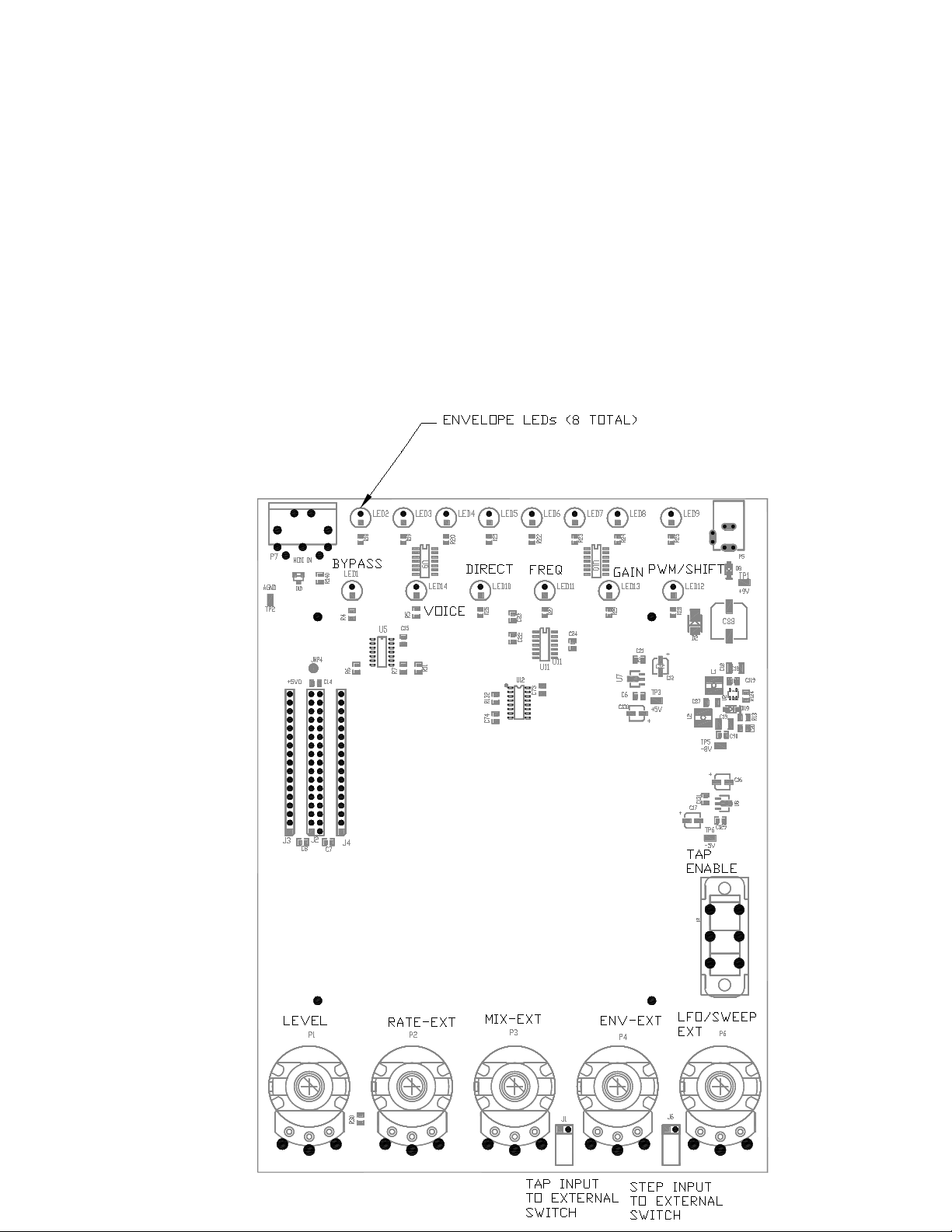
a. The ENVELOPE LEDs should all light up in sequence, one at a time from right to
left.
b. Set the PATTERN selector to position #1. The ENVELOPE LEDs should now all be
on and not moving. Raise and then and lower each slider in turn.
c. The sliders should move smoothly. Each LED should get dim and then bright as its
corresponding slider is moved down and then up.
If you observe these conditions, then the envelope outputs are working (Jl-5 to Jl-12) and
the sliders are mechanically OK.
8. PATTERN RATE: On the B.U.T., set the PATTERN selector back to #2. On the fixture
panel, turn the ENVELOPE EXTERNAL Pot full CCW.
a. Turn the RATE EXTERNAL pot slowly through its entire range.
b. The speed at which the Envelope LEDs sequence should change from very slow to
very fast. They should step at a rate of about two envelopes per second when the
RATE EXTERNAL pot and the RATE pot are both in mid position. Return the
RATE EXTERNAL pot in mid position.
c. Turn the RATE pot slowly through its range and observer that the speed at which the
Envelope LEDs sequence should change from very slow to very fast.
d. Return the RATE pot to the middle position/
If you observe the conditions, then the RATE pot and the RATE EXTERNAL input are
working.
9. ENVELOPE SHAPE: Set the RATE pot in mid-position. On the fixture panel, turn
the ENVELOPE EXTERNAL pot slowly through its entire range.
a. The individual envelope LEDs should indicate that the envelope shape is
changing. The envelopes should be very short when the ENVELOPE
EXTERNAL pot is at either extreme, or long when the pot is in the middle.
b. Now set the ENVELOPE EXTERNAL pot in mid position. On the B.U.T.,

turn the ENVELOPE pot slowly through its range.
c. The individual envelope LEDs should indicate that the envelope shape is changing.
The envelopes should be very short when the ENVELOPE pot is at either extreme, or
long when the pot is in the middle.
If you observe the conditions, then the ENVELOPE pot and the ENVELOPE
EXTERNAL input are working.
10. AUDIO LEVEL INDICATOR: On the fixture panel, turn the AUDIO LEVEL
pot through its entire range.
a. The left-most DRIVE LED on the B.U.T. should go from not illuminated, to
green, to orange, to red, as you turn the AUDIO LEVEL pot counter-
clockwise. It should be orange in the middle position.
If you observe this condition, then the “compandor” voltage input (Jl- 13) and the OVERLOAD
led are working.
11. AUDIO INPUT GAIN: On the B.U.T., turn the DRIVE pot slowly clockwise.
a. The orange GAIN ( INPUT LEVEL) LED on the fixture panel should go from
brightly lit to completely off. No other orange LEDs should change at this time. This
verifies that the the DRIVE pot, CV_DAC output (Jl-14), and the mux bits
(J1.28,29,31) are all working.
12. MIX POT AND PEDAL INPUT: On the B.U.T., set the MIX pot in mid position and
the OUTPUT pot full clockwise. Then turn The MIX EXTERNAL pot slowly
clockwise through its range.
a. Both the Direct VCA and Filter VCA (Formally D-control and the F-control) LEDS
should go from brightly lit to completely off as you do this. If you observe any rapid
or choppy movement it indicates that the mix tables have not been properly loaded
from the MIDI MuRF Application.
Put the MIX EXTERNAL pot in mid position. On the B.U.T., turn the MIX pot slowly
clockwise through its range.
b. The same thing as above should happen: Both the Direct control and the Filter control
LEDs should go from brightly lit to completely off as you do this.
If you observe this condition, then the MIX pot and the MIX pedal input are both working.
13. OUTPUT LEVEL: Set both the MIX pots to mid position. On the B.U.T., slowly turn the
OUTPUT pot clockwise through its entire range.
a. The Direct VCA control LED should get brighter and the Filter VCA control LED
should get dimmer as you do this.
b. Set the MIX KNOB Full Counter Clock Wise (Dry) and note that moving the Output
knob dims the direct LED but the filter LED remains unchanged (full on)
c. Set the MIX KNOB Full Clock Wise (Wet) and note that moving the Output knob
dims the filter LED but the drive LED remains unchanged (full off)
If you observe this condition, then the OUTPUT pot is working.
14. LFO/SWEEP: On the B.U.T., set the bank switch to LFO On (right position). On the fixture
panel, set the LFO/SWEEP EXTERNAL control to mid position.

a. The LFO/PWM RATE LED should pulsate at a rate of a few times a second.
Now slowly vary turn the LFO/SWEEP EXTERNAL control clockwise through its range.
b. The pulsation of the LFO/PWM LED should vary from very slow to very fast.
Flip the LFO switch back to OFF (left)
c. Adjusting the LFO/SWEEP EXTERNAL should now chance brightness of the
LFO/PWM LED but it should remain on.
If you observe these conditions, then the LFO/SWEEP pedal input and the BANK switch are
working.
15. Voicing:On the B.U.T. Set the Voicing switch to the left (Low) position. Verify that the
Voicing LED on the fixture panel toggles and that the patterns change. The LED should be
on in MIDs position and off in BASS position.
16. PATTERN SELECTOR: The object of this step is to ensure that all twelve positions of
the selector switch are properly connected to the microprocessor through the muxing
diodes. This requires that the test technician watch the envelope LED patterns carefully to
ensure that they correspond to the position of the selector switch.
a. On the fixture panel, set the RATE EXTERNAL knob and the ENVELOPE
EXTERNAL knob to mid position. Be sure that the TAP ENABLE toggle switch is
down (off). On the B.U.T., set the RATE knob to mid position. Set the ENVELOPE
knob to 8 or 9 o'clock, so that the pulsations of the envelope LEDs are short enough
to be distinct but long enough to be easily visible.
b. Now, starting with position #1, turn the PATTERN selector through the twelve
positions. After switching to each position, carefully note the sequencing pattern of
the envelope LEDs.
c. You should see the following patterns. See the MIDI MuRF Manual for
representations of these patterns.
If you observe these patterns, then the PATTERN selector switch is working properly.
17. TAP FUNCTION: Note the right hand (RATE) LED on the B.U.T.
a. The RATE LED should be blinking red.
On the fixture panel, turn the TAP ENABLE switch on (down). Then tap the TAP switch three
times at a rate of about once a second.
b. The RATE LED should now be blinking green, at the rate that you tapped.
Tap the switch 3 times fast and verify that the speed increases to that speed.
Now turn the TAP ENABLE Switch off (up.
c. The RATE LED should now be blinking red at the rate that is set by the RATE
controls.
If you observe all three of these conditions, then the RATE LED, the TAP ENABLE input, and
the TAP input are working correctly.
18. Step Function:With the Tap enable still engaged hit the step momentary switch
a. Note the LEDS sequence only once with each step pushbutton hit
19. MIDI Input. Optional test.

MIDI is verified by loading the application firmware. However if the application is already
loaded it may be necessary to use another MIDI verification test. If so run MIDI_MuRF.exe
and connect a midi channel.
Using the control tabs adjust a slider or button and verify that the B.U.T functions as if that
knob was changed on the B.U.T. For example, if changing the RATE slider the RATE LED
speed changes. The RATE LED will change to Orange to indicate it has received MIDI
data.

Appendix A – MIDI CC Messages
The following MIDI Control Change messages are recognized:
CC1 – Envelope (Note – one of the most expressive ways to “play” the MuRF is to modulate the
Envelope time control manually – a mod wheel would be the perfect type of controller for this –
especially if you are using one of the Note On modes) CC Value 000-003 = Env value 1, CC Value 004-
007 = Env value 2, etc… (128 CC values/32 Env Values)
CC2 – Drive – Values 0-127 = changes of 32 12-bit values/ MIDI CC step
CC3 – LFO Rate/Sweep = Values 0-127. Note When LFO is Off – CC3 functions as “Sweep”; When
LFO is On and “free running” CC3 is the LFO Rate, CC Values 0-127 = LFO Rates .08Hz to 25Hz.
When LFO is On and MIDI MuRF is receiving System Realtime Clock Messages, CC3 functions as a
Clock divider with 16 possible settings for the LFO rate (see Clock divider chart below).
CC7 – Output Level (Standard MIDI Volume command) Values 0-127
CC8 – Mix Values 0-127
CC9 – Pattern Clock Rate. Note that w/no MIDI Clock messages being received, this is a continuous
control the same range as the front panel control. When synced to MIDI, this CC becomes a Clock divider
– with 16 possible settings. (See Clock Divider chart below).
CC85 – LFO On/Off. Values: 0=OFF; 127=ON
CC86 – Freq Bass/Mids. Values 0=OFF; 127=ON
CC87 – Bypass On/Off. Values 0=Off; 127=ON
CC88 – LFO Sync On/Off Values 0=Off; 127= ON (should default to ON). Can enable/disable sync LFO
Rate to MIDI Clock
CC89 – Pattern Clock Sync On/Off. Values 0=OFF; 127= ON (should default to ON). Can enable/disable
sync pattern clock to MIDI Clock
CCs 20-27 – Filters 1-8 EGR_CV DAC Level – receiving any of these CC messages stops the pattern
clock and allows Realtime MIDI tweaking of the DAC levels for each Filter EGR signal. Changing the
Panel Rate control, Rate CV input, or receiving a MIDI Clock start or Clock Continue message restarts
Pattern clock and returns EGRs to Pattern function.
CC102 – MIDI Channel – this is the only Channel Voice Message hat the MuRF responds to an ANY
channel – Values 0-15 = MIDI Channels 1-16.

Quick firmware installation guide for MIDI MuRF:
1.) load "bootloader" firmware (MM_Booter_v1.0_122.hex) via Silabs USB Debug Adapter and Silabs Flash
Programming Utility software for Windows-PC. Flash Programming Utility software can be downloaded (as of 11-
2009) from this link:
https://www.silabs.com/Support%20Documents/Software/UtilDLL.zip
2.) Cycle power to unit; all LEDs should be green. If not, boot to "hidden mode" by sliding LFO and FREQ
switches to the right and powering up with the bypass button pressed.
3.) Connect MIDI output from your computer to the MuRF MIDI IN. Open the software "MIDI_MuRF V0.94
B134.exe" and on the Device menu, select your MIDI output device. Click Open MIDI.
4.) Select the Firmware tab and hit [...] to browse for the current MIDI firmware.hex file
(MIDIMurf_firmware_v1_4_142.hex as of this writing).
5.) Click the Download button and watch the status window on the application as well as the B.U.T. On the B.U.T.
you should see BYPASS LED blinking red and green as data transfers. Then the DRIVE and RATE LEDs will turn
red and the BYPASS LED blinks very fast as data is verified and copied into memory. If successful, unit will reboot
into normal MIDI MuRF operating mode.
6.) Select the Patterns tab in the MIDI MuRF software; defaults should be Pattern: ALL, Download As: SAME.
Click Download.
7.) Select the Tables tab and click Download.
MIDI MuRF should now be running current firmware with all patterns and tables loaded with factory default data.
Table of contents
Other Moog Recording Equipment manuals


Popular Recording Equipment manuals by other brands


Leightronix
Leightronix LabVault-SD Installation, configuration, and operation manual

Fostex
Fostex G16S owner's manual

Unico
Unico DUAL PLUS 1C Manual of installation and use

DEVA Broadcast
DEVA Broadcast DB910 Quick user guide

YASKAWA
YASKAWA 46S03153-0010 manual

Cabletron Systems
Cabletron Systems DELHF-UA user guide