MSC 8009 User manual

USER'S
MANUAL
FOR
MSC
8C)09
Infcrmaticn
contained
in
this
manual
is
disclosed
in
confidence
and
may
not
be
duplicated
in
full
or
in
part
by
any
person without priolr
written
approval
of
Mcneli
thic
Systems
Corporation.
Its
sole
purpcse
is
to
provide
the
user
with
adequately
detailed
documentation so
as
to
efficiently
install,
operate',
maintain,
and
order
spare
parts
for
the
system
supplied.
The
use
of
this
doc~~ent
for
all
other
purpcses
is
specifically
prohibited.
C:OPYRIGHT
©
1980
BY
MONOLITHIC
SYSTEMS
CORPORATION
84
In~erness
Circle
East
Englewood, Colorado, 80112
(303) 170-7400
PRELIMINARY
2-26-81
~-------------------------,---------
,---------------------------------,--~

1. 1
1. 2
1. 3
1. 4
1. 5
1. 6
1. 7
1. 8
1. 9
1.10
1.
11
1.
12
1.
13
1•
14
SCOPE
SPECIFICATIONS
FUNCTIONAL
DESCRIPTION
Z80A
PROCESSOR
MSC
8009
TABLE
OF
CONTENTS
SECTION
1
INTRODUCTION
ARITHMETIC
PROCESSING
UNIT
(Optional)
1. 5. 1
9511
APU
1. 5. 2
9512
APU
BUS
INTERFACE
MODE
STATUS
REGISTER
1.
7.
1
Bus
Exchange
Modes
READ/WRITE
MEMORY
1. 8. 1 Refresh Cycle
READ
ONLY
MEMORY
1. 9. 1
Protection
PROM
DUAL
MAP
CONFIGURATION
(Optional)
I/O
INTERFACE
1.11. 1
Serial
I/O
Interfaces
FLOPPY
DISK
INTERFACE
1.12.
1 Disk Format
~.12.
2
Status
Register
1.12. 2. 1 Address
Marks
1.12.
2. 2 Cyclic Redundancy
Check
Characters
(CRC)
INTERRUPT
1.13.
1 Non-Maskable
Interrupt
SYSTEM
CONTROL
1.14. 1 System
~lock
1.14. 2
Power
Up
1.14. 3
Memory
And
I/O Addressing
1.14. 4
Watchdog
Timer
1-
1
1-
2
1-
7
1-
7
1-
8
1-
8
1-
8
1-
9
1-
9
1-
9
1-10
1-10
1-10
1-10
1-11
1-11
1-11
1-12
1-12
1-12
1-13
1-13
1-13
1-14
1-14
1-14
1-14
1-15
1-15

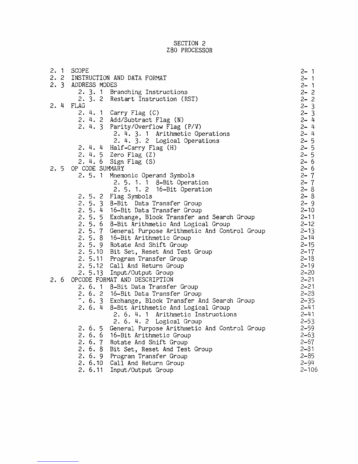
2.
1
2.
2
2.
3
2. 4
2.
5
2.
6
SCOPE
INSTRUCTION
AND
DATA
FORMAT
ADDRESS
MODES
SECTION
2
zao
PROCESSOR
2.
3. 1 Branching
Instructions
2.
3. 2
Restart
Instruction
(RST)
FLAG
2.
4.
1
2.
4.
2
2.
4.
3
Carry
Flag
(C)
Add/Subtr'
act
Flag
(N)
Parity/Overflow
Flag (P/V)
2. 4. 3
..
1 Arithmetic Operations
2.
4. 3
..
2 Logical Operations
2. 4. 4 Half-Carry Flag
(H)
2.
4. 5 Zero Flag
(Z)
2. 4. 6 Sign
Flag
(S)
OP
CODE
SUMMARY
2.
5. 1
Mnemonic
Operand Symbols
2. 5. 1. 1
8-Bit
Operation
2.
5.
1~
2 16-Bit Operation
2.
5. 2 Flag Symbols
2. 5. 3
8-Bit
Data
Transfer
Group
2.
5. 4
16-Bit
Data
Transfer
Group
2.
5. 5 Exchange t Block
Transfer
and Search Group
2.
5.
6
8-Bit
Ari.thmetic
And
Logical Group
2.
5.
7 General Purpose Arithmetic
And
Control Group
2.
5.
8
16-Bit
Arithmetic
Group
2.
5. 9 Rotate
And
Shift
Group
2.
5.10
Bit
Set,
Reset
And
Test
Group
2. 5.11 Program
Transfer
Group
2.
5.12
Call
And
Return
Group
2.
5.13
Input/Output
Group
OPCODE
FORMAT
AND
DESCRIPTION
2.
6. 1
8-Bit
Data
Transfer
Group
2.
6.
2 16--Bit Data
Transfer
Group
,..
6. 3
Exc!hange,
Block
Transfer
And
Search
Group
2. 6. 4
8-Bit
Arithmetic
And
Logical Group
2
..
6. 4. 1
Arithmetic
Instructions
2
..
6.
4.
2 Logical Group
2.
6. 5 General Purpose
Arithmetic
And
Control Group
2.
6. 6
16-Bit
Ar'ithmetic
Group
2.
6. 7 Rotate
And
Shift
Group
2.
6. 8
Bit
Set,
Reset
And
Test
Group
2.
6.
9 Program
Transfer
Group
2.
6.10
Call
And
Return Group
2.
6.11 Input/Output
Group
2-
1
2-
1
2-
1
2-
2
2-
2
2-
3
2-
3
2-
4
2-
4
2-
4
2-
5
2-
5
2-
5
2-
6
2-
6
2-
7
2-
7
2-
8
2-
8
2-
9
2-10
2-11
2-12
2-13
2-14
2-15
2-17
2-18
2-19
2-20
2-21
2-21
2-23
2-35
2-41
2-41
2-53
2-59
2-63
2-67
2-81
2-85
2-94
2-106

3.
1
SCOPE
SECTION
3
MULTI
BUS
3. 2
MULTIBUS
CONVENTION
3. 3
MULTIBUS
CONTROL
3. 3. 1
Bus
Contention Resolution
3..
3.
1.
1
Serial
Bus
Priority
3. 3.
1.
2
Parallel
Bus
Priority
3. 3.
1.
3
Bus
Exchange
Modes
3. 3. 2 Acknowledge
Signals
3.
3.
2. 1
Transfer
Acknowledge
(XACK/)
3..
3.
2.
2 Advance Acknowledge
(AACK/)
3.
4
SPECIFICATIONS
3. 4. 1
Electrical
Characteristics
3. 4. 2 Mechanical
Characteristics
3. 4. 3 Signal
Description
3.
4.
4 Data
Transfer
Timing
3. 5
MSC
8009
CONFIGURATION
Figure
3- 1
Figure
3- 2
Figure
3- 3
Figure
3- 4
Table 3- 1
Table 3- 2
4. 1
SCOPE
SERIAL-BUS
CONTENTION
CONFIGURATION
Z80
READ
OPERATION
Z80
WRITE
OPERATION
MULTI
BUS
DATA
TRANSFER
TIMING
MULTI
BUS
LEVEL
SPECIFICATIONS
MULTI
BUS
ELECTRICAL
REQUIREMENTS
SECTION
4
MEMORY
4. 2
R~~
CONFIGURATION
4. 2. 1 Addressing
4. 2. 2
Memory
Read
4. 2. 3
Memory
Write
4. 2. 4 Refresh Cycle
4. 3
EPROM/R~1
CONFIGU
HATION
4. 3. 1
EPROM/HOM
Addressing
4. 3. 2
Memory
Protect
4. 4
DUAL
MAP
CONFIGURATION
(OPTIONAL)
Table
4-
1
Table
4-
2
PROGRAM
~IEMORY
JUMPER
CONNECTIONS
MEMORY
ALLOCATION
3- 1
3-
1
3- 2
3- 2
3- 3
3-
4
3- 4
3- 5
3- 5
3- 8
3- 8
3- 8
3- 8
3-10
3-11
3-13
3- 3
3- 6
3- 7
3-14
3- 9
3-15
4-
1
4-
1
4-
2
4-
2
4-
2
4-
3
4- 4
4-
4
4-
5
4-
5
4-
3
4-
6

SECTION
5
SERIAL
I/O
INTERFACE
5. 1
SCOPE
5-
1
5. 2
CONFIGURING
THE
SERIAL
I/O
PORT
5-
1
5. 2. 1 Terminal/Communication Configuration
5-
1
5. 2. 2 Programmable
Timer
Configuration
5-
1
5. 2. 2. 1
BAUD
Rate Configuration
5-
5
5. 2. 3 Clock Configurations
5-
5
5. 2. 4
EIA
RS·-232-C
Configuration
5-
6
5. 2. 5
TTL
Conflguration
5-
6
5. 2. 6 Current.
Loop
Operation
5-
1
5. 2. 1
Interrupt
Configuration
5-
1
5. 3
PROGRAMMING
THE
SERIAL
I/O
INTERFACE
5-
9
5. 3. 1
Initialization
5-
9
5. 3. 2 Clock Set
5-
9
5.
3.
3 Control
~lord
Programming
5-
9
5
..
3. 3. 1
Mode
Instruction
5-11
5.
3.
3. 2
Command
Instruction
5-11
5. 3. 4
Status
Word
Format 5-13
5
..
3. 4. 1
Parity
Error 5-13
5. 3. 4. 2 Overrun Error 5-14
5
..
3. 4. 3 Framing Error 5-14
5. 4
DATA
COMMUNICATION
5-14
5. 4. 1
Asynchl"onous
Transmission 5-14
5. 4. 2 Asynchronous Receive 5-14
5.
4. 3 Synchronous Transmission 5-15
5. 4. 4 Synchronous
Rece
i
ve
5-15
5. 5
TIMER
INTERFACE
5-17
5.5.
1
JJJode
Definitions
5-18
5
..
5. 1. 1
HODE
0 -
Interrupt
On
Tenninal Count 5-19
5..
5.
1. 2
MODE
1 - Progralmnable
One
Shot 5-20
5. 5. 1. 3
MODE
2 - Rate Generator 5-21
5. 5. 1. 4
MODE
3 - Square
Wave
Generator 5-22
5.
5.
1. 5
MODE
4 - Software Triggered Strobe 5-23
5. 5. 1. 6
MODE
5 - Hardware Trigger Strobe 5-24
5. 5. 2
On-The--FlY
Readout 5-25
5. 5. 3
BAUD
Rate Generator 5-25
Figure
5-
Figure 5- 2
Figure
5-
3
Figure 5- 4
Figure
5-
5
Figure
5-
6
Figure
5-
1
Figure 5- 8
Figure
5-
9
Figure 5-10
Figure 5-11
Figure 5-12
Figure 5-13
CONTROL
WORD
SEQUENCE
MODE
INSTRUCTION
CONTROL
WORD
FORMAT
COMMAND
INSTRUCTION
CONTROL
WORD
FORMAT
STATUS
WORD
FORMAT
SYNC
CHARACTER
TRANSMISSION
8253
INTERVAL
TIMER
CONTROL
WORD
FORMAT
MODE
0
TIMING
DIAGRAM
MODE
1
TIMING
DIAGRAIJJ
MODE
2
TIMING
DIAGRAM
MODE
3
TIMING
DIAGRAM
MODE
4
TllV1ING
DIAGRAM
MODE
5
TIMING
DIAGRAM
BAUD
RATE
GENERATOR
ROUTINE
5- 8
5-10
5-12
5-13
5-16
5-17
5-19
5-20
5-21
5-22
5-23
5-24
5-26
Table
5-
SERIAL
1/0
CABLE
CONNECTION
FOR
DATA
COM~1UNICATIONS
EQUIPMENT
(DCE)
Table 5- 2
SERIAL
1/0
CABLE
CONNECTION
FOR
DATA
COMMUNICATIONS
EQUIPMENT
(DTE)
Table
5-
3
SERIAL
I/O
PORT
CONFIGURATION
Table
5-
4
PRCXJ
RA]-1MABLE
TIME
R
SIGNALS
Table
5-
5
8253
TIMER
PORT
ADDRESSES
Table
5-
6
8253
TIMER
REGISTER
BAUD
RATE
VALUES
SECTION
6
FLOPPY-DISK
FORMATTER/CONTROLLER
6.
1
SCOPE
6. 2
DESCRIPTION
6. 3
CONTROL
REGISTERS
6. 3. 1
Command
Hegister
6.
3. 1. 1 Unit
Register
6. 3. 1. 2
Command
Register
6.
3.
2
Status
Register
6. 3. 3 Track
Register
6. 3. 4 Sector
Register
6. 3. 5 Data
Register
6. 4
COMHAND
STRUCTURE
6. 4. 1
Head
Positioning
Commands
(Type
1)
6. 4. 2 Sector
Comnands
(Type
2)
6. 4. 3 Track
Commands
(Type
3)
6. 4. 4 Reset
Interrupt
(Type
4)
6. 4. 5 Write Precompensation
6. 5
FORMATTING
THE
DISK
6. 6. 1 Shugart Drives
6.
6.
1. 1
Gaps
6. 6. 1. 2 Address
Marks
6. 6. 1. 3 Cyclic Redundancy
Check
Character
6. 6. 1. 4
Setting
Up
The
Disk
6. 6. 2
IBM
Format
Figure
6-
1
Figure
6-
2
Figure
6- 3
Figure
6-
4
Figure
6- 5
Figure
6-
6
Figure
6- 7
Figure
6- 8
Figure
6- 9
Figure
6-10
6. 6. 2. 1
IBM
3740
(Single
Density)
6. 6. 2. 2
IBM
System
34
(Double Density)
COMMAND
FtOUTINE
STATUS
REGISTER
READ
DISK
SECTOR
FORMAT
TRACK
SEEK
FROM
TRACK
00
TRACK
SEEK
SECTOR
READ
ROUTINE
SECTOR
WRITE
ROUTINE
READ
ADDRESS
ROUTINE
RESET
INTERRUPT
ROUTINE
DISK
INITIALIZATION
ROUTINE
5-
?
<-
5-
3
5-
4
5-
4
5-25
5-25
6-
1
6- 1
6-
1
6-
4
6-
4
6-
4
6-
4
6-
8
6-
8
6- 8
6-
9
6-
9
6-11
6-11,.
6-15
6-15
6-15
6-17
6-18
6-19
(CRC)
6-19
6-19
6-20
6-20
6-21
6-
3
6-
5
6-17
6-22
6-24
6-26
6-28
6-30
6-32
6-33

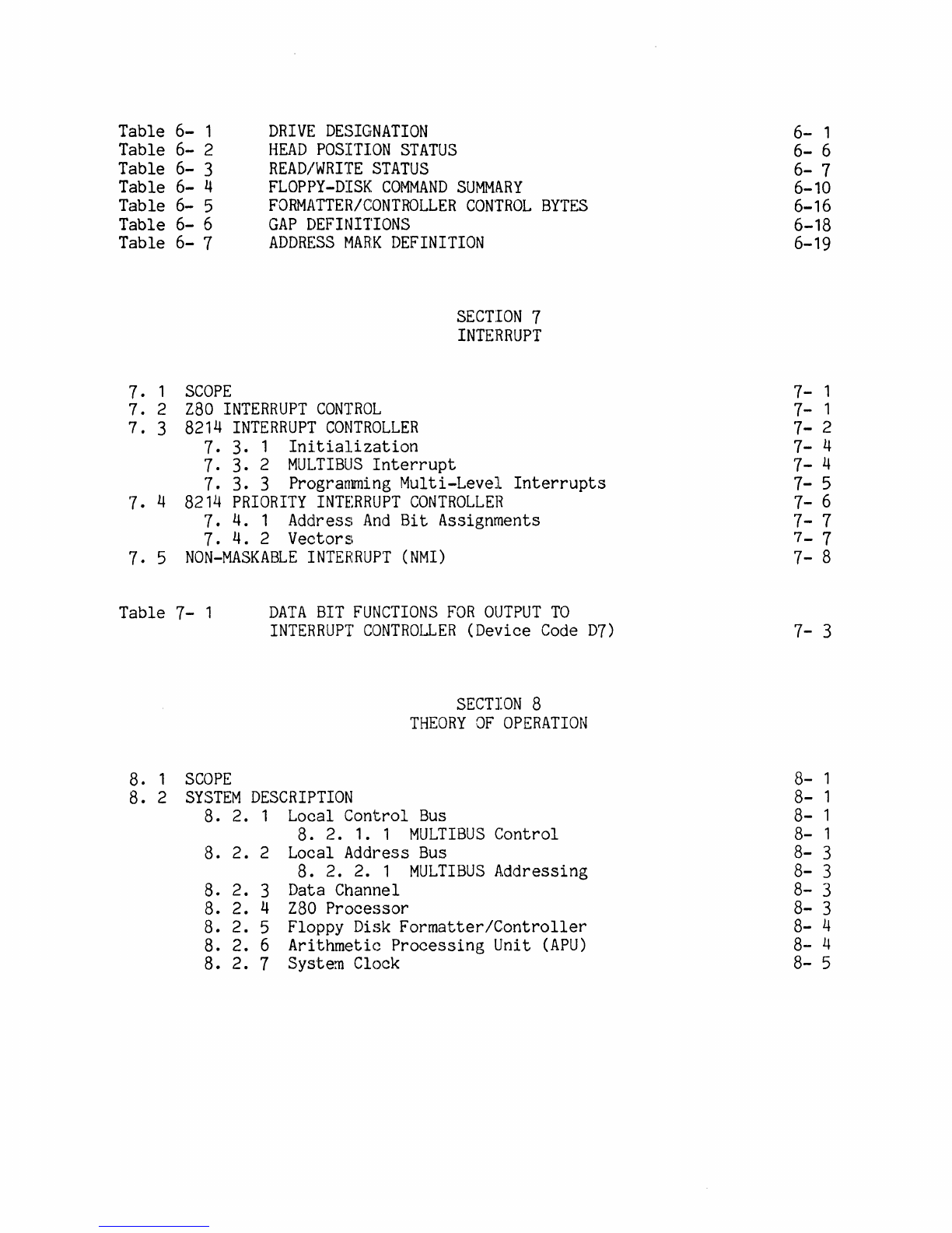
Table
6-
1
Table
6-
2
Table 6- 3
Table
6-
4
Table 6- 5
Table 6- 6
Table
6-
7
7. 1
SCOPE
DRIVE
DESIGNATION
HEAD
POSITION
STATUS
READ/WRITE
STATUS
FLOPPY-DISK
COMMAND
SUMMARY
FORMATTER/CONTROLLER
CONTROL
BYTES
GAP
DEFINITIONS
ADDRESS
MARK
DEFINITION
SECTION
7
INTERRUPT
7.
2
Z80
INTERRUPT
CONTROL
7.
3
8214
INTERRUPT
CONTROLLER
7. 3. 1
Initialization
7. 3. 2
MULTIBUS
Interrupt
7. 3. 3 Progranming Multi-Level
Interrupts
7. 4
8214
PRIORITY
INTERRUPT
CONTROLLER
7. 4. 1 Address
And
Bit
Assignments
7. 4. 2 Vectors
7. 5
NON-MASKABLE
INTEHRUPT
(NMI)
Table
7-
1
DATA
BIT
FUNCTIONS
FOR
OUTPUT
TO
INTERRUPT
CONTROU.ER
(Device
Code
D7)
8.
1
SCOPE
8. 2
SYSTEM
DESCRIPTION
SECTION
8
THEORY
OF
OPERATION
8. 2. 1 Local Control
Bus
8. 2. 1. 1
MULTIBUS
Control
8. 2. 2 Local Address
Bus
8. 2. 2. 1
MULTIBUS
Addressing
8. 2. 3 Data Channel
8. 2. 4
Z80
Processor
8. 2. 5 Floppy Disk
Formatter/Controller
8. 2. 6 Arithmetio Processing Unit
(APU)
8. 2. 7 System Clock
6-
1
6-
6
6- 7
6-10
6-16
6-18
6-19
7-
1
7- 1
7-
2
7-
4
7-
4
7- 5
7- 6
7- 7
7-
7
7-
8
7- 3
8-
1
8-
1
8-
1
8-
1
8- 3
8- 3
8- 3
8- 3
8-
4
8- 4
8-
5

8. 3
SYSTEM
OPERATION
8. 3. 1 Wait Operation
8. 3
..
1. 1
Watchdog
Timer
8. 3. 2
OP
Fetch Cycle
8. 3. 3
Memory
Read
Or
Write
8.
3.
3. 1 Address Decoding
8. 3. 4
1/0
Cycles
8. 3.
4.
1 Arithmetic Processor Cycles
8. 3. 5 Disk
Formatter/Controller
8. 3.
5.
1
Register
Selection
8. 3. 5. 2 Clock
Circuit
8. 3. 5. 3 Data Exchange
8. 3.
5.4
Disk
Read
8. 3. 5. 5 Disk Write
8. 3.
5.
6
Head
Loading Delay
8. 3. 6 Acknowledge Cycle
8. 3. 7
Interrupt
Request
8. 3. 7. 1 Non-Maskable
Interrupt
8. 3. 8
HALT
Request
8. 3. 9 System Reset
8. 4
SYSTEM
CONTROL
8. 4. 1
Bus
State
Machine
8. 4. 1
..
1
Bus
Exchange
8. 4. 2
Memory
State
Machine
Figure
8-
1
Table 8- 1
Table
8-
2
9. 1
SCOPE
8. 4. 2. 1 Refresh
Z80
MICROPROCESSOR
CLOCK
RATE
CONFIGURATION
SYSTEM
CONTROL
PROM
SIGNAL
IDENTIFICATION
SECTION
9
ARITHMETIC
PROCESSOR
UNIT
g. 2
CAPABILITIES
9. 2. 1 I/O Addressing
9. 3
9511
ARITHMETIC
PROCESSOR
UNIT
9. 3. 1
Initialization
9. 3. 2 Stack Control
9. 3. 3 Data Format
9. 3. 3. 1
Command
Format
9. 3. 3. 2
Status
Register
9.
3.
3. 3
Floating
Point Format
8-
6
8-
6
8-
6
8- 7
8- 7
8- 8
8- 8
8-
8
8-
9
8-
9
8-10
8-10
8-10
8-11
8-11
8-12
8-12
8-12
8-13
8-15
8-15
8-15
8-16
8-17
8-17
8-
2
8-
5
8-14
9- 1
9-
1
Q-
1
9-
2
9- 2
9- 2
9- 2
9- 4
9-
4
9- 5

9. 4
9511
INSTRUCTIONS
9. 4. 1 Data
And
Stack Manipulation Operations
g. 4. 2 16-Bit F:ixed-Point Operations
9. 4. 3 32-Bit F:ixed-Point Operations
9. 4. 4 32-Bit
Floating-Point
Primary Operations
9. 4. 5 32-Bit
Floating-Point
Derived Operations
9. 5
9511
OP
CODE
FORM1\T:S
9. 6
9512
ARITHMETIC
PROCESSOR
UNIT
9. 6. 1 Stack Control
9. 6. 1. 1
Double
Precision
9. 6. 2
Co~~and
Format
9. 6. 3
Status
Register
9. 7
9512
INSTRUCTIONS
9. 7. 1 Data
And
Stack Manipulation Operations
9. 7. 2 Single
Precision
Operations
9. 7. 3.
Double
Precision
Operation
9. 8
9512
OP
CODE
FORMLATS
Figure
9-
1
Table
9-
1
Table 9- 2
Table 9- 3
Appendix A
Appendix B
Appendix C
Appendix D
303-0271-000
305-0271-000
9511
INITIALIZATION
SEQUENCE
STACK
CONFIGURATIONS
STATUS
BIT
DEFINITION
STACK
CONFIGURATIONS
APPENDICES
MSC
8009
PIN
ASSIGNMENT
MSC
8009
JUMPER
REQUIREMENT
FLOPPY-DISK
JUMPER
CONFIGURATION
9511
APPLICATION
NOTE
DRAWINGS
MSC
8009
BOARD
LAYOUT
MSC
8009
SCHEMATIC
9- 6
9- 7
9-
8
9- 8
9- 9
9- 9
9-14
9-34
9-34
9-35
9-35
9-36
9-38
9-39
9-40
9-40
9-43
9- 3
9-10
9-37
9-41

SECTION
'1
INTRODUCTION
1.1
SCOPE
The
Monolithic Systems Corporation
MSC
8009
is
a
single-board
OEM
computer
that
is
dlirectly
compatible with
the
industry
standard
MULTIBUS*
.
As
software development
is
a major
cost
of
any
computer
system,
the
8080
software
compatibility
of
the
MSC
8009
provides
an
advanced, high-speed,
next-generation
system without
incurring
the
costs
and
delays
associatedl with developing
new
software.
New
systems can
now
be designed
taking
full
advantage
of
the
Z80A*
instruction
set
and
optional
floating-point
arithmetic
unit.
The
MSC
8009
operates
in a multimaster system with
either
parallel
or
serial
priority
resolution.
An
on-board bus
plus
the
MULTIBUS
structure
allows
other
operations
to
proceE~d
on
the
MULTIBUS
while
the
Z80A
processor
uses
local
memory
and
1/0
devices.
Since
the
on-board
memory
and
1/0
resources
are
extensive,
bus access
is
usually
needed only
for
communication between
tasks.
System throughput with
multiple
masters
is
greatly
enhanced because
of
the
light
MULTI
BUS
traffic
load.
MULTIBUS
compatibility
means
that
the
MSC
8009
can
be
used
either
to
expand
existing
SBC
80-based systems or as
the
basis
of
a
new
design.
An
on-board
floppy-disk
formatter/controller
in
addition
to
two
serial
ports
will
increase'
the
computing
power
for
most
applications.
Via a
17q3
Floppy-Disk
FormatterlController,
the
floppy-disk
interface
of
the
MSC
800Q
offers
a
soft-sector
format
that
can
be
made
IBM
compatible
with
the
proper softw'are. Variable
length
sectors
and
the
self-clocking
feature
of
the
1793
means
more
data
per
track.
The
system uses
Z80
block
1/0
instructions
to
transfer
data.
Write pre-compensation reduces
error
rate;
and
the
data
separator
is
crystal
controlled.
Programmable
stepping
rates
from 3
to
15
milliseconds
lets
the
MSC
8009
operate
with
drives
having
different
track-to-track
access time.
*MULTIBUS
is
a
registered
trademark
of
Intel
Corporation
Z80A
is
a
registered
trademark
of
Zilog
Inc.
100-0123-001
1-1

1.2
SPECIFICATIONS
PROCESSOR:
Z80A
(4
MHz)
MULTIBUS
COMPATIBILITY:
Full
MULTIBUS
control
logic
permits
up
to
16
bus masters
(including
other
MSC
CPU's)
to
share
the
system
bus.
BUS
EXCHANGE
MODES:
Three bus
modes
allow exchange
of
bus master every
cycle,
every
instruction
(allows
test
and
set),
or
never.
The
program
sets
the
bus
modes
for
optimum
control
of
multi-processing
systems.
CYCLE
TIME:
The
execution
of
the
fastest
Z80A
instruction
require
1.25
microseconds.
FLOPPY
DISK
INTERFACE:
Format:
Accomodates
single-
and
double-density
formats
that
are
compatible with
IBM
soft-sector
configuration.
Read
Mode:
Single/multiple
sector
read with automatic
search
or
entire
track
read.
Either
selectable
128
byte
or
variable
length
sector.
Write
Mode:
Single/multiple
sector
write
with automatic
search.
Entire
track
write
capability
for
diskette
formatting.
Supporting Software:
CP/M
100-0123-001
1-2

o
o
I
o
--"
£\.)
W
I
o
I 0
W
9511
FLOATING
POINT
AlU
8214
INT[RRUPT
CONTROllER
&
yrCTOR
PR(JIt
rlOPPV
D[',!'
[10
r:ONNF
r.
TOR
!len
rlOPPY
O[<:;K
CONTROllER
DIV
IOrR
STAT[
MACHINE
~.[
RIAL
1/0
CONNfnOR
8253
TIMER
lJSART
i
l80
n!
PROCESSOR
MUl
TIRUS™
MSC
8009
MICROCOMPfm'~R
<;[RJAI
J10
r.o~mF
r.
TOR
USART
CLOCK
16MHI
DYNAMIC
RAM
32K
ROM/EPROM
4K,
BK,
16K
or
3
MSC
8009
1M I MU..T J
BUS
I S A
~EG
I
STEREO
TRACE.'HARK
0-
T~
INTEL
CCRPCJ<Arr~
180
IS
A
REGISTERED
TRAOCr~
CF
n£
1ilOG
INC.

Capability:
With proper
drive
options,
up
to
eight
4-
or
8-inch
disk
drives
intermixed can
be
controlled.
Model
Compatibility:
The
models
listed
can be accommodated. However,
other
drives
can be used
and
have
not
been
included.
MEMORY
CAPACITY:
Shugart
SA-400
Shugart
SA-450
Shugart
SA-800
Shugart
SA-850
RAM
-
32K
bytes,
dynamic
EPROM
-
The
MSC
8009
is
shipped with four
sockets
that
accomodate
most
8-bit
wide
memory
devices
with
standard
24-pin
callout.
Capacities
include:
1)
To
32K
using
8K
x 8
masked-ROM
elements.
2)
To
16K
using
4K
x 8
EPROM
elements.
3)
To
8K
using
2K
x 8
EPROM
elements.
4)
To
4K
using
1K
x 8
EPROM
elements.
MEMORY
MANAGEMENT:
RAM
and
ROM
addressing
under
PROM
control
Dual-address
map
option
provides
two,
selectable
under program
control.
on
1K-byte
boundaries.
complete
address
maps
MEMORY
PROTECTION:
A
protection
PROM
allows
the
selection
of
system
resources
that
are
available
to
other
MULTIBUS
masters.
Any
or
all
of
the
RAM,
ROM
or
1/0
subsystems
may
be
protected
from
external
access.
MEMORY
REFRESH:
The
memory
refresh
cycles
are
automatic
and
nearly
transparent.
100-0123-001
1-4

DIRECT
MEMORY
ACCESS:
Another bus
mastE~r
may
access
the
on-board
memory
or
1/0
devices
(if
allowed
by
the
protection
PROM)
:in
625
to
750
nanoseconds.
FLOATING
POINT
ARITHt1ETIC:
Two
optional
Arithmetic Processing Units
are
available
--
the
9511
and
the
9512
..
The
9511
provides
32-bit
precision
fixed or
floating
point
operations
including
transcendental
functions.
For
increased
performance,
the
9512
offers
32-
and
64-bit
arithmetic
operations.
INTERRUPTS:
Vectored,
8-levels
of
priority
interrupts
plus
Non-Maskable
Interrupt
(NMI).
All on-board
interrupt
sources
are
open
collector
so
that
a
number
of
devices can
share
the
same
level.
Two
serial
ports
provide a programmable
interface
that
can be used
for
either
synchronous or asynchronous
operation.
One
port
can be
configured
for
Ed
ther
EIA
RS-232-C,
TTL
or
opto-isolated
20
mA
loop
signals.
The
other
port
can be configured
for
EIA
RS-232-C
or
TTL
only.
Signal
specifications
are:
Synchronous:
5-
to
8-hit
character;
one or
two
programmable
SYNC
characters.
Asynchronous
::
5-
to
8-bit
character;
1,
1-1/2,
or
2
stop
bits;
choice
of
parity
or
error
detection.
BAUD
Rates:
75
through
9600
BAUD,
software
selectable.
100-0123-001
1-5

TIMERS:
One
16-bit
counter/timer
with
six
operational
modes.
MODE
0 -
Interrupt
MODE
1 - Programmable/Retriggerable
One-shot
MODE
2 - Pulse Rate Generator
MODE
3 - Squarewave Generator
MODE
4 - Software Triggered Strobe
MODE
5 -
Hardware
Triggered Strobe
MODE
6 -
Baud
Rate Generator
for
one
serial
port
INTERFACE
SIGNALS:
MULTIBUS:
All
signals
conform with
MULTIBUS
specifications.
Floppy Disk
1/0:
All
signals
are
TTL
compatible.
Serial
1/0:
Signals
fulfill
either
EIA
RS-232-C,
TTL
or
20
rnA
current
loop
convention depending
on
the
MSC
8009
configuration.
Interrupt
Requests:
All
signals
are
TTL
compatible.
Timer:
All
signals
are
TTL
compatible.
POWER
REQUIREMENTS:
The
MSC
8009
operates
with
MULTIBUS
power
supply voltages
of
+5V,
-5V,
+12V,
and
-12V.
100-0123-001
1-6

PHYSICAL
DIMENSIONS:
12
in.(Width) X 6.75
in.(Height)
X
0.5
in.(Depth).
1.3
FUNCTIONAL
DESCRIPTION
The
MSC
8009
design
is
based
on
the
Z80A
microprocessor,
which
is
fully
upward
compatible with
the
popular
8080A.
The
Z80A
executes
all
8080
instructions
without
mJdification.
In
fact,
there
are
cases
where
8080
progr
ams
in
ROM
and
PROM
can simply
be
plugged
into
the
MSC
8009
with a
significant
improvement
in
performance. However,
care
must be taken
when
certain
programming techniques have been used
in
8080
application
programs due
to
the
4-MHz
clock
rate
of
the
Z80A.
Polling
loops
or
delay-timing
routines
may
require
adjustment.
An
additional
flag
appears
in
the
flag
register
for'
the
BCD
subtraction
feature.
Flag
differences
may
be
sign:ificant
in
rar'e
cases
where
uncommon
programming
techniques have been employed.
1.4
Z80A
PROCESSOR
The
Z80A
processor
itself
offers
features
that
are
beyond
those
of
the
8080
or
8085.
The
designer or programner can use
these
features
to
reduce system
size
or
further
increase
the
speed
of
application
programs. These
features
include:
(1)
80
additional
instructions
(2)
Double
compliment
of
registers
(3) Block
transfer
1/0
instructions
(4) Index
registers
(5)
BCD
subtraction
(6)
Two
additional
interrupt
modes
(7)
Non-Maskable
Interr'upt
(NMI)
(8) Block
search
and
block
move
instructions
100-0123-001
1-7

1.5
ARITHMETIC
PROCESSING
UNIT
(Optional)
The
MSC
800Q
will
accept
one
of
two
available
Arithmetic Processor Units
(APU) •
1
.5.
1
9511
APU
The
9511
enhances
the
computational
capability
of
the
MSC
8009.
It
is
capable
of
performing
32-bit
operations
using
floating
point
as
well
as
fixed-point
data
formats. Data
transfers
are
to
or
from
an
internal
stack.
Commands
are
issued
to
a second
1/0
address
to
perform
an
operation
on
the
data
that
is
contained
in
this
stack.
The
status
of
the
9511
can
be
read
out
at
any
time from
the
same
1/0
address.
The
results
are
then
made
available
for
retrieval,
or
an
additional
command
may
be
entered.
If
the
9511
is
busy,
it
will
cause
the
Z80
to
wait
if
the
CPU
tries
to
access
the
9511.
Some
of
the
arithmetic
and
transcendental
functions
in
addition
to
control
and
conversion
commands
that
can
be
performed with
the
9511
include:
1.5.2
9512
APU
(1) Basic Arithmetic Operations (Addition"
Subtraction,
Multiplication
and
Division).
(2) Trigonometric
Functions.
(3) Logarithmic Functions
(Common
and
Natural).
(4)
Constant Pi ('It) -y'
(5)
Exponential Functions (e
~
or
X
).
(6) Stack Control
(single,
double
or
floating).
(1)
Square Root.
(8)
Change
Signs
(single,
double or
floating).
The
9512
provides
single-precision
(32-bit)
and
double-precision
(64-bit)
add,
subtract,
multiply
and
divide
operations.
All operand
result,
status
and
command
information
transfers
take
place over
an
8-bit
bidirectional
data
bus. Using
programmed
I/O,
the
user can handle
all
data
transfers
between
the
Z80
and
the
9512. Operands
are
pushed
onto
an
internal
stack
by
the
Z80;
and
a
command
is
issued
to
perform
an
operation
on
the
data
stack.
By
popping
the
stack,
the
final
result
is
then
made
available
to
the
Z80.
100-0123-001
1-8

1.6
BUS
INTERFACE
The
MSC
8009
uses
an
internal
bus
for
access
to
the
on-board
memory,
arithmetic
processor,
floppy-disk
formatter/controller
and
I/O. Since
these
on-board
tasks
do
not
require
the
MULTIBUS,
the
MSC
8009
is
able
to
perform
internal
operations
and
not
interfere
with
the
MULTIBUS
activities.
This
means
that
up
to
16
bus masters
(including
other
MSC
8009'
s)
can share'
thE~
MULTIBUS
and
provide
the
user
with
the
benefits
of
multiprocessing.
1.7
MODE
STATUS
REGISTER
An
internal
8-bit
register
sets
up
the
MSC
8009
via
software
control
for
the
following
indicated
modes
of
operation.
~I_O_7~~IO_6
__
+-I_O~
I~~IO_3
____
~_02
__
~
______
IOO
__
MEMORY
HAP
INTERRUPT
MODE
1.7.1
Bus
Exchange
Modes
INTERRUPT
PRIORITY
BUS
EXCHANGE
MODE
Through program
control,
the
user
can use
bits
4
and
5 (104
and
105)
to
select
one
of
three
bus
modes
for
optimum
control
of
a
multiprocessing
system. These
modes
are:
105
104
0 0
0
X
X =
don't
care
BUS
OPERATION
Bus
released
to
higher
priority
on
every
data
transfer.
Bus
exchange only
on
M1
processor
cycle
(Fetch
Instruction).
MSC
8009
keeps
the
bus.
100-0123-001
1-9

1.8
READ/WRITE
MEMORY
In
the
basic
system,
the
dual-ported
dynamic
RAM
provides
the
MSC
8009
with
up
to
32K-byte
storage
capacity_
The
sixteen-chip
memory
array
is
partitioned
into
two, 16K-byte
sections.
Either
the
address
lines
of
the
Z80A
processor
or
the
MULTIBUS
(Direct
Memory
Access) address
these
arrays.
The
refresh
cycle
of
the
dynamic
RAM
is
automatic.
So
that
requested
memory
operations
can
be
performed with
minimum
time
delay,
the
refresh
cycle
is
hidden.
1.8.1
Refresh Cycle
If
either
a
memory
read
or
write
operation
of
the
dynamic
RAM
is
in
progress,
the
refresh
cycle
is
inhibited.
When
the
memory
cycle
is
complete, a
refresh
cycle
may
be
initiated.
The
refresh
control
logic
attempts
to
initiate
a
refresh
during
an
M1
machine
cycle,
making
the
refresh
transparent.
However,
if
an
M1
cycle
is
not
available,
the
refresh
is
still
inserted.
1.9
READ
ONLY
MEMORY
Four
ROM/EPROM
sockets
accommodate
the
most popular
8-bit
wide, 24-pin
memory
devices.
These devices normally hold
the
commonly
used
subroutines,
standard
support software
and
programs
for
specific
applications.
By
using
the
2108
and
2158
(1K
X
8EPROM),
the
MSC
8009
can hold
up
to
4K
bytes
of
program
storage.
The
2516
or
2116
(2K
X 8
EPROM)
provides
8K
bytes
while
either
the
2532
or
2132
4K
X8
EPROM
offers
the
user
16K
bytes.
For
32K
byte
capacity,
the
user can use
the
8K
X 8
masked
ROMs.
Since each
ROM/EPROM
device
may
vary
in
power
configuration,
hardware
jumpers provide
the
required
voltages.
Different
chips
may
be
intermixed,
but
three
of
the
four
sockets
must
contain
the
same
devices.
For example,
standard
support software
may
require
three
2116's
(2K
X 8
EPROM)
and
one
8K
X 8
Masked
ROM
--
total
capacity
of
14K
bytes.
1.9.1
Protection
PROM
A
special
PROM
protects
any
or
all
RAM,
ROM
or
I/O subsystems from
external
access.
This device
generates
an
internal
enabling
signal
that
permits
the
bus
to
address
the
MSC
8009
only
when
called
for.
Apin
on
the
auxilliary
connector
totally
disables
access
to
the
MSC
8009
board,
allowing
multiple
processors
to
be
paged
into
the
same
memory
space.
100-0123-001
1-10

1.10
DUAL
MAP
CONFIGURATION
(Optional)
The
optional
DUAL
MAP
feature
provides
the
MSC
B009
with
two
complete
address maps.
The
system always powers
up
using
the
first
map.
Since
the
system has
to
have a
ROM
at
location
zero
to
start
properly,
a
ROM
should
be
mapped
into
low
memory.
For example,
the
user
can switch
to
a
map
that
contains
RAM
in
low
memory.
This
is
achieved through a
bit
sent
with
the
same
output
instruction
used
for
programming
the
interrupt
controller
(See paragraph
1.7).
A "0"
in
bit
position
six
represents
a
s
tart
up
condition
:,
and
a "
1"
switches
the
map.
This capabi
Ii
ty
permits
the
use
of
soft.ware
written
for
BOBO
and
ZBOA
processors
that
previously
could not
be
run
on
a
single-board
computer.
1.11
I/O
INTERFACE
Two
serial
110
interfaces
provide
the
MSC
B009
with
serial-data
communication channels
that
are
programmable
and
will
operate
either
synchronously
or
asynchronously based
on
the
current
serial-data
transmission
protocols.
The
floppy
disk
interface
can support
up
to
eight
soft-sector
drives.
Since
an
address
decoder
PROM
defines
the
MSC
BOOQ
address
structure,
any
1/0
device on-board
may
be
assigned any
of
the
256
device address codes used
by
the
BOBO
or
ZBOA
instruction
set.
1.11.1
Serial
110
Interfaces
The
two
serial
110
interfaces
are
designed around
two
software-programmable devices
--
an
8251
USART
(Universal/Asynchronous
Receiver/Transmitter)
and
an
B253
Prograrrnnable Timer.
The
user can
configure
one channel only for
either
EIA
RS-232-C,
TTL
or
opto-isolated
20
rnA
current-loop
operation.
The
other
channel can
be
configured
for
either
EIA
RS-232-C
or
TTL
operation.
NOTE:
For
current
loop
operation,
supplies
the
current
source
for
the
external
device
proper
operation.
The
user'
s
progr~am
selects
the
mode
of
operation,
data
format,
control
character
format,
par:L
ty
and
BAUD
rate.
The
B251
provides
full
duplex,
double-buffered
transmit
and
receive
capabilities.
Also,
parity,
overrun
and
framing
error
detection
are
incorporated
within
the
USART.
One
section
of
the
B2~)3
supplies
the
BAUD
rate
clock under program
control
to
all
channels
optionally
or
additional
sections
can
be
used
for
different
baud
rates
on
the
other
serial
channels.
100-0123-001
1-11
Table of contents
Other MSC Motherboard manuals