Note
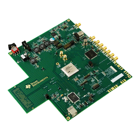
SYNCA, SYNCB, and SYNCC SMAs are used to provide external SYNC signals from the FPGA. The
cables of each SYNC signal should have equal length to ensure the signal arrives at the same time for
all boards using these SYNCs. The TRIG IN SMA connector can be used to trigger the FPGA from an
external source. All four SMAs use 3V3 logic CMOS signals. The EVM has onboard translators to set
these inputs/outputs to the correct voltage levels for the FPGA.
3.3.3.2 FPGA Mezzanine Card (FMC+) Connector
The TSW14J58 EVM has one connector to allow for the direct plug in of TI JESD204C_B serial interface
ADC and DAC EVMs. The specifications for this connector are mostly derived from the ANSI/VITA 57.4 FPGA
Mezzanine Card (FMC+) Standard. This standard describes the compliance requirements for a low-overhead
protocol bridge between the IO of a mezzanine card and an FPGA processing device on a carrier card. This
specification is being used by FPGA vendors on their development platforms.
The FMC+ connector, J3, provides the interface between the TSW14J58EVM and the ADC or DAC EVM under
test. This 560-pin Samtec high-speed, high-density connector (part number ASP-184329-01) is suitable for
high-speed differential pairs up to 32.5 Gbps.
In addition to the JESD204B/C standard signals, several CMOS single-ended signals and LVDS differential
signals are connected between the FMC+ and FPGA. In the future, these signals may allow the HSDC Pro GUI
to control the SPI serial programming of ADC and DAC EVMs that support this feature. The connector pinout
description is shown in Table 3-5.
Table 3-5. FMC+ Connector Description of the TSW14J58
FMC+ Signal Name FMC+ Pin Standard JESD204 Application
Mapping
Description
RXP/N0_0 C6 and C7 Lane 0± (M → C) JESD Serial data transmitted from mezzanine and received by carrier
RXP/N1_0 A2 and A3 Lane 1± (M → C) JESD Serial data transmitted from mezzanine and received by carrier
RXP/N2_0 A6 and A7 Lane 2± (M → C) JESD Serial data transmitted from mezzanine and received by carrier
RXP/N3_0 A10 and A11 Lane 3± (M → C) JESD Serial data transmitted from mezzanine and received by carrier
RXP/N0_1 A14 and A15 Lane 4± (M → C) JESD Serial data transmitted from mezzanine and received by carrier
RXP/N1_1 A18 and A19 Lane 5± (M → C) JESD Serial data transmitted from mezzanine and received by carrier
RXP/N2_1 B16 and B17 Lane 6± (M → C) JESD Serial data transmitted from mezzanine and received by carrier
RXP/N3_1 B12 and B13 Lane 7± (M → C) JESD Serial data transmitted from mezzanine and received by carrier
RXP/N0_2 B8 and B9 Lane 8± (M → C) JESD Serial data transmitted from mezzanine and received by carrier
RXP/N1_2 B4 and B5 Lane 9± (M → C) JESD Serial data transmitted from mezzanine and received by carrier
RXP/N2_2 Y10 and Y11 Lane 10± (M → C) JESD Serial data transmitted from mezzanine and received by carrier
RXP/N3_2 Z12 and Z13 Lane 11± (M → C) JESD Serial data transmitted from mezzanine and received by carrier
RXP/N0_3 Y14 and Y15 Lane 12± (M → C) JESD Serial data transmitted from mezzanine and received by carrier
RXP/N1_3 Z16 and Z17 Lane 13± (M → C) JESD Serial data transmitted from mezzanine and received by carrier
RXP/N2_3 Y18 and Y19 Lane 14± (M → C) JESD Serial data transmitted from mezzanine and received by carrier
RXP/N3_3 Y22 and Y23 Lane 15± (M → C) JESD Serial data transmitted from mezzanine and received by carrier
TXP/N0_0 C2 and C3 Lane 0± (C → M) JESD Serial data transmitted from carrier and received by mezzanine
TXP/N1_0 A22 and A23 Lane 1± (C → M) JESD Serial data transmitted from carrier and received by mezzanine
TXP/N2_0 A26 and A27 Lane 2± (C → M) JESD Serial data transmitted from carrier and received by mezzanine
TXP/N3_0 A30 and A31 Lane 3± (C → M) JESD Serial data transmitted from carrier and received by mezzanine
TXP/N0_1 A34 and A35 Lane 4± (C → M) JESD Serial data transmitted from carrier and received by mezzanine
TXP/N1_1 A38 and A39 Lane 5± (C → M) JESD Serial data transmitted from carrier and received by mezzanine
TXP/N2_1 B36 and B37 Lane 6± (C → M) JESD Serial data transmitted from carrier and received by mezzanine
TXP/N3_1 B32 and B33 Lane 7± (C → M) JESD Serial data transmitted from carrier and received by mezzanine
TXP/N0_2 B28 and B29 Lane 8± (C → M) JESD Serial data transmitted from carrier and received by mezzanine
TXP/N1_2 B24 and B25 Lane 9± (C → M) JESD Serial data transmitted from carrier and received by mezzanine
TXP/N2_2 Z24 and Z25 Lane 10± (C → M) JESD Serial data transmitted from carrier and received by mezzanine
TXP/N3_2 Y26 and Y27 Lane 11± (C → M) JESD Serial data transmitted from carrier and received by mezzanine
TXP/N0_3 Z28 and Z29 Lane 12± (C → M) JESD Serial data transmitted from carrier and received by mezzanine
www.ti.com Hardware Configuration
SLWU094 – MARCH 2021
Submit Document Feedback
TSW14J58 JESD204C Data Capture and
Pattern Generator Card
9
Copyright © 2021 Texas Instruments Incorporated
