MSI MS-5148 User manual


CHAPTER 1 INTRODUCTION
1-1
Chapter 1
Introduction
The PCI 430 TX system board is a high-performance personal computer
system board based on a 3.3v version of the PentiumTM micrprocessor--the
P54C and P55C, K6 and M2 with MMX microprocessor. The system board
supports the Peripheral Component Interconnect (PCI) Local Bus Standard
and provide four 32-bit PCI bus master slots.
A cache subsystem can be configured for 256k or 512K cache memory to
improve overall throughput.
The system board uses the highly integrated Intel 82439TX chipset to
support the PCI/ISA and green standards, and to provide the Host/PCI
bridge. The 82437AB chipset also support the ACPI soft power off and
Modem Ring wake-up function, it also integrates all system control func-
tions.

CHAPTER 1 INTRODUCTION
1-2
1.1 System Board Features
CPU
lSocket 7 supports Intel PentiumTM family--P54CandP55C((MMX)
90MHz/100MHz/120Mhz/133MHz/150MHz/166MHz/200MHz/233MHz
lThe Cyrix 6x86/M2 and AMD K5/K6 are also supported.
Chip Set
lIntel 82430TX
Cache Memory
lSupports Directed Map Organization,Write-Back cache policy.
lSupports 256K pipelined burst cache memory or 512K pipelined burst
cachememory.
Main Memory
lSupports six memory banks using four 72-pin SIMM sockets and two 168-
pin DIMM sockets.
lUp to 256 Mbytes main memory.
lSupports EDO Hyper Page Mode DRAM , Standard Fast Page mode
DRAMandSDRAM.
Slots
lFour 32-bit Master PCI Bus slots and four 16-bit ISA bus slots. One
shared slot that can be used as ISA or PCI.
lSupport3.3VPCIAdd-OnCard.
On-Board Peripherals
lOn-BoardPeripheralsinclude:
- 1 floppy port supports 2FDD
-2serialports(COMA+COMB)
- 1 parallel port supports ECP or EPP mode
- 2 PCI Bus Master IDE ports (up to four IDE HDD)
- 2 Channel USB port

CHAPTER 1 INTRODUCTION
1-3
Dimensions
lStandard ATX form factor
l30cm(L)x18.6cm(W)x4layerPCB
Mounting
l6 mounting holes

CHAPTER 1 INTRODUCTION
1.3 System Board Layout
MS-5148
SIMM1
SIMM2
SIMM3
SIMM4
DIMM1
DIMM2
Socket 7
FDD
IDE1
IDE2
ISA SLOT 4
ISA SLOT 2
ISA SLOT 3
ISA SLOT 1
PCI SLOT 4
PCI SLOT 3
PCI SLOT 2
PCI SLOT 1
BIOS
BATT
+
2032
JPF
JGS
JGL
JP2
INTEL
FW82371AB
INTEL
FW82439TX
JBAT JRMS2
JFAN
ATX
POWER CONNECTOR
KBC
IR
JV1
LPT
COMA & COMB USB PS/2
JV3
JV4
JV5
SW
ON DIP
12
134
156
JV6
JRMS1
+
1-4

CHAPTER 2 HARDWARE INSTALLATION
CPU
CPU
OpenLever
Pin1
Sliding
Plate
White dot/
Cut edge
Close
Lever
Chapter 2
Hardware Installation
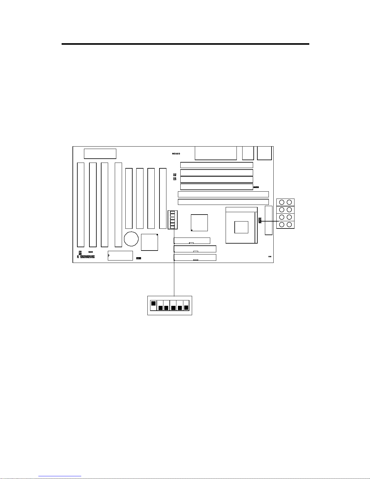
2.1 Central Processing Unit: CPU
The430 TX motherboard operates withIntel®P54C/P55C,Cyrix®6x86/
M2andAMD®5K86/K6processors. It could operates with 2.8V to 3.52V
processors. The motherboard provides a 321-pin ZIF Socket 7 for easy CPU
installation, a DIP switch (SW1) to set the proper speed for the CPU and a
Jumper block (JV3 - JV7) for setting the CPU voltage. The CPU should
always have a cooling fan attached to prevent overheating.
2-1
1. Pull the lever sideways away
from the socket then raise
the lever up to a 90-degree
angle.
3. Press the lever down to
complete the installation.
2. Locate Pin 1 in the socket
and look for the white dot or
cut edge in the CPU, match
Pin 1 with the white dot/cut
edge then insert the CPU. It
should insert easily.
2.1-1 CPU Installation Procedure

CHAPTER 2 HARDWARE INSTALLATION
1. The 3 CPU clock frequencies that the system supports are 55MHz, 60MHz,
66MHz and 75MHz (To adjust SW1 pin 4, 5, and 6 ). See the following
chart to set the different Host Clock Frequencies.
4 5 6 Clock
ON ON OFF 55MHz
ON OFF OFF 60MHz
OFF OFF OFF 66MHz
OFF ON OFF 75MHz
SW1 CPU
2. The DIP Switch SW1 (1,2, and 3) is used to set the Core/Bus (Fraction)
ratio of the CPU. The actual core speed of the CPU is the Host Clock
Frequency multiplied by the Core/Bus ratio. For example:
If CPUClock = 66MHz
Core/Bus ratio = 3/2
then CPU core speed = Host Clock xCore/Bus ratio
= 66MHzx3/2
= 100MHz
3. The PCI Bus Clock is the CPU Clock Frequency divided by 2.
2.1-2 CPU Core Speed Derivation Procedure
1 2 3 Core/BusRatio
OFF OFF OFF 1.5/3.5
ON OFF OFF 2
ON ON OFF 2.5/1.75
OFF ON OFF 3
SW1 CPU
2-2

CHAPTER 2 HARDWARE INSTALLATION
2.9
VcoreV I/O
3.38 3.38
3.52 3.52
3.3 2.8
3.3
3.3 3.2
JV3~JV7
2.1-3 CPU Voltage Setting: JV3 - JV7
The system board can autodetect whether the CPU is single or dual voltage.
To adjust the Jumper setting of the CPU’s Vcore, just look at table below and
set accordingly.
SIMM1
SIMM2
SIMM3
SIMM4
DIMM1
DIMM2
Socket 7
FDD
IDE1
IDE2
ISA SLOT 4
ISA SLOT 2
ISA SLOT 3
ISA SLOT 1
PCI SLOT 4
PCI SLOT 3
PCI SLOT 2
PCI SLOT 1
BIOS
BATT
+
2032
JPF
JGS
JGL
JP2
INTEL
FW82371AB
INTEL
FW82439TX
JBAT JRMS2
JFAN
ATX
POWER CONNECTOR
KBC
IR
JV1
LPT
COMA & COMB USB PS/2
JV3
JV4
JV5
SW
ON DIP
12
134
156
JV6
JRMS1
+
JV3
JV4
JV6
JV5
Vcore
V I/O JV3~JV7
Single Voltage Dual Voltage
2-3
JV3
JV4
JV6
JV5
JV3
JV4
JV6
JV5
JV3
JV4
JV6
JV5
JV3
JV4
JV6
JV5
JV3
JV4
JV6
JV5

CHAPTER 2 HARDWARE INSTALLATION
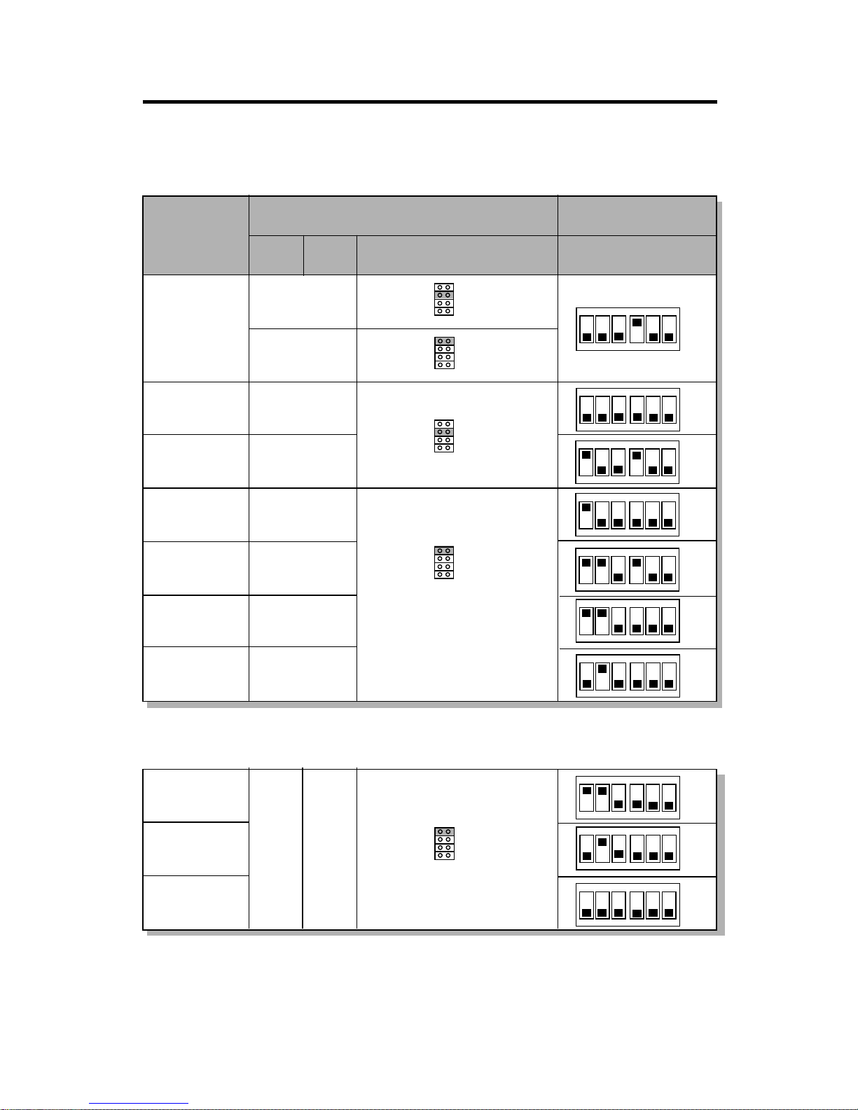
2.1-4 CPU Speed and Voltage Setting: SW1 & JV3-JV7
To adjust the speed and voltage of the CPU, you must know the specifica-
tion of your CPU (always ask the vendor for CPU specificaton) then look at
Table2.1 (Intel®P54C/P55C-MMX),Table 2.2(Cyrix®6x86/M2) and
Table2.3 (AMD®5K86/K6)forpropersetting.
SW1 1 2 3 4 5 6
ON ON
OFF
Speed Setting
2-4
SIMM1
SIMM2
SIMM3
SIMM4
DIMM1
DIMM2
Socket 7
FDD
IDE1
IDE2
ISA SLOT 4
ISA SLOT 2
ISA SLOT 3
ISA SLOT 1
PCI SLOT 4
PCI SLOT 3
PCI SLOT 2
PCI SLOT 1
BIOS
BATT
+
2032
JPF
JGS
JGL
JP2
INTEL
FW82371AB
INTEL
FW82439TX
JBAT JRMS2
JFAN
ATX
POWER CONNECTOR
KBC
IR
JV1
LPT
COMA & COMB USB PS/2
JV3
JV4
JV5
SW
ON DIP
12
134
156
JV6
JRMS1
+
JV3
JV4
JV6
JV5

CHAPTER 2 HARDWARE INSTALLATION
Table 2.1 Intel® P54C PENTIUM CPU
P54C-90
P54C-100
P54C-120
P54C-133
P54C-150
P54C-166
P54C-200
3.38
3.52
3.52
3.38
3.38
3.52
3.52
3.52
ON DIP
123 456
ON
OFF
ON DIP
123 456
ON
OFF
ON DIP
123 456
ON
OFF
ON DIP
123 456
ON
OFF
ON DIP
123 456
ON
OFF
CPU Type CPU SpeedCPU Voltage
SW1VI/O Vcore
ON DIP
123 456
ON
OFF
ON DIP
123 456
ON
OFF
2-5
JV3
JV4
JV5
JV6
JV3
JV4
JV5
JV6
JV3
JV4
JV5
JV6
JV3
JV4
JV5
JV6
JV3~JV7
ON DIP
123 456
ON
OFF
ON DIP
123 456
ON
OFF
ON DIP
123 456
ON
OFF
P55C-166
P55C-200 3.3 2.8 JV3
JV4
JV5
JV6
P55C-233
Intel® P55C PENTIUM (MMX) CPU
Note: If you encounter a CPU with different Voltage, just go to page 2-3 and
look for the proper voltage settings.

CHAPTER 2 HARDWARE INSTALLATION
Table 2.2 Cyrix® 6x86 CPU
Cyrix® 6x86 CPU uses P to rate the speed of there processor base on Intel®
CPUcorespeed,forexampleP150+ (120MHz) has 150MHz core speed of
Intel®buthas120MHzcorespeedin Cyrix®. Cyrix® 6x86 CPU should
always uses a more powerful fan (ask vendor for proper cooling fan).
3.52
ON DIP
123 456
ON
OFF
CPU Type CPU SpeedCPU Voltage
SW1VI/O Vcore
M1P133+
(110MHz)
M1P150+
(120MHz)
M1P166+
(133MHz)
ON DIP
123 456
ON
OFF
2-6
M1P200+
(150MHz)
ON DIP
123 456
ON
OFF
ON DIP
123 456
ON
OFF
3.3 2.8
3.52 JV3
JV4
JV5
JV6
JV3
JV4
JV5
JV6
JV3
JV4
JV5
JV6
JV3~JV7
ON DIP
123 456
ON
OFF
M2P166+
(166MHz)
M2P180+
(180MHz)
M2P200+
(200MHz)
ON DIP
123 456
ON
OFF
M2P225+
(225MHz)
ON DIP
123 456
ON
OFF
3.3 2.8 JV3
JV4
JV5
JV6
ON DIP
123 456
ON
OFF
Cyrix® M2 (MMX) CPU
Note: We don’t guarantee the performance of 75MHz Bus Clock.

CHAPTER 2 HARDWARE INSTALLATION
Table 2.3 AMD® 5K86 CPU
AMD® 5K86 CPU uses PR to rate the speed of there processor base on
Intel®CPUcore speed ,forexample PR133+ (100MHz) has133MHzcore
speed of Intel® but has 100MHz core speed in AMD® 5K86 CPU.
ON DIP
123 456
ON
OFF
3.52
ON DIP
123 456
ON
OFF
123 456
CPU Type CPU SpeedCPU Voltage
SW1
VI/O Vcore
PR100
(100MHz)
PR120
(90MHz)
ON DIP
123 456
ON
OFF
2-7
PR133
(100MHz)
JV3~JV7
JV3
JV4
JV5
JV6
PR90
(90MHz)
PR150
(105MHz)
PR166
(116.7MHz)
PR200
(133MHz) Reserved
ON DIP ON
OFF
ON DIP ON
OFF
ON DIP ON
OFF
ON DIP
123 456
ON
OFF
3.3 ON DIP
123 456
ON
OFF
PR200
(200MHz)
PR233
(233MHz)
ON DIP
123 456
ON
OFF
JV3
JV4
JV5
JV6
PR166
(166MHz) 2.9
AMD® K6 (MMX) CPU
3.3 3.2 JV3
JV4
JV5
JV6
Note: If you encounter a CPU with different Voltage, just go to page 2-3 and
look for the proper voltage settings.

CHAPTER 2 HARDWARE INSTALLATION
2.1-5 CPU Fan Power Connector: JFAN
This connector supports CPU cooling fan with +12V. It supports both two
and three pin head connector. When connecting the wire to the connector,
always take note that the red wire is the positive and should be connected to
the +12V. If the system is in suspend mode, the fan will stop. You can change
this setup on thePower Management Setup in the BIOS.
JFAN
Connector
+12V
GND GND
Recommended CPU cooling fan specification:
- Metallic Clip
- RPM5000
- CFM 10
- +12V
- 52x52x10mm
- BallBearing
Note: Always consult vendor for
proper CPU cooling fan.
2-8
SIMM1
SIMM2
SIMM3
SIMM4
DIMM1
DIMM2
Socket 7
FDD
IDE1
IDE2
ISA SLOT 4
ISA SLOT 2
ISA SLOT 3
ISA SLOT 1
PCI SLOT 4
PCI SLOT 3
PCI SLOT 2
PCI SLOT 1
BIOS
BATT
+
2032
JPF
JGS
JGL
JP2
INTEL
FW82371AB
INTEL
FW82439TX
JBAT JRMS2
JFAN
ATX
POWER CONNECTOR
KBC
IR
JV1
LPT
COMA & COMB USB PS/2
JV3
JV4
JV5
SW
ON DIP
12
134
156
JV6
JRMS1
+

CHAPTER 2 HARDWARE INSTALLATION
2.2 Flash ROM Programming Voltage: JP2
This jumper is for setting the Voltage of the Flash ROM BIOS.
13 13
+12V +5V
(default)
Voltage Setting
1
JP4
3
SIMM1
SIMM2
SIMM3
SIMM4
DIMM1
DIMM2
Socket 7
FDD
IDE1
IDE2
ISA SLOT 4
ISA SLOT 2
ISA SLOT 3
ISA SLOT 1
PCI SLOT 4
PCI SLOT 3
PCI SLOT 2
PCI SLOT 1
BIOS
BATT
+
2032
JPF
JGS
JGL
JP2
INTEL
FW82371AB
INTEL
FW82439TX
JBAT JRMS2
JFAN
ATX
POWER CONNECTOR
KBC
IR
JV1
LPT
COMA & COMB USB PS/2
JV3
JV4
JV5
SW
ON DIP
12
134
156
JV6
JRMS1
+
JP2
2-9
22
Note: a. If you use Winbond , SST Flash ROM short 1-2 pin.
b. If you use Intel or MXIC Flash ROM short 1-2 pin, if you want to
flash the ROM data, short 2-3 pin , then put it back to 1-2 pin.

CHAPTER 2 HARDWARE INSTALLATION
123
2.3 External Battery Connector: JBAT
A battery must be used to retain the system board configuration in CMOS
RAM. If you use the on-board battery you must short pins 1,2 of JBAT to
keep the CMOS data.
JBAT
12
SIMM1
SIMM2
SIMM3
SIMM4
DIMM1
DIMM2
Socket 7
FDD
IDE1
IDE2
ISA SLOT 4
ISA SLOT 2
ISA SLOT 3
ISA SLOT 1
PCI SLOT 4
PCI SLOT 3
PCI SLOT 2
PCI SLOT 1
BIOS
BATT
+
2032
JPF
JGS
JGL
JP2
INTEL
FW82371AB
INTEL
FW82439TX
JBAT JRMS2
JFAN
ATX
POWER CONNECTOR
KBC
IR
JV1
LPT
COMA & COMB USB PS/2
JV3
JV4
JV5
SW
ON DIP
12
134
156
JV6
JRMS1
+
2-10
3
123
Keep Data Clear Data

CHAPTER 2 HARDWARE INSTALLATION
2.4 Power Saving Switch Connector: JGS/
Power Saving LED Connector: JGL
Attach a power saving switch to JGS. When the switch is pressed, the
system immediately goes into suspend mode. Press any key and the system
wakes up. JGL can be connected with LED to monitor the JGS.
JGS
SIMM1
SIMM2
SIMM3
SIMM4
DIMM1
DIMM2
Socket 7
FDD
IDE1
IDE2
ISA SLOT 4
ISA SLOT 2
ISA SLOT 3
ISA SLOT 1
PCI SLOT 4
PCI SLOT 3
PCI SLOT 2
PCI SLOT 1
BIOS
BATT
+
2032
JPF
JGS
JGL
JP2
INTEL
FW82371AB
INTEL
FW82439TX
JBAT JRMS2
JFAN
ATX
POWER CONNECTOR
KBC
IR
JV1
LPT
COMA & COMB USB PS/2
JV3
JV4
JV5
SW
ON DIP
12
134
156
JV6
JRMS1
+
JGL
2-11

CHAPTER 2 HARDWARE INSTALLATION
SIMM1(Bank 0)
SIMM2(Bank 0)
SIMM3(Bank 1)
SIMM4(Bank 1)
2-12
SIMM1
SIMM2
SIMM3
SIMM4
DIMM1
DIMM2
Socket 7
FDD
IDE1
IDE2
ISA SLOT 4
ISA SLOT 2
ISA SLOT 3
ISA SLOT 1
PCI SLOT 4
PCI SLOT 3
PCI SLOT 2
PCI SLOT 1
BIOS
BATT
+
2032
JPF
JGS
JGL
JP2
INTEL
FW82371AB
INTEL
FW82439TX
JBAT JRMS2
JFAN
ATX
POWER CONNECTOR
KBC
IR
JV1
LPT
COMA & COMB USB PS/2
JV3
JV4
JV5
SW
ON DIP
12
134
156
JV6
JRMS1
+
DIMM1(Bank 2)
DIMM2 (Bank 3)
2.5 Memory Installation
2.5-1 Memory Bank Configuration
The system board provides four 72-pin SIMMs (Single In-Line Memory Mod-
ule) and two 168-pin DIMM(Double In-Line Memory) sockets, supports a
maximumof256MBofmemory. You can use SIMM from 4MB, 8MB, 16MB,
32MB,64MBor128MB. AndDIMMfrom8MB,16MB,32MB,64MB, 128MB,
or 256MB. A Bank consist of 2 SIMM socket or One DIMM socket. It also
consist of 2 RAS, each RAS supports memory up to 128MB.This board sup-
port 6 RAS.

CHAPTER 2 HARDWARE INSTALLATION
2.5-2 Memory Installation Procedures:
1. The SIMM slot has a “Plastic Safety
Tab” and the SIMM memory module
has a “Notched End”, so the SIMM
memory module can only fit in one
direction.
2. Insert the SIMM memory modules into
the socket at 45-degree angle, then
push into a vertical position so that it
will snap into place.
3. The Mounting Holes and Metal Clips
should fit over the edge and hold the
SIMM memory modules in place.
A. HowtoinstallaSIMMModule
Single Sided SIMM
Double Sided SIMM
Notched
End
2-13

CHAPTER 2 HARDWARE INSTALLATION
B. HowtoinstallaDIMMModule
1. The DIMM slot has a two key mark “VOLT and DRAM” , so the
DIMM memory module can only fit in one direction.
2. Insert the DIMM memory module vertically into the DIMM slot
then push it in.
3. Close the plastic clip at the side of the DIMM slot.
SingleSidedDIMM
DoubleSidedDIMM
Note:If you have installed SIMM and DIMM at the same time. You must
use a 3.3 volt DIMM with 5 volt I/O signal tolerance or a full 5 volt
DIMMmodule(EDO,FPorSDRAM). LookforJV1toselectthe
DIMM voltage.
2-14

CHAPTER 2 HARDWARE INSTALLATION
2-15
B.1 DIMMPowerVoltageSelector : JV1
DIMMVoltage JV1
5V
3.3V
SIMMPowerLevel:5Volts DIMMPowerLevel: 3.3Vor5V
SIMM1
SIMM2
SIMM3
SIMM4
DIMM1
DIMM2
Socket 7
FDD
IDE1
IDE2
ISA SLOT 4
ISA SLOT 2
ISA SLOT 3
ISA SLOT 1
PCI SLOT 4
PCI SLOT 3
PCI SLOT 2
PCI SLOT 1
BIOS
BATT
+
2032
JPF
JGS
JGL
JP2
INTEL
FW82371AB
INTEL
FW82439TX
JBAT JRMS2
JFAN
ATX
POWER CONNECTOR
KBC
IR
JV1
LPT
COMA & COMB USB PS/2
JV3
JV4
JV5
SW
ON DIP
12
134
156
JV6
JRMS1
+
JV1
+5V
+3V
Table of contents
Other MSI Motherboard manuals

MSI
MSI MS-7293 Series User manual

MSI
MSI 945G Neo User manual

MSI
MSI MAG X570S TORPEDO MAX User manual
MSI
MSI MS-6135 User manual
MSI
MSI 848P Neo2-V Series User manual

MSI
MSI K9MM-V User manual

MSI
MSI Z270 TOMAHAWK ARCTIC User manual

MSI
MSI MICRO NLX BX4 User manual

MSI
MSI B250M BAZOOKA PLUS User manual

MSI
MSI MS-6378 Instruction manual

MSI
MSI MS-98H5 User manual

MSI
MSI B450M BAZOOKA V2 User manual

MSI
MSI B650M GAMING PLUS WIFI User manual

MSI
MSI KT4A-V User manual

MSI
MSI MS-6334 User manual

MSI
MSI B660-A PRO DDR4 User manual

MSI
MSI H410I PRO WIFI User manual

MSI
MSI Q35MDO v2 User manual

MSI
MSI X58A-GD65 series User manual

MSI
MSI MS-5156 User manual