Absolute Maximum Ratings (Notes 1,
2)
If Military/Aerospace specified devices are required,
please contact the National Semiconductor Sales Office/
Distributors for availability and specifications.
V (SW, FB, R1- 2, G1-2,
B1-2) pins:
Voltage to GND (Notes 3, 4) −0.3V to +7.2V
V
DD1
,V
DD2
,V
DD_IO
−0.3V to +6.0V
Voltage on Logic Pins –0.3V to V
DD_IO
+0.3V, with 6.0V max
I (R1, G1, B1, R2, G2, B2)
(Note 5) 150 mA
I(V
REF
)10µA
Continuous Power Dissipation
(Note 6) Internally Limited
Junction Temperature (T
J-MAX
) 125˚C
Storage Temperature Range −65˚C to +150˚C
Maximum Lead Temperature
(Reflow soldering, 3 times)
(Note 7) 240˚C
ESD Rating (Note 8)
Human Body Model: 2 kV
Machine Model: 200V
Operating Ratings (Notes 1, 2)
V (SW, FB, R1-2, G1-2, B1-2) 3.0V to 6.0V
V
DD1
,V
DD2
(Note 4) 2.65V to 2.9V
V
DD_IO
1.8V to V
DD1,2
Recommended Load Current 0 mA to 300 mA
Junction Temperature (T
J
) Range −40˚C to +125˚C
Ambient Temperature (T
A
) Range
(Note 9) −40˚C to +85˚C
Thermal Properties
Junction-to-Ambient Thermal Resistance (θ
JA
),
SQA24A Package (Note 10) 39˚C/W
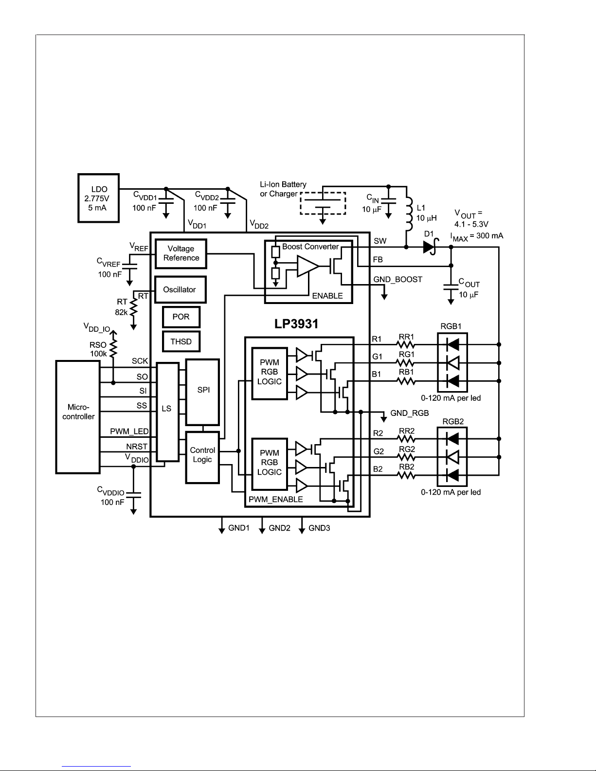
Electrical Characteristics (Notes 2, 11)
Limits in standard typeface are for T
J
= 25˚C. Limits in boldface type apply over the operating ambient temperature range
(−40˚C ≤T
J
≤+85˚C). Unless otherwise noted, specifications apply to the LP3931 Typical Application Circuit (pg. 1) with: V
DD1
=V
DD2
=V
DDIO
= 2.775V, C
VDD1
=C
VDD2
=C
VDDIO
= 0.1 µF, C
OUT
=C
IN
= 10 µF, C
VREF
= 0.1 µF, L
1
= 10 µH, R
T
= 82k
(Note 12).
Symbol Parameter Condition Min Typ Max Units
I
DD
Standby Supply Current
(V
DD1
and V
DD2
current)
NSTBY = L (register)
SCK, SS, SI, NRST = H 15µA
No-Load Supply Current
(V
DD1
and V
DD2
current, boost off)
NSTBY = H (reg.)
EN_BOOST = L (reg.)
SCK, SS, SI, NRST = H
170 250 µA
Full Load Supply Current
(V
DD1
and V
DD2
current, boost on)
NSTBY = H (reg.)
EN_BOOST = H (reg.)
SCK, SS, SI, NRST = H
All Outputs Active
1mA
I
DD_IO
V
DD_IO
Standby Supply Current NSTBY = L (reg.)
SCK, SS, SI, NRST = H 1µA
V
DD_IO
Supply Current 1 MHz SCK Frequency
C
L
=50pFatSOPin 20 µA
V
REF
Reference Voltage (Note 13) I (V
REF
)≤1 nA,
Test Purposes Only
1.205
−2
1.23 1.255
+2
V
%
Note 1: Absolute Maximum Ratings indicate limits beyond which damage to the component may occur. Operating Ratings are conditions under which operation of
the device is guaranteed. Operating Ratings do not imply guaranteed performance limits. For guaranteed performance limits and associated test conditions, see the
Electrical Characteristics tables.
Note 2: All voltages are with respect to the potential at the GND pins (GND1-3, GND_BOOST, GND_RGB).
Note 3: Battery/Charger voltage should be above 6V no more than 10% of the operational lifetime.
Note 4: Voltage tolerance of LP3931 above 6.0V relies on fact that VDD1 and VDD2 (2.775V) are available (ON) at all conditions. If VDD1 and VDD2 are not available
(ON) at all conditions, National Semiconductor does not guarantee any parameters or reliability for this device.
Note 5: The total load current of the boost converter should be limited to 300 mA.
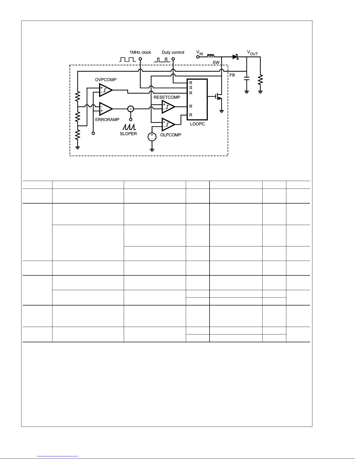
Note 6: Internal thermal shutdown circuitry protects the device from permanent damage. Thermal shutdown engages at TJ= 160˚C (typ.) and disengages at TJ=
140˚C (typ.).
Note 7: For detailed package and soldering specifications and information, please refer to National Semiconductor Application Note 1187: Leadless Leadframe
Package (LLP).
Note 8: The Human body model is a 100 pF capacitor discharged through a 1.5 kΩresistor into each pin. The machine model is a 200 pF capacitor discharged
directly into each pin. MIL-STD-883 3015.7.
LP3931
www.national.com 4