NXP Semiconductors MFRC52 Series Guide

AN1445
Antenna design guide for MFRC52x, PN51x and PN53x
Rev. 1.2 — 11 O
ctober 2010
144512
Application note
PUBLIC
Document information
Info Content
Keywords NFC, MFRC522, MFRC523, PN511, PN512, PN531, PN532, Antenna
Design, RF Design, constant current design
Abstract This application notes provides guidance on antenna and RF design for
NFC devices MFRC522, MFRC523, PN511, PN512, PN531, PN532

NXP Semiconductors
AN1445
Antenna design guide for MFRC52x, PN51x and PN53x
AN1445_12
All information provided in this document is subject to legal disclaimers.
© NXP B.V. 2010. All rights reserved.
Application note
PUBLIC
Rev. 1.2 — 11 October 2010
144512
2 of 65
Contact information
For additional information, please visit: http://www.nxp.com
For sales office addresses, please send an email to: salesaddresses@nxp.com
Revision history
Rev
Date
Description
1.2
20101011
Update with MFRC522 and MFRC523
1.1
2008/02/22
Selection Guide and all topologies added
1.0
2007/10/31
Initial Release

NXP Semiconductors
AN1445
Antenna design guide for MFRC52x, PN51x and PN53x
AN1445_12
All information provided in this document is subject to legal disclaimers.
© NXP B.V. 2010. All rights reserved.
Application note
PUBLIC
Rev. 1.2 — 11 October 2010
144512
3 of 65
1. Introduction
1.1 Purpose and Scope
This application note is intended to give a practical guide to design and dimension
antennas and RF parts for contactless reader as well as NFC devices. The application
note will provide the required understanding to design application specific antennas and
dimensioning RF parts to achieve the best performance for a communication according
to the different communication schemes of the ICs.
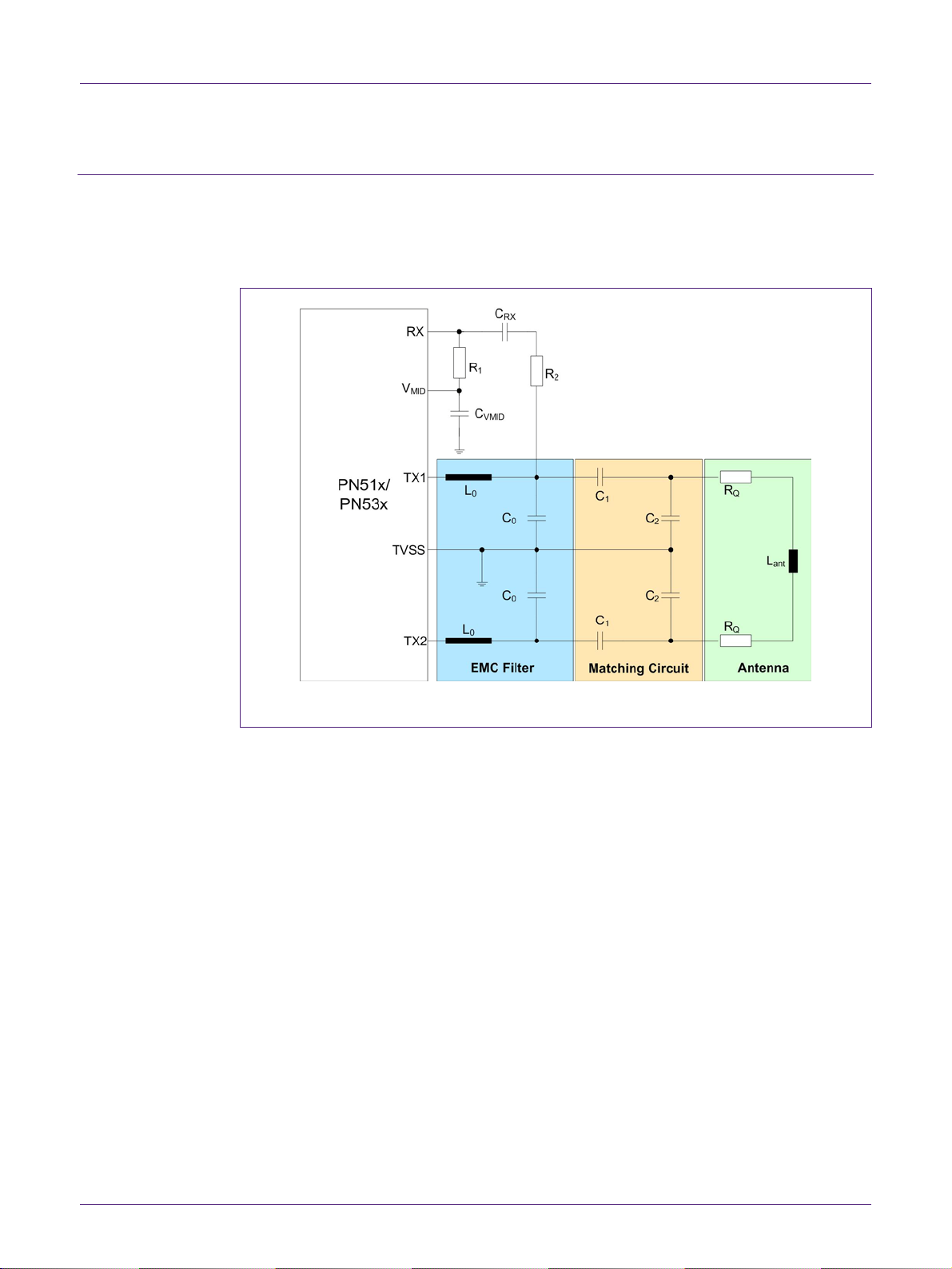
The RF part covers the required matching circuit to match an application specific antenna
coil to the output driver of the MFRC522/MFRC523/PN51x/PN53x as well as the
receiving circuit in order to detect a received RF signal.
1.2 MFRC52x/PN51x/PN53x features
The MFRC522/MFRC523/PN51x/PN53x devices are designed to communicate in three
different operation modes:
1. Reader/Writer mode to communicate to an ISO/IEC14443A, MIFARE card up to
100 mm depending on the antenna size and tuning. (MFRC52x /PN51x/PN53x).
2. Reader/Writer mode to communicate to a ISO/IEC14443 B card up to 100 mm
depending on the antenna size and tuning (MFRC523/PN51x/PN53x).
3. Reader/Writer mode to communicate to a FeliCa card up to 100 mm depending on
the antenna size and tuning (PN51x, PN53x).
4. NFCIP-1 mode to communicate to another NFC devices up to 100 mm depending on
the antenna sizes and tuning (PN51x, PN53x).
5. ISO/IEC14443A, MIFARE card or FeliCa card mode to communicate to
ISO/IEC14443A, MIFARE or FeliCa reader up to 100 mm depending on the
generated external field strength. (PN51x, PN53x)
The MFRC52x/PN51x/PN53x’s overall functionality can be separated into three
functions:
6. Generate the RF field: The generated magnetic field has to be maximized within the
limits of the transmitter supply current and general emission limits.
7. Transmit data: The coded and modulated data signal has to be transmitted in a way,
that every card and MFRC52x /PN51x/PN53x device is able to receive it. The signal
shape and timing according to relevant standards has to be considered.
8. Receive data: The response of a card or MFRC52x /PN51x/PN53x device has to be
transferred to the receive input of the PN51x/PN53x considering various limits, e.g.
maximum voltage and receiver sensitivity.
The operating distance for the MFRC52x/PN51x/PN53x depends on
•the matching of the antenna,
•the sensitivity of the receiving part,
•the antenna size of the device,
•the antenna size of the communication partner and
•external parameters, such as metallic environment and noise.

NXP Semiconductors
AN1445
Antenna design guide for MFRC52x, PN51x and PN53x
AN1445_12
All information provided in this document is subject to legal disclaimers.
© NXP B.V. 2010. All rights reserved.
Application note
PUBLIC
Rev. 1.2 — 11 October 2010
144512
4 of 65
Note: MFRC52x devises are Reader/Writer devises only. So these are not able to
operate in target mode.
2. How to use this document
The application note is intended to give a practical guide to choose the matching
topology, to design antennas and calculate the matching components for the
MFRC52x/PN51x/PN53x RF part. It gives a guideline starting with the recommended RF
matching circuitry description as well as a dedicated description of the transmitter
matching resistance and matching procedure in each chapter. The appendix of this
document provides an introduction in the overall antenna design theory for the system.
Depending on the target applications, different design decisions can be made in order to
optimize the antenna topology. The environmental constraints of a device/antenna are
the influencing detuning parameters for the RX-path and have to be investigated.
Conditions for a detuning are determined by the type of an application and housing, e.g.
peer-to-peer mode, card mode, metal or composite plastic housing. These effects can
cause large voltage drops at the RX-site and therefore may affect demodulation of the
signal.
The user needs to follow the selection guide in chapter 3 to choose
the appropriate antenna topology!
This application note is outlined as followed
1. Antenna Selection Guide
2. Antenna Topology I
3. Antenna Topology II
4. Adoptions of Antenna Topology I or II
5. Antenna Topology III
6. Appendix
a. The appendix includes information describing the calculation of the
inductance of an antenna coil and gives basic hints on symmetry and
environmental influences. The calculation of the equivalent circuits and an
overview of all relevant formulas are give as well as Tips and hints to check the
antenna and RF part design.
Each Antenna Topology provides information about
a. The RF part block diagram. It shows a recommended circuitry design with all
relevant components required to connect an antenna to the PN51x/PN53x. It also
ensures the transmission of energy and data to the target device as well as the
reception of a target device answer.
b. The TX matching resistance Rmatch is explained which is required to calculate the
remaining components and to optimize PN51x/PN53x power consumption.

NXP Semiconductors
AN1445
Antenna design guide for MFRC52x, PN51x and PN53x
AN1445_12
All information provided in this document is subject to legal disclaimers.
© NXP B.V. 2010. All rights reserved.
Application note
PUBLIC
Rev. 1.2 — 11 October 2010
144512
5 of 65
c. Formulas to calculate the EMC filter and the matching circuit
d. Antenna tuning procedure
e. Design and calculation of the receiving part
f. Example calculations
Note: This application note does not replace the relevant datasheets referenced in
chapter 9.
“Card” in this document means a contactless smart card according to the
ISO/IEC14443A (or MIFARE) or a contactless card according to the FeliCa
scheme. Design hints on how to place the components on a PCB are not included.
Tuning and measurement of the antenna has always to be performed at the final
mounting position to consider all parasitic effects, e.g. metal influence on quality
factor, inductance and additional capacitance.
All topologies and design methods described in this document assume
antenna and tuning components are not accessible to end user. Therefore
no additional ESD protection methods are described. In case antenna wiring
is accessible from device housing or after user removable parts are
detached, additional ESD protection has to be evaluated. Methods described
here are then no more generally valid.
Increased RF output power and communication distance could be achieved
by integrating the RF amplifier for NXP’s contactless Reader IC’s ([13]).

NXP Semiconductors
AN1445
Antenna design guide for MFRC52x, PN51x and PN53x
AN1445_12
All information provided in this document is subject to legal disclaimers.
© NXP B.V. 2010. All rights reserved.
Application note
PUBLIC
Rev. 1.2 — 11 October 2010
144512
6 of 65
3. Selection Guide
The following flow chart describes a selection guide for different antenna topologies. The
user needs to start from the top rectangle going downwards. Due to different detuning
effects on the antenna only one of the following topologies may apply to the type of
reader integration.
Antenna Topology I
Antenna Topology II
Asymmetric antenna tuning
according to chapter 6
Antenna Topology III
Verify detuning at RX-Path
according to chapter 4.6
“Receiver Circuit Design”
MIFARE, Type-A/B, FeliCa,
Peer-to-Peer
If communication problems occur, that
can not be resolved by adjusting register
settings or RX-path dimensioning,
Antenna Topology II needs to be
applied.
This is the starting point of the selection
guide. This means, all indicated
protocols can be supported by the
following antenna topologies.
Antenna Topology II resolves strong
detuning effects on the matching
circuit.
Antenna Topology III has the same
physical constraints as the asymmetric
tuning of the recent topologies. Antenna
Topology III requires less matching
components.
If Antenna Topology I and II cannot
counteract communication errors in
certain distances, the EMC filter and
matching circuit has to be adjusted
according to chapter 6
It is recommended to start with Antenna
Topology I since this is the basis for
possible further adoptions.

NXP Semiconductors
AN1445
Antenna design guide for MFRC52x, PN51x and PN53x
AN1445_12
All information provided in this document is subject to legal disclaimers.
© NXP B.V. 2010. All rights reserved.
Application note
PUBLIC
Rev. 1.2 — 11 October 2010
144512
7 of 65
4. Antenna Topology I
The RF block diagram in Fig 1 shows a recommended circuitry design with all relevant
components required to connect an antenna to the MFRC522/MFRC523/PN51x/PN53x.
It also ensures the transmission of energy and data to the target device as well as the
reception of a target device answer.
Fig 1. Block diagram of the complete RF part
Note: Fig 1 shows only the RF part and the related power supply (TVDD and TVSS). For
a proper operation the analog and digital supplies and the host interface have to
be connected too.
Note: Topology I is the preferred RF part topology for MFRC522 and MFRC523
Although some of theses blocks may contain only a few passive components, it is
important to consider all these blocks and all their functionality to guarantee the proper
working of the complete device.
The EMC filter reduces 13.56 MHz harmonics and performs an impedance
transformation.
The Matching Circuit acts as an impedance transformation block.
The antenna coil itself generates the magnetic field.
The receiving part provides the received signal to the
MFRC522/MFRC523/PN51x/PN53x internal receiving stage.
Basically this complete RF circuitry consists of at least 8 capacitors (max. voltage ~50V
types), 2 inductors, 2 resistors (the part size determines the maximum power which the
resistor can withstand) and the symmetrical antenna coil as shown in Fig 1.

NXP Semiconductors
AN1445
Antenna design guide for MFRC52x, PN51x and PN53x
AN1445_12
All information provided in this document is subject to legal disclaimers.
© NXP B.V. 2010. All rights reserved.
Application note
PUBLIC
Rev. 1.2 — 11 October 2010
144512
8 of 65
4.1 Equivalent circuit
The following subchapters describe the matching procedure. It starts with the
determination of the antenna parameters and ends with a fine tuning of the antenna
circuitry.
4.1.1 Determination of series equivalent circuit
The antenna loop has to be connected to an impedance or network analyzer to measure
the series equivalent components.
Note: The equivalent circuit (see Fig 2) must be determined under final environmental
conditions especially if the antenna will be operated in metal environment or a
ferrite will be used for shielding.
Antenna
Ra
La
Ca
Fig 2. Series equivalent circuit
Typical values:
La= 0.3...3 µH
Ca= 3...30 pF
Ra= 0.3...8 Ω
4.1.2 Calculation of antenna quality factor damping resistor RQ
The quality factor of the antenna is calculated with
a
a
aR
L
Q
⋅
=
ω
If the calculated value of Qais higher than the target value of 35, an external damping
resistor RQhas to be inserted on each antenna side to reduce the Q-factor to a value of
35 (±10%).
The value of RQ(each side of the antenna) calculates as
−
⋅
⋅= a
a
QR
L
R35
5.0
ω
4.1.3 Determination of parallel equivalent circuit
The parallel equivalent circuit of the antenna together with the added external
damping resistor RQhas to be measured. The quality factor should be checked again to
be sure to achieve the required value of Q=35.
(1)
(2)

NXP Semiconductors
AN1445
Antenna design guide for MFRC52x, PN51x and PN53x
AN1445_12
All information provided in this document is subject to legal disclaimers.
© NXP B.V. 2010. All rights reserved.
Application note
PUBLIC
Rev. 1.2 — 11 October 2010
144512
9 of 65
Note: The equivalent circuit (Fig 3) must be determined under final environmental
conditions especially if the antenna will be operated in metal environment or a
ferrite will be used for shielding.
Antenna
R
Q
R
Q
R
pa
L
pa
C
pa
Fig 3. Parallel equivalent circuit
The following formula applies
Qa
a
pa
apa
apa
RR L
R
CC
LL
⋅+
⋅
=
=
=
2)(
ˆ
ˆ
ˆ
2
ω
4.2 EMC filter design
The EMC filter circuit for the MFRC522/;MFRC523/PN51x/PN53x fulfills two functions:
the filtering of the signal and impedance transformation block. The main properties of the
impedance transformation are:
•Decreasing the amplitude rise time after a modulation phase
•Increasing the receiving bandwidth
The EMC filter and the matching circuit must transform the antenna impedance to the
required TX matching resistance Zmatch(f) at the operating frequency of f = 13.56 MHz.
Fig 4. Impedance transformation
When splitting the circuit between EMC Filter and Matching Circuit the following applies if
instead of the IC two resistors with the value Rmatch/2 would be applied:
(3)

NXP Semiconductors
AN1445
Antenna design guide for MFRC52x, PN51x and PN53x
AN1445_12
All information provided in this document is subject to legal disclaimers.
© NXP B.V. 2010. All rights reserved.
Application note
PUBLIC
Rev. 1.2 — 11 October 2010
144512
10 of 65
Fig 5. Definition of transformation impedance Ztr
trtrtr jXRZ +=
trtrtr jXRZ −=
*
EMC filter general design rules:
L0= 390 nH - 1 µH
Filter resonance frequency fr0 = 14.1 MHz ...14.5 MHz, => C0
( )
0
2
0
02
1
Lf
C
r
⋅⋅
=
π
The EMC filter resonance frequency fr0 has to be near the upper sideband frequency
determined by the highest data rate (848 kHz sub carrier) in the system to achieve a
broadband receiving characteristic.
Example:
L0= 560 nH
fr0 = 14.3 MHz
C0= 221.2 pF => chosen: 220 pF
A recommended value of 560 nH for L0is chosen to calculate the capacitance C0. The
following formulas apply for Zant = Re(Zant)+Im(Zant) and are needed to calculate the
matching components.
( )
2
0
2
00
22
1
⋅⋅+⋅⋅−
=
C
R
CL
R
R
match
match
tr
ωω
(4)
(5)
(6)
(7)

NXP Semiconductors
AN1445
Antenna design guide for MFRC52x, PN51x and PN53x
AN1445_12
All information provided in this document is subject to legal disclaimers.
© NXP B.V. 2010. All rights reserved.
Application note
PUBLIC
Rev. 1.2 — 11 October 2010
144512
11 of 65
( )
( )
2
0
2
00
2
0
2
00
2
0
2
1
4
1
2
⋅⋅+⋅⋅−
⋅−⋅⋅−⋅
⋅⋅=
C
R
CL
C
R
CLL
X
match
match
tr
ωω
ω
ω
(8)

NXP Semiconductors
AN1445
Antenna design guide for MFRC52x, PN51x and PN53x
AN1445_12
All information provided in this document is subject to legal disclaimers.
© NXP B.V. 2010. All rights reserved.
Application note
PUBLIC
Rev. 1.2 — 11 October 2010
144512
12 of 65
4.3 Matching circuit design
4.3.1 Component calculation
The following formulas apply for the series and parallel matching capacitances:
+
⋅
⋅
≈
24
1
1
tr
patr
X
RR
C
ω
pa
patr
pa
C
RR
L
C⋅−
⋅
⋅
−
⋅
≈2
4
1
2
1
2
2
ω
ω
Finally, a fine tuning of the matching circuit is often necessary, since the calculated
values are based on simplified equations and the equivalent circuit values can not be
determined 100% correct.
4.4 Tuning procedure
The matching circuit elements C1and C2must be tuned to get the required matching
resistance Rmatch (Xmatch = 0) at the PN51x/PN53x TX pins. The matching impedance
Zmatch = Rmatch + jXmatch is measured with an impedance or network analyzer. The Zmatch
point between TX1 and TX2 as shown in Fig 6 is the probing point for the network
analyzer.
Fig 6. Measurement of matching impedance
The following Fig 7 shows a simulation example for the matching impedance Zmatch.
(9)
(10)

NXP Semiconductors
AN1445
Antenna design guide for MFRC52x, PN51x and PN53x
AN1445_12
All information provided in this document is subject to legal disclaimers.
© NXP B.V. 2010. All rights reserved.
Application note
PUBLIC
Rev. 1.2 — 11 October 2010
144512
13 of 65
Fig 7. Calculation of matching impedance
Fig 8 shows the smith chart simulation for Zmatch / 2:
Fig 8. Smith chart for matching impedance

NXP Semiconductors
AN1445
Antenna design guide for MFRC52x, PN51x and PN53x
AN1445_12
All information provided in this document is subject to legal disclaimers.
© NXP B.V. 2010. All rights reserved.
Application note
PUBLIC
Rev. 1.2 — 11 October 2010
144512
14 of 65
Conditions for the tuning:
Rmatch curve symmetric around the operating frequency
Xmatch curve conjugate complex symmetric around the operating frequency
Note: All tuning and measurement of the antenna always has to be performed at the final
mounting position to consider all parasitic effects like metal influence on quality
factor, inductance and additional capacitance.

NXP Semiconductors
AN1445
Antenna design guide for MFRC52x, PN51x and PN53x
AN1445_12
All information provided in this document is subject to legal disclaimers.
© NXP B.V. 2010. All rights reserved.
Application note
PUBLIC
Rev. 1.2 — 11 October 2010
144512
15 of 65
4.4.1 Tuning of series matching capacitance C1
The smith charts in Fig 9 show the matching impedance Zmatch / 2 vs. frequency.
a. Optimum C1
b. C1too low
c. C1too high
Fig 9. Smith charts for C
1
tuning
C1changes the magnitude of the matching impedance. After a change of C1the
imaginary part of Zmatch must be compensated by adjusting C2.

NXP Semiconductors
AN1445
Antenna design guide for MFRC52x, PN51x and PN53x
AN1445_12
All information provided in this document is subject to legal disclaimers.
© NXP B.V. 2010. All rights reserved.
Application note
PUBLIC
Rev. 1.2 — 11 October 2010
144512
16 of 65
4.5 Tuning of parallel matching capacitance C2
The smith charts show the matching impedance Zmatch / 2 vs. frequency.
d. Optimum C2
e. C2too low
f. C2too high
Fig 10. Smith charts for C
2
tuning
C2changes mainly the imaginary part of Zmatch.

NXP Semiconductors
AN1445
Antenna design guide for MFRC52x, PN51x and PN53x
AN1445_12
All information provided in this document is subject to legal disclaimers.
© NXP B.V. 2010. All rights reserved.
Application note
PUBLIC
Rev. 1.2 — 11 October 2010
144512
17 of 65
4.5.1 Tuning flow chart
Fig 11. Tuning flow chart
START
f
Zmax
> 13.56 MHz
Phase = 0
(+/-10°)
Phase = 0
(+/-10°)
Zmax = 40 -50 Ohm
Zmax < 40 -50 Ohm
|Z(13.56 MHz -
∆
f)| =
|Z(13.56 MHz +
∆
f)|
|Z(13.56 MHz -
∆
f)|
<
|Z(13.56 MHz +
∆
f)|
TUNING OK
Increase C0
Decrease C0
NO
Yes
Yes
Increase C2
Decrease C2
Yes
NO
NO
NO
Yes
Yes
NO
NO
Decrease C1
Increase C1
Yes
NO

NXP Semiconductors
AN1445
Antenna design guide for MFRC52x, PN51x and PN53x
AN1445_12
All information provided in this document is subject to legal disclaimers.
© NXP B.V. 2010. All rights reserved.
Application note
PUBLIC
Rev. 1.2 — 11 October 2010
144512
18 of 65
4.6 Receiver circuit design
Next step, after matching and tuning the transmitting antenna, is the design and tuning of
the receiver circuit. The investigations need to be carried out for initiator and target
mode.
Fig 12 shows the relevant components for the receiver circuit. R1and R2form a voltage
divider which has to be adjusted according to the incoming voltage levels at UC0. Both,
Initiator and target mode of the device have to be investigated, since detuning effects on
the RX path behave differently.
Fig 12. Receiver Circuit
4.6.1 Initiator mode
Predefined components:
Step 1:
CRX = 1 nF: DC blocking capacitor
Cvmid = 100 nF: Vmid decoupling capacitance
R1 = 1 kΩ: Predefined part of the voltage divider
The transmitter must be switched on in continuous wave mode and the voltage on the
EMC filter capacitance UC0 has to be measured with a low capacitance probe (< 2 pF).
Typically low capacitance probes are terminated with 50 Ohm, thus the scope
configuration has to be set correctly!
Step 2:
The voltage divider resistor R2can be calculated by:
Step 3:

NXP Semiconductors
AN1445
Antenna design guide for MFRC52x, PN51x and PN53x
AN1445_12
All information provided in this document is subject to legal disclaimers.
© NXP B.V. 2010. All rights reserved.
Application note
PUBLIC
Rev. 1.2 — 11 October 2010
144512
19 of 65
−⋅= 1
0
12 RX
C
U
U
RR
with the target value of URX = 1 Vpp (antenna not detuned)
After inserting the determined resistor R2the voltage on RX pin URX must be measured
with a low capacitance probe (< 2 pF) for continuous transmitting mode.
Step 4:
The voltage URX must not exceed the maximum value URXmax even when the antenna is
detuned by a target or passive card.
4.6.2 Target mode
The device must be placed in the test setup according to NFCIP1 test method standard.
The magnetic field has to be increased continuously and the voltage on RX checked
against the level URXmax.
Step 5:
URX < URXmax for H <= 7.5 A/m
If the voltage level on RX gets higher than the maximum value for field strength below
7.5 A/m, the resistor R2must be increased to a value that meets the specification.
4.7 Example
As an example the antenna of the PN51x/PN53x evaluation board Rev. 1.1 will be
matched to the transmitter output.
Fig 13. PN51x/PN53x evaluation board antenna
The external RF components should be tuned to a value, that ITVDD ≈50mA.
Recommended Rmatch ≈50 Ohm
The series equivalent circuit of the antenna results to:
Ra= 1.9 Ohm
Ca= 11 pF
La= 2.9 µH
The calculation for the external damping resistor results to RQ= 2.57 Ohm. The chosen
value for RQis 3.3 Ohm and results in a Q-factor slightly below 30.
(11)

NXP Semiconductors
AN1445
Antenna design guide for MFRC52x, PN51x and PN53x
AN1445_12
All information provided in this document is subject to legal disclaimers.
© NXP B.V. 2010. All rights reserved.
Application note
PUBLIC
Rev. 1.2 — 11 October 2010
144512
20 of 65
The parallel equivalent circuit of the antenna including quality factor damping resistors RQ
= 3.3 Ohm is determined with the following values:
Rpa = 7148 Ohm
Cpa = 11 pF
Lpa= 2.9 µH
The EMC filter is determined with:
L0= 560 nH
C0= 220 pF
Calculation of Ztr:
Rtr = 217 Ohm
Xtr = -58 Ohm
Calculation of the matching parts C1, C2:
C1= 19.8 pF -> 18 pF
C2= 54.1 pF ->56 pF
For further component calculations please refer to the Excel-Worksheet “Antenna
Topology I” in AN1444xx ([9]).
This manual suits for next models
4
Table of contents
Other NXP Semiconductors Antenna manuals
Popular Antenna manuals by other brands

MFJ
MFJ 1789 instruction manual

CommScope
CommScope ValuLine VHLP3 Series installation instructions

Iridium GO!
Iridium GO! WINSTKT1601 installation guide

FP Elettronica
FP Elettronica PASSY Installation and user manual

Kathrein
Kathrein K 70 57 21 04 1 Mounting instruction

Intellian
Intellian GX100NX Installation & Operation User Guide