NXP Semiconductors PN544 Guide

AN145715
PN544 Antenna Design Guide
Rev. 1.5 — 28th August 2009 Application Note
Document information
Info Content
Keywords NFC, PN544, Antenna Design, RF Design
Abstract This application notes provides guidance on antenna and RF design for
NFC device PN544.

NXP Semiconductors AN145715
PN544 Antenna Design Guide
145715 © NXP B.V. 2006. All rights reserved.
Application Note Rev. 1.5 — 28th August 2009 2 of 43
Contact information
For additional information, please visit: http://www.nxp.com
Revision history
Rev Date Description
1.0 18/02/2008 Initial Release
1.1 14/05/2008 Updates on demo board antenna default matching
1.2 27/02/2009 Update on antenna topology
1.3 12/03/2009 Minor Updates
1.4 30/06/2009 Appendix B added
1.5 28/08/2009 URX max changed to 1.7V

NXP Semiconductors AN145715
PN544 Antenna Design Guide
145715 © NXP B.V. 2006. All rights reserved.
Application Note Rev. 1.5 — 28th August 2009 3 of 43
1. 0Introduction
1.1 11B11BPurpose and scope
This application draft is intended to give a practical guide to estimate and tune antenna
components for the PN544 antenna topology. The PN544 is capable of performing
Reader/Writer (R/W) as well as target mode functionalities. This guide is not primarily
based on a strong mathematical background but on a practical approach towards PN544
antenna tuning. Therefore it is recommended to read and use this document as
described in the chapter 50H50H49H3 “Tuning Procedure”.
To get hands-on experience it is recommended to use an antenna which has
approximately the same outlines as the one used throughout this document.
This document will be adapted for upcoming versions and may contain a modification of
the following topology or even contain further antenna topologies.

NXP Semiconductors AN145715
PN544 Antenna Design Guide
145715 © NXP B.V. 2006. All rights reserved.
Application Note Rev. 1.5 — 28th August 2009 4 of 43
2. 1B1BPN544 Topology
The PN544 topology is outlined in 51H51H50HFig 1. It can be seen that only one antenna (Zant) is
used for Reader/Writer-and Card mode. The number of turns for this antenna topology
using the PN544 demo board is six.
57B56B57B56B
Fig. 1 PN544 antenna topology
The following component tolerances (maximum values) are required for an appropriate
tuning:
Component Maximum tolerance Component Maximum tolerance
L0 5% RQ5%
C0 5% Rx 5%
C1 2% R2 5%
C2a 2% CRX 5%
C2b 2% CVMID 5%
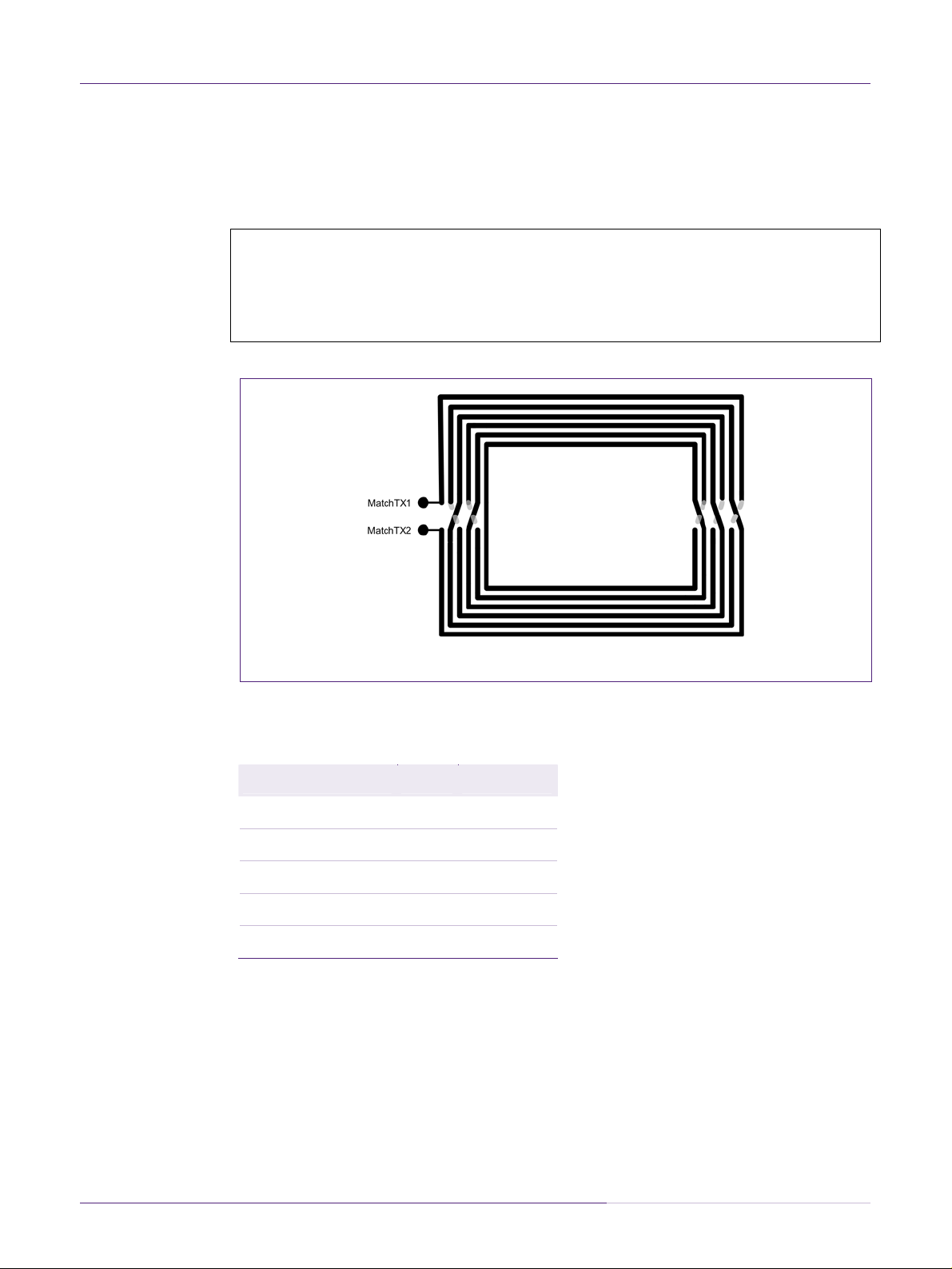
The antenna size used throughout this document is 3 cm x 5 cm. Refer also to 52H52H51HTable 1
for more details. 53H53H52HFig 2 shows the PCB-schematic of the antenna which is used in this
CRX

NXP Semiconductors AN145715
PN544 Antenna Design Guide
145715 © NXP B.V. 2006. All rights reserved.
Application Note Rev. 1.5 — 28th August 2009 5 of 43
document. The MatchTX1 and MatchTX2 points are connected to the damping resistors
Rqas well as to the capacitors C2b for the ANT1 and ANT2 pins (see also 54H54H53HFig 1).
For the sake of simplicity 55H55H54HFig 2 is a sketch of a possible PN544 demo board
antenna.
Connections MatchTX1, MatchTX2 and ANT1, ANT2 on the provided NXP PN544
demo board are routed differently.
This has no impact on the tuning procedure described.
Fig. 2 6-turn demo board antenna sketch
Antenna outlines
Physical outlines of the antenna board are shown here
description value dimensions
size 3 x 5 cm
# turns R/W 6
Copper width 0.05 cm
Spacing 0.05 cm
Copper height 35 μm

NXP Semiconductors AN145715
PN544 Antenna Design Guide
145715 © NXP B.V. 2006. All rights reserved.
Application Note Rev. 1.5 — 28th August 2009 6 of 43
3. 2B2BTuning Procedure
Please follow the steps below for tuning the antenna. The antenna is matched without
powering the PN544 IC. A detailed description of each step will follow after this chapter.
Step 1: At first the antenna has to be matched to the PN544 as described in
chapter 56H56H55H4. In this phase C2b is not assembled.
Outcome: Basic tuning with resonance frequency of 13.56MHz at 80Ohm
PN544
TX2
TX1
TVSS
VMID
RX
R1
R2
CRX
CVMID
L0
L0
C0
C0C2
C2
C1
C1
Rq
Rq
EMC
Filter
Matching
Circuit
Antenna
13.56MHz at
approximately
80Ohm
Matching circuitry and smith chart of antenna in step 1
Step 2: After tuning the antenna, C2b needs to be assembled to connect to ANT1 and
ANT2 pins. The C2 value is therefore split-up. This means if C2 is calculated and
assembled with 47pF in Step 1, then this values is split up into 20pF for C2a and 27pF
for C2b (see chapter 56H6B6BStep 4 – Card mode tuning).
Outcome: C2 splits into C2a and C2b. (By assembling C2b, the matching circuit
is now configured for card mode)
Note: The resonance frequency of the card mode is measured contactless as
described in 57HAppendix B
Block diagram with ANT1 and ANT2 connected
CRX

NXP Semiconductors AN145715
PN544 Antenna Design Guide
145715 © NXP B.V. 2006. All rights reserved.
Application Note Rev. 1.5 — 28th August 2009 7 of 43
Step 3: This step includes the validation of the Reader/Writer matching, which is
simulated by shortening the two C2b capacitors with a 10 Ohm resistor. An
asymmetric impedance curve with Rmatch=80Ohm at 13.56Mhz shall be seen on the
network analyzer. Further details on fine-tuning can be found in chapter 57H57H6.
Outcome: Asymmetric Reader/Writer tuning at 13.56MHz with Rmatch=80Ohm
Smith chart of the asymmetric Reader/Writer tuning
Step 4: By removing the 10Ohm resistor, the matching circuit is configured for card
mode. The PN544 has to be powered and configured as card. The resonance
frequency should be in the range of 14.5 to 16Mhz. Further details on tuning can be
found in chapter 58H58H58H7.
Outcome: Card tuning in between 14.5MHz to 16MHz measured with impedance
analyzer.
Attention
Step 3 and Step 4 may be repeated to find a good compromise between
Reader/Writer and card mode tuning. The target of the tuning is to find component
values such that in
•Reader/Writer mode -> Rmatch=80Ohm at 13.56Mhz
•Card mode -> fres =14.5 – 16 MHz

NXP Semiconductors AN145715
PN544 Antenna Design Guide
145715 © NXP B.V. 2006. All rights reserved.
Application Note Rev. 1.5 — 28th August 2009 8 of 43
4. 3B3BStep 1 – Antenna Matching
The RF block diagram shows the circuitry design with all relevant components required
to connect an antenna to the PN544. It also ensures the transmission of energy and data
to the target device as well as the reception of a target device answer.
Fig. 3 Block diagram of the complete RF part
59H59H59HFig 6 shows only the RF part. For a proper operation the supplies and the host interface
have to be connected
The EMC filter reduces 13.56MHz harmonics and performs an impedance
transformation.
The Matching Circuit acts as an impedance transformation block and joins the antenna
to the EMC-filter.
The Antenna coil itself generates the magnetic field.
The RX path provides the signal to the PN544 internal receiving stage.
R2 R
x

NXP Semiconductors AN145715
PN544 Antenna Design Guide
145715 © NXP B.V. 2006. All rights reserved.
Application Note Rev. 1.5 — 28th August 2009 9 of 43
4.1 12B12BEquivalent circuit
The following subchapters describe the matching procedure. It starts with the
determination of the antenna parameters and ends with a fine tuning of the antenna
circuitry.
4.1.1 26B26BDetermination of series equivalent circuit
The antenna loop has to be connected to an impedance or network analyzer to measure
the series equivalent components.
The equivalent circuit (see 60H60H60HFig 7) must be determined under final environmental
conditions especially if the antenna will be operated in metal environment or a
ferrite will be used for shielding.
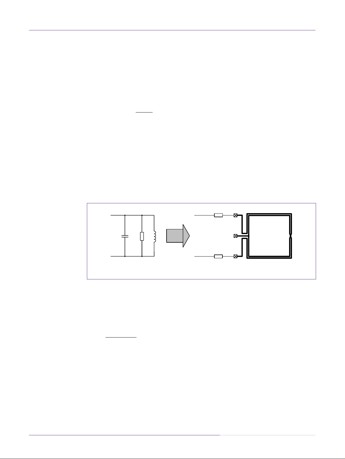
Antenna
Ra
La
Ca
Fig. 4 Series equivalent circuit
Typical values:
La= 0.3...3µH
Ca= 3...30pF
Ra= 0.3...8Ω
fra = self-resonance frequency of the antenna
The antenna capacitance Cacan be calculated with:
()
ara
aLf
C2
2
1
⋅⋅
=
π
The antenna parasitic capacitance Ca should be kept low to achieve a self-resonance
frequency > 35 MHz.
4.1.2 27B27BCalculation of damping resistor RQ
The quality factor of the antenna is calculated with
a
a
aRL
Q⋅
=
ω
(1)

NXP Semiconductors AN145715
PN544 Antenna Design Guide
145715 © NXP B.V. 2006. All rights reserved.
Application Note Rev. 1.5 — 28th August 2009 10 of 43
If the calculated value of Qais higher than the target value of 35, an external damping
resistor RQhas to be inserted on each antenna side to reduce the Q-factor to a value of
35 (±10%).
The value of RQ(each side of the antenna) is calculated by
⎟
⎠
⎞
⎜
⎝
⎛−
⋅
⋅= a
a
QR
L
R35
5.0
ω
4.1.3 28B28BDetermination of parallel equivalent circuit
The parallel equivalent circuit of the antenna together with the added external
damping resistor RQhas to be measured. The quality factor should be checked again to
be sure to achieve the required value of Q=35.
The equivalent circuit (61H61H61HFig 8) must be determined under final environmental conditions
especially if the antenna will be operated in metal environment or a ferrite will be
used for shielding.
Antenna
RQ
RQ
Rpa Lpa
Cpa
Fig. 5 Parallel equivalent circuit
The following formula applies
Qa
a
pa
apa
apa
RR L
R
CC
LL
⋅+
⋅
=
=
=
2)(
ˆ
ˆ
ˆ
2
ω
4.2 13B13BEMC filter design
The EMC filter circuit for the PN544 fulfills two functions: the filtering of the signal and
impedance transformation block. The main properties of the impedance transformation
are:

NXP Semiconductors AN145715
PN544 Antenna Design Guide
145715 © NXP B.V. 2006. All rights reserved.
Application Note Rev. 1.5 — 28th August 2009 11 of 43
Decreasing the amplitude rise time after a modulation phase
Increasing the receiving bandwidth
The EMC filter and the matching circuit must transform the antenna impedance to the
required TX matching resistance Zmatch(f) at the operating frequency of f = 13.56 MHz.
Fig. 6 Impedance transformation
The measured Zmatch(f) can be remodeled in an equivalent circuit loading each TX pin with
Rmatch/2.
When cutting the circuitry after the EMC filter the precondition Rmatch/2 needs to be
introduced to calculate the remaining components.
Note, that Rmatch/2 does not reflect the driver resistance!
Fig. 7 Definition of transformation impedance Ztr
trtrtr jXRZ +=
trtrtr jXRZ −=
*
EMC filter general design rules:
L0= 390nH - 1µH

NXP Semiconductors AN145715
PN544 Antenna Design Guide
145715 © NXP B.V. 2006. All rights reserved.
Application Note Rev. 1.5 — 28th August 2009 12 of 43
Filter resonance frequency fr0 = 15.5MHz ...16MHz, => C0
()
0
2
0
02
1
Lf
C
r
⋅⋅
=
π
The EMC filter resonance frequency fr0 has to be higher than the upper sideband
frequency determined by the highest data rate (848 kHz sub carrier) in the system.
Example:
L0= 560nH
fr0 = 15.5MHz
C0= 188.3pF →chosen: 180pF
A recommended value of 560nH for L0is chosen to calculate the capacitance C0. The
following formulas apply for Zant = Re(Zant)+Im(Zant) and are needed to calculate the
matching components.
()
2
0
2
00
22
1⎟
⎠
⎞
⎜
⎝
⎛⋅⋅+⋅⋅−
=
C
R
CL
R
R
match
match
tr
ωω
()
()
2
0
2
00
2
0
2
00
2
0
2
1
4
1
2
⎟
⎠
⎞
⎜
⎝
⎛⋅⋅+⋅⋅−
⋅−⋅⋅−⋅
⋅⋅=
C
R
CL
C
R
CLL
X
match
match
tr
ωω
ω
ω

NXP Semiconductors AN145715
PN544 Antenna Design Guide
145715 © NXP B.V. 2006. All rights reserved.
Application Note Rev. 1.5 — 28th August 2009 13 of 43
4.2.1 Capacitive tuning of antenna
Due to detuning effects in close distance between reader and card antennas a capacitive
tuning is recommended.
Fig. 8 Smith diagram for capacitive antenna tuning
It is accomplished by lowering C0 compared to the design guidelines given for the first
generation NFC devices.
The reason for the higher cut-off frequency is a higher stability with close coupling
devices in reader mode: less detuning effect. Minimum field strength of 1.5A/m can be
provided also with close coupling devices.
4.3 14B14BMatching circuit design
4.3.1 29B29BComponent calculation
The following formulas apply for the series and parallel matching capacitances:
⎟
⎟
⎠
⎞
⎜
⎜
⎝
⎛+
⋅
⋅
≈
24
1
1
tr
patr X
RR
C
ω
pa
patr
pa C
RR
L
C⋅−
⋅
⋅
−
⋅
≈2
4
1
2
1
2
2
ω
ω

NXP Semiconductors AN145715
PN544 Antenna Design Guide
145715 © NXP B.V. 2006. All rights reserved.
Application Note Rev. 1.5 — 28th August 2009 14 of 43
Finally, a fine tuning of the matching circuit is often necessary, since the calculated
values are based on simplified equations and the equivalent circuit values contain some
errors as well.
4.4 15B15BTuning procedure
The matching circuit elements C1and C2must be tuned to get the required matching
resistance Rmatch (Xmatch = 0) at the PN544 TX pins. The matching impedance Zmatch =
Rmatch + jXmatch is measured with an impedance or network analyzer. The Zmatch point
between TX1 and TX2 as shown in 62H62H62HFig 12 is the probing point for the network/impedance
analyzer.
Fig. 9 Measurement of matching impedance
63H63H63HFig 13 shows the smith chart simulation for Zmatch / 2:
Fig. 10 Smith chart for matching impedance

NXP Semiconductors AN145715
PN544 Antenna Design Guide
145715 © NXP B.V. 2006. All rights reserved.
Application Note Rev. 1.5 — 28th August 2009 15 of 43
All tuning and measurement of the NFC antenna has to be performed at the final
mounting position to consider all parasitic effects like metal which influences the
quality factor, the inductance and parasitic capacitance.
4.4.1 30B30BTransmitter matching resistance Rmatch
The transmitter (TX) matching resistance Rmatch defines the equivalent resistance at the
operating frequency present between the transmitter output pins TX1 and TX2 of the
PN544. Different equivalent resistive loads lead to different transmitter supply currents.
An optimum tuning Rmatch for PN544 is 80Ohm

NXP Semiconductors AN145715
PN544 Antenna Design Guide
145715 © NXP B.V. 2006. All rights reserved.
Application Note Rev. 1.5 — 28th August 2009 16 of 43
4.5 16B16BImpact of the tuning capacitors visualized on Smith chart
4.5.1 31B31BEMC capacitance C0
The following diagrams show the effect to the impedance curve by changing C0.
The smith charts show the matching impedance Zmatch / 2 vs. frequency.
a. C0 reference value
b. C0lower than reference value c. C0higher than reference value
Fig. 11 Smith charts for C0 tuning

NXP Semiconductors AN145715
PN544 Antenna Design Guide
145715 © NXP B.V. 2006. All rights reserved.
Application Note Rev. 1.5 — 28th August 2009 17 of 43
4.5.2 32B32BSeries capacitance C1
The following diagrams show the effect to the impedance curve by changing C1.
The smith charts in 64H64H64HFig 15 show the matching impedance Zmatch/ 2 vs. frequency.
d. C1 reference value
e. C1lower than reference value f. C1higher than reference value
Fig. 12 Smith charts for C1 tuning
C1changes the magnitude of the matching impedance. After changing C1the imaginary
part of Zmatch must be compensated by adjusting C2 as well.

NXP Semiconductors AN145715
PN544 Antenna Design Guide
145715 © NXP B.V. 2006. All rights reserved.
Application Note Rev. 1.5 — 28th August 2009 18 of 43
4.5.3 33B33BParallel matching capacitance C2
The following diagrams show the effect to the impedance curve by changing C2.
The smith charts show the matching impedance Zmatch / 2 vs. frequency.
g. C2 reference value
h. C2lower than reference value i. C2higher than reference value
Fig. 13 Smith charts for C2 tuning
C2changes mainly the imaginary part of Zmatch.

NXP Semiconductors AN145715
PN544 Antenna Design Guide
145715 © NXP B.V. 2006. All rights reserved.
Application Note Rev. 1.5 — 28th August 2009 19 of 43
4.6 17B17BReceiver circuit design
Next step, after matching and tuning the Reader/Writer antenna, is the design and tuning
of the receiver circuit. The investigations need to be carried out for initiator and target
mode.
65H65H65HFig 17 shows the relevant components for the receiver circuit. RXand R2form a voltage
divider which has to be adjusted according to the incoming voltage levels at URX and UC0.
Both, Initiator and Target mode of the NFC device have to be investigated, since
detuning effects on the RX path behave differently.
The voltage on RX pin URX must be measured with a low capacitance probe (< 2 pF)
for continuous transmitting mode
The voltage URX must not exceed the maximum value URXmax=1.7V even when the
antenna is detuned by a target or passive card
Hence, the RX-point must be checked under following conditions:
1. PN544 antenna not detuned
2. PN544 antenna detuned with a card
3. PN544 in card/target mode and URX < URXmax for H <= 7.5 A/m
4.
Fig. 14 RX-path
CRX

NXP Semiconductors AN145715
PN544 Antenna Design Guide
145715 © NXP B.V. 2006. All rights reserved.
Application Note Rev. 1.5 — 28th August 2009 20 of 43
4.7 18B18BExample
The antenna of the PN544 evaluation board will be matched to the PN544 transmitter
output.
Fig. 15 PN544 evaluation board antenna
Recommended Rmatch ≈80Ohm
The series equivalent circuit of the antenna results to:
Ra= 1.3Ohm
Ca= 11pF
La= 3.09µH
The calculation for the external damping resistor results to RQ= 2.5Ohm. The chosen
value for RQis 2.2Ohm and results in a Q-factor of about 30.
The parallel equivalent circuit of the antenna including quality factor damping resistors RQ
= 2.2Ohm is determined with the following values:
Rpa = 20kOhm
Cpa = 11pF
Lpa= 3.09µH
The EMC filter is determined with:
L0= 560nH
C0= 180pF
Calculation of Ztr:
Rtr = 112Ohm
Xtr = -95Ohm
Table of contents
Other NXP Semiconductors Antenna manuals
Popular Antenna manuals by other brands
CUSHCRAFT
CUSHCRAFT DX-120 Assembly instructions

Cisco
Cisco Aironet High Gain Omnidirectional Ceiling Mount Antenna... Technical specifications

Feig Electronic
Feig Electronic ID ISC.ANT1520/680 installation guide

AOR
AOR DA3200 Specifications

Andrew
Andrew 4.9-Meter ESA Operating and maintenance

Winegard
Winegard MT-4000 installation manual