NXP Semiconductors PN5180 Guide

AN11740
PN5180 Antenna design guide
Rev. 1.1 — 19 June 2018
345311
Application note
COMPANY PUBLIC
Document information
Info
Content
Keywords
PN5180, Antenna design, Antenna tuning
Abstract
This document describes the “standard” antenna design and tuning
related to the PN5180.

NXP Semiconductors
AN11740
PN5180 Antenna design
AN11740
All information provided in this document is subject to legal disclaimers.
© NXP B.V. 2018. All rights reserved.
Application note
COMPANY PUBLIC
Rev. 1.1 — 19 June 2018
345311
2 of 62
Contact information
For more information, please visit:
http://www.nxp.com
Revision history
Rev
Date
Description
1.1
20180619
Editorial updates
1.0
20151119
First release

NXP Semiconductors
AN11740
PN5180 Antenna design
AN11740
All information provided in this document is subject to legal disclaimers.
© NXP B.V. 2018. All rights reserved.
Application note
COMPANY PUBLIC
Rev. 1.1 — 19 June 2018
345311
3 of 62
1. Introduction
The antenna design for the PN5180 is not much different than the antenna design for
most of the other NXP reader ICs in general. However, some PN5180 specific details
need to be considered to get an optimum performance.
This document describes the generic NFC and RFID antenna design rules in section 3 as
simple as possible, considering the different requirements due to ISO/IEC 14443, NFC or
EMVCo as introduced in section 2 and 3.
The section 4 describes the antenna design for the PN5180 in detail for mainly the
standard “asymmetrical” antenna tuning. The “symmetrical” tuning is shown, but requires
the “Dynamic Power Control” (DPC). Dedicated ANs describing the DPC related
“symmetrical” tuning in detail together with the calibration and use of the DPC (see [14]
and [15]).
In the Annex in section 5 some basics about the antenna impedance measurement and
the related tools can be found.
1.1 Dynamic Power Control
The Dynamic Power Control (DPC) feature of the PN5180 allows an improved antenna
design (called “DPC antenna design”) with improved transfer function. The DPC antenna
design and the specifics of the DPC are described in detail in [14] and [15].
2. NFC Reader Antenna design
For the NFC operation three different communication modes are specified in [4]:
1. In the card emulation mode (CM) the NFC device can be used in (existing)
NFC reader infrastructure. In the CM the NFC device behaves in principle like a
PICC, as defined in [2]. This mode is optional.
2. In the card reader mode (RM) the NFC device can be used with (existing) NFC
cards. In the RM the NFC device behaves in principle like a PCD, as defined in
[2]. This mode is mandatory.
3. In the peer to peer mode (P2P) the NFC device can communicate to other NFC
devices, either being the initiator, starting the communication, or being the target,
answering the communication.
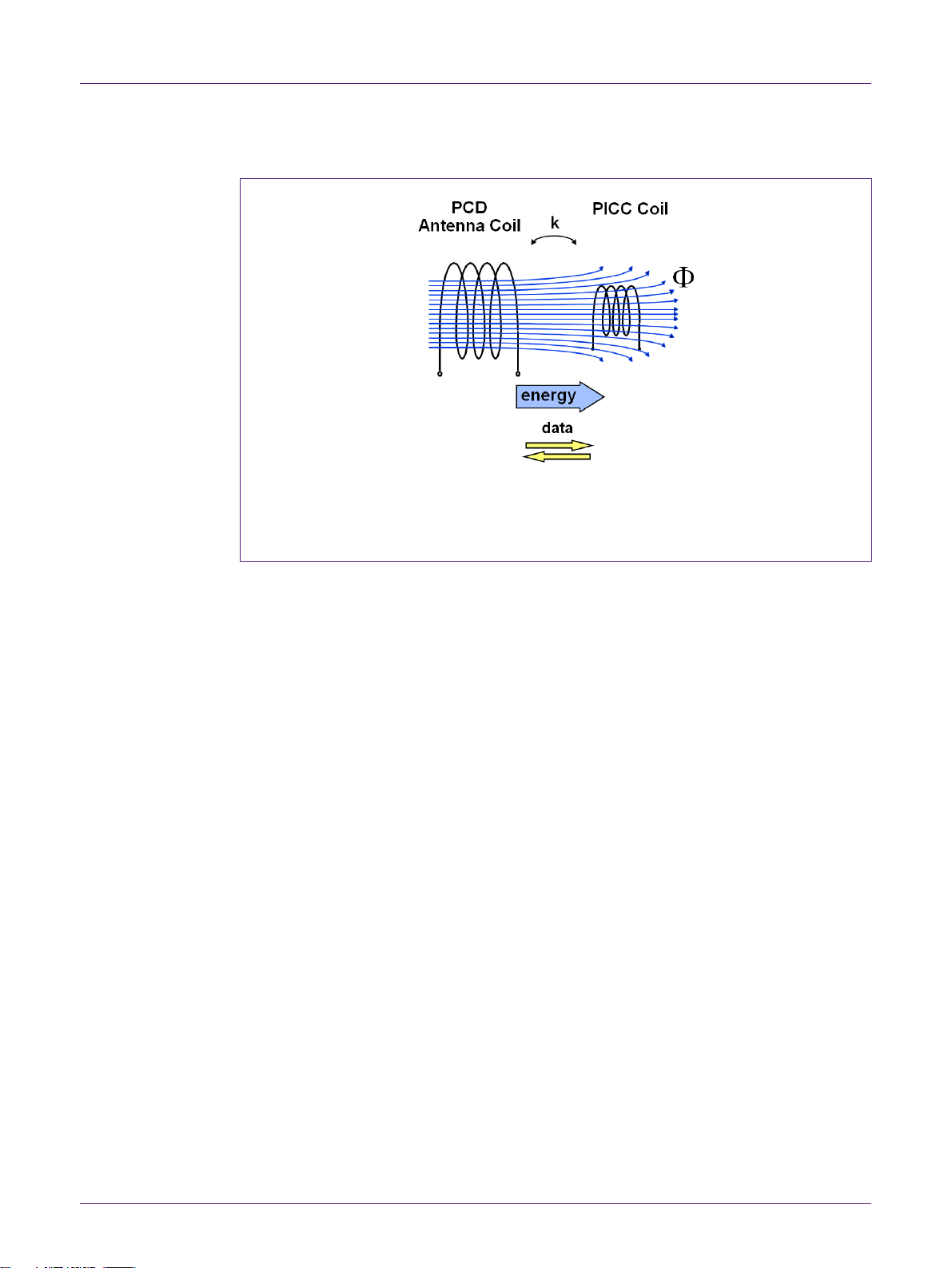
The Fig 1 shows the NFC device in the center, offering all three NFC communication
modes. For the communication between two NFC devices the two different P2P modes
are available:
1. Active P2P: Both NFC devices, the initiator as well as the target, are required to
generate their own magnetic field, when sending data. This mode is optional.
2. Passive P2P: The initiator always generates the magnetic field, while the target
uses the load modulation principle to send its data. This mode is mandatory.
In this document only the analog topics are discussed, which are relevant for the antenna
design. Neither the digital protocol nor the advantages/disadvantages for different use
cases are content of this document.

NXP Semiconductors
AN11740
PN5180 Antenna design
AN11740
All information provided in this document is subject to legal disclaimers.
© NXP B.V. 2018. All rights reserved.
Application note
COMPANY PUBLIC
Rev. 1.1 — 19 June 2018
345311
4 of 62
For the optimization of the performance it might makes sense to restrict the functionality
to only one or two of the communication modes.
(1) ISO/IEC 14443 PICC and PCD here just indicate the similarity of the communication but do not
automatically mean interoperability.
(2) “Extended ISO/IEC14443 PCD/PICC” simply refers to the antenna design parameters and does
not include the protocol.
Fig 1. NFC communication modes
2.1 ISO/IEC 14443 specifics
The ISO/IEC 14443 (called “ISO” in the following, details see [2]) specifies the
contactless interface as widely being used with contactless smartcards.
The ISO/IEC 14443 defines the communication between a reader (“proximity coupling
device” = PCD) and a contactless smartcard (“proximity chip card” = PICC). In four parts
it describes the physical characteristics (i.e. the size of the PICC antennas), the analog
parameters like e.g. modulation and coding schemes, the card activation sequences
(“Anticollision”) and the digital protocol. The ISO/IEC 10373-6 (see [3]) describes the test
setup as well as all the related tests for cards and the reader.
The ISO/IEC 14443 reader antenna consists of an antenna coil, which is matched to the
reader IC. This antenna coil, as shown in Fig 2,
1. generates the magnetic field to provide the power to operate a card (PICC),
2. transmits the data from the reader (PCD) to the card (PICC), and
3. receives the data from the card (PICC) to the reader (PCD).

NXP Semiconductors
AN11740
PN5180 Antenna design
AN11740
All information provided in this document is subject to legal disclaimers.
© NXP B.V. 2018. All rights reserved.
Application note
COMPANY PUBLIC
Rev. 1.1 — 19 June 2018
345311
5 of 62
(1) k = coupling coefficient
(2) Φ = magnetic flux
Fig 2. Magnetic coupling between reader (PCD) and card (PICC)
According to the ISO/IEC 14443 the PICC antenna coils can be categorized into the
classes 1 …6, as shown in Fig 3.
The PCD antenna is not defined as such, but the PCD must support the classes 1, 2, and
3. The support of the classes 4, 5, and 6 is optional.

NXP Semiconductors
AN11740
PN5180 Antenna design
AN11740
All information provided in this document is subject to legal disclaimers.
© NXP B.V. 2018. All rights reserved.
Application note
COMPANY PUBLIC
Rev. 1.1 — 19 June 2018
345311
6 of 62
(1) A PCD must always support the classes 1, 2, and 3. The Classes 4, 5 and 6 are optional.
Fig 3. PICC Classes according to the ISO/IEC 14443
The PCD antenna coil sizes are not specified. So, for ISO/IEC 14443 compliant readers
all different sizes of antenna coils from a few 10 mm2up to 20cm diameter can be found
in various shapes.
The ISO/IEC 14443 does not specify an operating volume. The reader manufacturer
needs to guarantee that within the operating volume - that he himself defines - all related
ISO/IEC 10373-6 tests can be passed.
The compliance tests require calibrated ReferencePICCs, as defined in ISO/IEC10373-6.
The schematic of such ReferencePICC is shown in Fig 4. For each PICC Class there is
one Reference PICC, which needs to be calibrated according to the required
measurement. Practically it makes sense to use one calibrated ReferencePICC for each
measurement case.

NXP Semiconductors
AN11740
PN5180 Antenna design
AN11740
All information provided in this document is subject to legal disclaimers.
© NXP B.V. 2018. All rights reserved.
Application note
COMPANY PUBLIC
Rev. 1.1 — 19 June 2018
345311
7 of 62
(1) Details see [3].
Fig 4. ISO/IEC 10373-6 ReferencePICC
Some ReferencePICCs, which are commercially available (e.g. Fig 5), are pre-calibrated
and equipped with several jumper options to address the most relevant tests with a
single ReferencePICC.
(1) The jumper settings allow the use of different pre-calibration settings.
Fig 5. ISO/IEC 10373-6 Reference PICC Class 1
Still for each PICC Class a separated ReferencePICC is required.
The most relevant analog tests for PCDs are:
1. Field strength test (min and max)
2. Wave shape tests (for all bit rates)
3. Load modulation amplitude tests

NXP Semiconductors
AN11740
PN5180 Antenna design
AN11740
All information provided in this document is subject to legal disclaimers.
© NXP B.V. 2018. All rights reserved.
Application note
COMPANY PUBLIC
Rev. 1.1 — 19 June 2018
345311
8 of 62
Note: This application note does not replace the detailed test description in the ISO/IEC
10373-6.
There is no common certification process for ISO/IEC14443 compliance in place, even
though many national bodies use the ISO/IEC 14443 to operate the electronic passports
and electronic ID cards. For these programs some nations have established a
certification process to guarantee interoperability. An example is given in [5].
2.1.1 Field strength tests
For the field strength test, it is preferred to have the PCD send a continuous carrier, i.e. it
performs no modulation.
The field strength tests simply require the calibrated ReferencePICC and a dc voltage
measurement device (volt meter or oscilloscope). The field strength is equivalent to the
calibrated (and required) voltage level. The ISO/IEC 10373-6 defines minimum voltage
levels, corresponding to the minimum required field strength, and maximum voltage
levels, corresponding to the maximum allowed field strength. The measured voltage
levels must stay in between these limits.
2.1.2 Wave shape tests
The PCD needs to send the related pulse(s): It may send an ISO/IEC 14443 REQA and /
or REQB with the required bit rate, as e.g. specified in [5]. Any other command fits the
purpose, too.
Note: For the test of higher bit rates it makes sense to implement some specific test
commands, which send artificial commands, e.g. REQA and / or REQB, using the coding
and modulation of the corresponding higher bit rates. The standard way of activating
higher bitrates cannot be applied, since the ReferencePICC for ISO/IEC 14443-2 tests
does not allow the protocol layer, which is normally required to switch to higher bit rates.
The wave shape tests require
1. a calibrated ReferencePICC, which is placed at the position of the calibrated field
strength (corresponding to the dc voltage as measured in section 2.1.1),
2. a digital oscilloscope with a measurement bandwidth of 500Msamples or higher, and
3. a tool that filters and transforms the oscilloscope data into the envelope signal
according to the ISO/IEC 10373-6.
The tool normally returns the filtered and transformed envelop as well as the
corresponding values of rise and fall times, residual carrier levels and over- and
undershoots, which must be kept within the given limits.
2.1.3 Load modulation tests
The PCD needs to send a teat command, which allows to check a response from the
ReferencePICC.
The load modulation tests require
1. a calibrated ReferencePICC, which is placed at the position of the calibrated field
strength (corresponding to the dc voltage as measured in section 2.1.1),

NXP Semiconductors
AN11740
PN5180 Antenna design
AN11740
All information provided in this document is subject to legal disclaimers.
© NXP B.V. 2018. All rights reserved.
Application note
COMPANY PUBLIC
Rev. 1.1 — 19 June 2018
345311
9 of 62
2. a signal generator with a pattern generator, that provides the load modulation signal
as a response to the PCD test commands.
The response must be triggered by the PCD test command, i.e. the signal generator
needs a delayed trigger input either from the field or from the PCD itself. The voltage
level of the load modulation input signal for each test case must be (pre-) calibrated in
the TestPCD set up.
The PCD must be able to receive all the responses with the given minimum load
modulation signal level.
2.2 EMVCo specifics
Heading 3 EMVCo specifies a contactless interface for point of sales (POS) terminals (=
PCD) and the corresponding contactless payment cards in [6]. This interface is very
similar to the one defined ISO/IEC 14443, but it uses its own set of requirements and
specification details. The EMVCo test equipment and way of testing is quite different from
the test specification as defined in ISO/IEC 10373-6.
For the reader tests a calibrated EMVCo Reference PICC is required. This Reference
PICC can be bought only from one of the accredited labatories.
Some of the antenna design parameters also need to be adapted towards EMVCo
requirements.
The most relevant analog tests for PCDs are:
1. PCD power test (field strength)
2. Modulation PCD-> PICC tests (wave shape tests)
3. Load modulation tests
EMVCo specifies and requires only the bit rate of 106kbit/s for both type A and B, but no
higher bit rates.
Note: This application note does not replace the detailed test description in the EMVCo
specifcation.
2.2.1 EMVCo Operating volume
One main difference for the tests is the definition of an operating volume, as shown in Fig
6. This volume is tested with the EMV-Reference-PICC.

NXP Semiconductors
AN11740
PN5180 Antenna design
AN11740
All information provided in this document is subject to legal disclaimers.
© NXP B.V. 2018. All rights reserved.
Application note
COMPANY PUBLIC
Rev. 1.1 — 19 June 2018
345311
10 of 62
(1) Details see [6].
Fig 6. EMVCo POS operating volume requirement
Within this volume the given parameters need to be fulfilled.
2.2.2 EMVCo field strength
For the field strength test, it is preferred to have the PCD send a continuous carrier, i.e. it
performs no modulation.
The voltage level which can be measured in all of the given positions needs to be
between the minimum and maximum limit, as given in [6].
Due to the operating volume it can become challenging to meet the EMVCo
requirements with small antennas.
The Fig 7 shows the required power versus antenna size. The curve is based on a
antenna simulation, which uses a few simplifications, so it does not take the loading
effect of the EMVCo Reference PICC into account. On the other the simulation was done
under ideal environmental conditions, i.e. no metal environment influences the antenna.
The simulation results can be taken as reference to estimate the design effort especially
for small antennas compared to “normal” antenna sizes.

NXP Semiconductors
AN11740
PN5180 Antenna design
AN11740
All information provided in this document is subject to legal disclaimers.
© NXP B.V. 2018. All rights reserved.
Application note
COMPANY PUBLIC
Rev. 1.1 — 19 June 2018
345311
11 of 62
(1) Side length of a square antenna.
(2) These simulation results do neither take any specific environment nor loading effects into account.
Fig 7. EMVCo POS Reader antenna size
2.2.3 EMVCo Wave shapes
The PCD needs to send the related pulse(s): It may send an EMVCo REQA and / or
REQB.
The wave shape tests require
3. a calibrated EMVCo ReferencePICC, which is placed at each of the given position
(see Fig 6),
4. a digital oscilloscope with a measurement bandwidth of 500Msamples or higher, and
5. a tool that filters and transforms the oscilloscope data into the envelope signal
according to the EMVCo test requirement.
The tool normally returns the filtered and transformed envelop as well as the
corresponding values of rise and fall times, residual carrier levels and over- and
undershoots, which must be kept within the given limits.
2.2.4 EMVCo Load modulation
The PCD needs to send a test command, which allows to check a response from the
ReferencePICC. Typically, the EMVCo loop back command sequence is used for this.
Note: Since these tests do not replace the certification tests as required by EMVCo,
simple tests commands might be even more useful than the full EMVCo test sequence.
Such a simple test command can be easily debugged and typically allows an easier
triggering.

NXP Semiconductors
AN11740
PN5180 Antenna design
AN11740
All information provided in this document is subject to legal disclaimers.
© NXP B.V. 2018. All rights reserved.
Application note
COMPANY PUBLIC
Rev. 1.1 — 19 June 2018
345311
12 of 62
The load modulation tests require
6. a calibrated ReferencePICC, which is placed at each of the given position (see Fig
6),
7. a signal generator with a pattern generator, that provides the load modulation signal
as a response to the PCD test commands.
The response must be triggered by the PCD test command, i.e. the signal generator
needs a delayed trigger input either from the field or from the PCD itself. The voltage
level of the load modulation input signal for each test case must be set according to [6].
The PCD must be able to receive all the responses with the given minimum load
modulation signal level.
2.3 The NFC specifics
The standard NFC device needs to fulfill the reader mode (PCD), the passive target and
the passive initiator. The passive target from an antenna point of view is very similar to
the optional card mode (PICC).
2.3.1 NFC Operating volume
The NFC Forum specifies an operating volume as shown in Fig 8. All specified
parameters are tested at given test points within this volume. This is valid not only for
reader mode tests, but all tests.
(1) Details see NFC Analog Technical Specification, [4]
Fig 8. NFC Forum operating volume

NXP Semiconductors
AN11740
PN5180 Antenna design
AN11740
All information provided in this document is subject to legal disclaimers.
© NXP B.V. 2018. All rights reserved.
Application note
COMPANY PUBLIC
Rev. 1.1 — 19 June 2018
345311
13 of 62
3. Generic PCD antenna design rules
Some of the antenna and analog design rules are very common for NXP NFC Reader
designs, i.e. they do neither specifically depend on the used standard (ISO, NFC or
EMVCo) nor depend on the NXP Reader IC but rather on physical or technical basics.
3.1 Optimum Antenna Coil
The optimum antenna coil size for a standard PCD can be derived from the Biot-Savart
law. The major prerequisites are some simplifications like the assumption that the
antenna system is optimized based on the parallel operation of smart cards on top of the
PCD antenna. The optimization is derived for the operating distance, i.e. the target is to
show the optimum PCD antenna size for a given required operating distance.
The principle and simplified electrical circuit is shown in Fig 9.
(1) Index 1: PCD
(2) Index 2: PICC
Fig 9. PCD & PICC Antenna coil system
The index 2 indicates the parameters of the PICC. Here the PICC is taken as given, i.e.
the parameters with the index 2 cannot be modified. This is another simplification, but
also refers to the reality, where the reader antenna optimization does not allow to change
card parameters.
The PCD antenna is taken as a circular antenna to allow a simple calculation. The impact
of different form factors is discussed later.
Out of this law the coupling coefficient kbetween PCD and PICC antenna can be
described as following:

NXP Semiconductors
AN11740
PN5180 Antenna design
AN11740
All information provided in this document is subject to legal disclaimers.
© NXP B.V. 2018. All rights reserved.
Application note
COMPANY PUBLIC
Rev. 1.1 — 19 June 2018
345311
14 of 62
A2= Card antenna coil area, fixed
L02 = Card antenna coil single turn inductance, fixed
L01 = Reader coil single turn inductance
r= Reader Antenna coil radius
x= Operating distance in the center of the Reader antenna
µ0= relative permeability
The single turn inductance can be described like this:
d= coil wire diameter with d << r
Note:The formula to calculate the inductance of the antenna coil can only be taken as
reference. In real life many details influence the result, which are not taken into
account in this simple formula. So a measurement of the coil parameters as
described below is required anyway.
3.1.1 Number of turns
Changing the number of turns does not change the coupling, since the inductance itself
has no influence on the coupling. So, in principle antenna coils with a single turn can be
used as well as antenna coils with many turns.
The only remaining parameter to optimize the coupling is the antenna radius r (i.e. the
antenna size), and will be discussed in section 3.1.2.
However, the number of turns changes the inductance which on one hand changes the
matching circuit.
Out of experience it turns out to be optimum to have an inductance around L ≈1µH for a
proper matching, but a wide range of L ≈300nH up to L≈4µH still can be matched
properly, so typically 1 up to 4 turns in the normal range of antenna sizes are used.
The Fig 10 shows the typical inductance values versus the antenna coil radius for 1, 2, 3
and 4 turns. These values are just examples, since the environment, the track width or
wire thickness and some other parameters may influence the inductance.
Furthermore, the typical PCD antenna coil does not use the circular shape, but rather a
rectangular form factor. The given calculated values show the wide range that can be
used, and shall be used as reference only. The antenna coil inductance must be
measured anyway later on to do the antenna matching.
02
01
2
2
3
2
2
2
0
)
(2 L
LA
x
r
r
k⋅
⋅
+
⋅
=
µ
(1)
[ ]
)
2
ln(2
102
7
01
dr
r
m
L⋅
⋅⋅⋅
⋅
≈
−
π
π
(2)

NXP Semiconductors
AN11740
PN5180 Antenna design
AN11740
All information provided in this document is subject to legal disclaimers.
© NXP B.V. 2018. All rights reserved.
Application note
COMPANY PUBLIC
Rev. 1.1 — 19 June 2018
345311
15 of 62
(1) Green area: target area for standard antenna matching.
Fig 10. Inductance examples versus coil radius
On the other hand, the number of turns defines the relationship of voltage level versus
current level. Especially for the load modulation (see Fig 11) it might be helpful to
increase the number of turns on the PCD antenna coil.
(1) Index1 = PCD
(2) Index 2 = PICC antenna coil
Fig 11. Load modulation

NXP Semiconductors
AN11740
PN5180 Antenna design
AN11740
All information provided in this document is subject to legal disclaimers.
© NXP B.V. 2018. All rights reserved.
Application note
COMPANY PUBLIC
Rev. 1.1 — 19 June 2018
345311
16 of 62
3.1.2 Optimum Antenna Coil size
Fig 12 shows the coupling coefficient versus antenna radius for three different operating
distances. The scaling of the coupling coefficient does not necessarily show the correct
absolute value, since some of the fixed parameters are estimated only for this graph.
However, the relative value is important to indicate the optimum antenna size.
(1) Green: at a distance of x = 4 cm
(2) Blue: at a distance of x = 6 cm
(3) Black: at a distance of x = 8 cm
(4) The coupling coefficient scaling in this diagram is relative only. The absolute value might differ.
Fig 12. Coupling coefficient vs PCD antenna radius
The maximum coupling can be achieved, when
r= Reader Antenna coil radius
x= Operating distance in the center of the Reader antenna
The maximum coupling at an operating distance of 4cm can be achieved with an antenna
coil of approximately 4cm radius (i.e. 8cm diameter). Increasing the antenna radius from
4cm to 8cm decreases the coupling at 4cm distance (green curve), but increases the
coupling at 8cm distance (black curve).
However, the optimum antenna size as such does not guarantee that the coupling is
strong enough.
xr =
(3)

NXP Semiconductors
AN11740
PN5180 Antenna design
AN11740
All information provided in this document is subject to legal disclaimers.
© NXP B.V. 2018. All rights reserved.
Application note
COMPANY PUBLIC
Rev. 1.1 — 19 June 2018
345311
17 of 62
The maximum coupling coefficient versus the operating distance can be estimated as
shown in Fig 13. This maximum coupling is related to the optimum antenna size.
(1) The absolute scale of k might not be correct due to simplifications.
Fig 13. Maximum coupling vs antenna size
Theoretical example:
The Fig 14 shows the field strength versus operating distance of two different antenna
sizes. For both antennas the antenna current is tuned to deliver the maximum allowed
field strength of 7.5 A/m at the minimum operating distance of 2mm.
The small antenna with 4cm diameter achieves an operating distance of almost 3cm, the
large antenna with 10cm diameter achieves an operating distance of almost 7cm.

NXP Semiconductors
AN11740
PN5180 Antenna design
AN11740
All information provided in this document is subject to legal disclaimers.
© NXP B.V. 2018. All rights reserved.
Application note
COMPANY PUBLIC
Rev. 1.1 — 19 June 2018
345311
18 of 62
(1) Minimum required field strength Hmin = 1.5A/m
(2) Both antennas scaled to deliver Hmax = 7.5 A/m at maximum
Fig 14. Operating distance x versus antenna size
Note: The large antenna is driven with a current Ilargeantenna ≈4x Ismallantenna.
Note: This graph does not include the detuning and loading effect of the reader
antenna.
The Fig 15 shows the simulation result of three different square antennas. The
magnitude of the field strength is shown versus the distance from the center of the
antenna area in either X or Y direction. The curves indicate the zero points, which are
areas around the antenna slightly outside the antenna area, where no field can be
measured (i.e. where the coupling is zero).
At a zero point no tag device can be operated, even if the required field strength is very
low. This needs to be considered, if there is a requirement to read tags within a certain
given operating volume, which might touch the zero points, especially if the antenna is
too small.

NXP Semiconductors
AN11740
PN5180 Antenna design
AN11740
All information provided in this document is subject to legal disclaimers.
© NXP B.V. 2018. All rights reserved.
Application note
COMPANY PUBLIC
Rev. 1.1 — 19 June 2018
345311
19 of 62
(1) Operating distance = 1cm, X and Y = horizontal distance from antenna center.
(2) These simulation results do neither take any specific environment nor loading effects into account
Fig 15. Magnitude of field strength in 1 cm distance
Note: The field strength is not the same for all three antennas, but has been adjusted
individually to achieve the maximum allowed field strength for each antenna.
3.2 Layout recommendations
The connection between the TX output pins (TX1 and TX2) and the EMC low pass filter
has to be as short as possible. The GND connection especially between TVSS and the
C0A and C0B (see Fig 18) capacitors must be as short as possible.
The connection between the block capacitors and the VDD pins need to be as short as
possible. This holds especially for the TVDD and its block capacitor.
The PN5180 evaluation board and its related description (see [9]) can be taken as a
reference.
The Fig 16 and Fig 17 show a part of the top and bottom layer structure around the
PN5180 as reference. The GND layer is a complete area of one of the middle layers (not
shown).

NXP Semiconductors
AN11740
PN5180 Antenna design
AN11740
All information provided in this document is subject to legal disclaimers.
© NXP B.V. 2018. All rights reserved.
Application note
COMPANY PUBLIC
Rev. 1.1 — 19 June 2018
345311
20 of 62
(1) Part of the top layer
(2) Middle Layer = GND area
Fig 16. PN5180 Layout Reference Board Top layer
Other manuals for PN5180
1
Table of contents
Other NXP Semiconductors Antenna manuals
Popular Antenna manuals by other brands

Wildlife Materials
Wildlife Materials QUICK-CONNECT 3 ELEMENT quick start guide

NKE
NKE HIGH FREQUENCY GPS user manual

Pacific Antenna
Pacific Antenna PAC-12 Assembly instruction

ADRF
ADRF ADXV-HPR user manual

Ubiquiti
Ubiquiti AM-5AC21-60 quick start guide

CommScope
CommScope CMAX-O-CPUSEWV53 Installation instruction