7
freescale.comQuick Start Guide
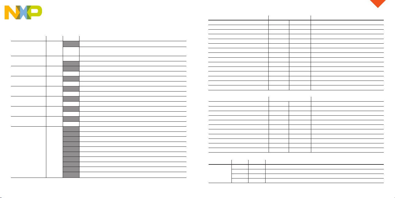
TWR-KM34Z50M Jumper Options
The following is a list of all the jumper options. The default installed jumper settings are
indicated in the shaded boxes.
6
Option Jumper Setting Description
MCU Power
Connection J1
1-2 Connect VBAT to onboard 3.3 V supply
2-3 Connect VBAT to the higher voltage between MCU supply (MCU_PWR)
or VBATD
VREF Out Selection J2 ON VREF connected to ELEVATOR edge
OFF VREF available on pins
MCU_PWR Selection J6 ON MCU powered from V_BRD 3.3 V on board reg.
OFF MCU can be supplied by ext. Voltage connected to J6–pin 1
Analog Power
Enable J7 ON Connect analog voltages to MCU_PWR
OFF Connect analog voltages to MCU_PWR. external VDDA can be applied
Pot. Enable
(might be hardwired) J8 ON Connect PTG1/AD10 to pot. R20
OFF Disconnect PTG1/AD10 from pot. R20
Temp. Sensor Enable
(might be hardwired) J9 ON Connect PTF0/AD7 to temperature sensor
OFF Disconnect PTF0/AD7 to temperature sensor
Low-Power Current
Measurement J19 ON Low-power current measurement bypassed
OFF Low-power current measurement enabled
OpenSDA Reset
Enabled J20 ON KM34 reset input driven by K20 OpenSDA
OFF KM34 reset input isolated from OpenSDA
DIP Switch S1
Connections S1
ON Connect PTE5 to green LED (D3)
ON Connect PTF1 to red LED (D4)
ON Connect PTD1 to orange LED (D5)
ON Connect PTC1 to yellow LED (D6)
ON Connect IRDA Tx LED (D7) to PTC2
ON Connect IRDA Rx transistor (Q1) to PTC3
ON Connect Serial EEPROM data to I2C0 Data
ON Connect Serial EEPROM clock to I2C0 Clock
ON Connect TILT_ENABLE (MMA8491Q) signal to PTF7
ON Connect VBAT voltage measurement signal to PTF2/AD9
GPIO Header (J10) Signal Connections
MCU Signal J10 Pin MCU Signal
SW3 (Tamper switch) 1 2 SW3 to TAMPER1 (when closed)
SW3 (Tamper switch) 3 4 SW3 to TAMPER2 (when closed)
TILT_XOUT 5 6 TILT_XOUT to TAMPER0
TILT_YOUT 7 8 TILT_YOUT to TAMPER1
TILT_ZOUT 9 10 TILT_ZOUT to TAMPER2
V_BRD 11 12 PTI0/SCI1_RXD
PTI1/SCI1_TXD 13 14 GND
PTE0/I2C0_SDA 15 16 PTD7/I2C0_SCL
PTF6/SPI1_MOSI 17 18 PTF5/SPI1_MISO
PTF4/SPI1_SCK 19 20 PTF3/SPI1_SS
PTA6/AFE_EXT_MOD_IN1 21 22 PTF7/CLKOUT
PTC0/AFE_EXT_MOD_IN2 23 24 PTG0
PTB7/AFE_EXT_CLK_IN 25 26 PTC5/AD0
PTA7/AFE_EXT_CLK_OUT 27 28 PTC6/AD1
VSSA_SAR 29 30 GND
Analog Inputs/Generator Out (J17)
MCU Signal J17 Pin MCU Signal
GEN_OUT0 1 2 EXT_SD_ADP0
GEN_OUT1 3 4 EXT_SD_ADP1
GEN_OUT2 5 6 EXT_SD_ADP2
GEN_OUT3 7 8 EXT_SD_ADP3
GEN_OUT4 9 10 EXT_SAR_AD0
GEN_OUT5 11 12 EXT_SAR_AD1
GEN_OUT6 13 14 EXT_SAR_AD2
VSSA 15 16 EXT_SD_ADM0 (can short to VSSA)
VSSA 17 18 EXT_SD_ADM1
VSSA 19 20 EXT_SD_ADM2
VSSA 21 22 EXT_SD_ADM3
K20 Generator Default Operation (SW5 Settings)
Option Position Setting MCU Signal
DIP SW5
Settings
1 OFF K20 USB communication disabled, K20 in Very Low-Power Stop (VLPS) mode
2 OFF Generator output disabled
1 ON USB communication and KM34 current sensing enabled, green LED ON
2 ON Generator output enabled, amber LED ON