NCP1608BOOSTGEVB
http://onsemi.com
7
Rsense +0.5
3.62 +0.138 W
The current sense resistor is selected as 0.125 Wfor
decreased power dissipation. The resulting maximum
inductor peak current is 4 A. Since the MOSFET continuous
current rating is 7 A (for TC= 100°C as specified in the
manufacturer’s datasheet) and the inductor saturation
current is 4.7 A, the maximum peak inductor current of 4 A
is sufficiently low.
The power dissipated by Rsense is calculated using
Equation 18:
PRsense +IM(RMS) 2@Rsense (eq. 18)
PRsense +1.272@0.125 +0.202 W
5. The output capacitor (Cbulk) rms current is
calculated using Equation 19:
IC(RMS) +2
Ǹ@32 @Pout 2
9@p@Vac @Vout @h2*Iload(RMS) 2
Ǹ(eq. 19)
IC(RMS) +2
Ǹ@32 @1002
9@p@85 @400 @0.922*0.252
Ǹ+0.7 A
The value of Cbulk is calculated in Step 5 to ensure a ripple
voltage that is sufficiently low to not trigger OVP. The value
of Cbulk may need to be increased so that the rms current
does not exceed the ratings of Cbulk.
The voltage rating of Cbulk is required to be greater than
Vout(OVP). Since Vout(OVP) is 421 V, Cbulk is selected to have
a voltage rating of 450 V.
DESIGN STEP 7: Supply VCC Voltage
The typical method to charge the VCC capacitor (CVcc) to
VCC(on) is to connect a resistor between Vin and VCC. The
low startup current consumption of the NCP1608 enables
most of the resistor current to charge CVcc during startup.
The low startup current consumption enables faster startup
times and reduces standby power dissipation. The startup
time (tstartup) is approximated with Equation 20:
tstartup +
CVCC @VCC(on)
2
Ǹ@Vac
Rstart *ICC(startup)
(eq. 20)
Where ICC(startup) = 24 mA (typical).
If CVcc is selected as a 47 mF capacitor and Rstart is
selected as 660 kW, tstartup is equal to:
tstartup +47 m@12
2
Ǹ@85
660 k *24 m
+3.57 s
Once VCC reaches VCC(on), the internal references and
logic of the NCP1608 turn on. The NCP1608 includes an
undervoltage lockout (UVLO) feature that ensures that the
NCP1068 remains enabled unless VCC decreases to less than
VCC(off). This hysteresis ensures sufficient time for another
supply to power VCC.
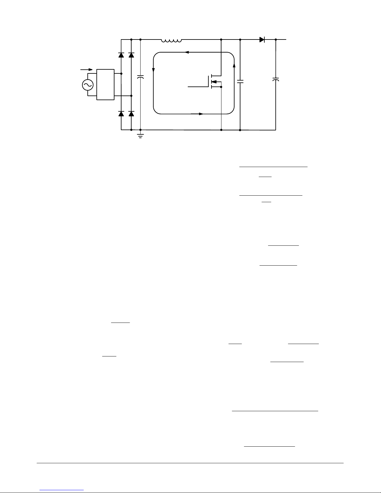
The ZCD winding is a possible solution, but the voltage
induced on the winding may be less than the required
voltage. An alternative is to implement a charge pump to
supply VCC. A schematic is illustrated in Figure 7.
Figure 7. The ZCD Winding Supplies VCC using a
Charge Pump Circuit
+
1
4
3
2
8
5
6
7
GND
ZCD
NCP1608
+
Cin
Rstart
D1
R1
CVcc
RZCD
C3IAUX
DAUX
DRV
VCC
FB
Control
Ct
CS
C3 stores the energy for the charge pump. R1 limits the
current by reducing the rate of voltage change. DAUX supplies
current to C3 when its cathode is negative. When its cathode
is positive it limits the maximum voltage applied to VCC.
The voltage change across C3 over one period is
calculated using Equation 21:
DVC3 +Vout
N*VCC (eq. 21)
The current that charges CVcc is calculated using
Equation 22:
IAUX +C3 @fSW @DVC3 +C3 @fSW @ǒVout
N*VCCǓ
(eq. 22)
For off−line ac-dc applications that require PFC, a 2-stage
approach is typically used. The first stage is the CrM boost
PFC. This supplies the 2nd stage, which is traditionally an
isolated flyback or forward converter. This solution is
cost−effective and exhibits excellent performance. During
low output power conditions the PFC stage is not required
and reduces efficiency. Advanced controllers, such as the
NCP1230 and NCP1381 detect the low output power
condition and shut down the PFC stage by removing
PFC(VCC) (Figure 8).