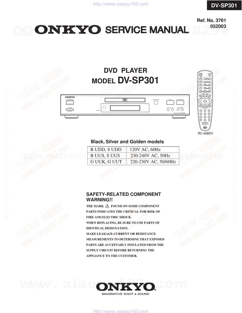
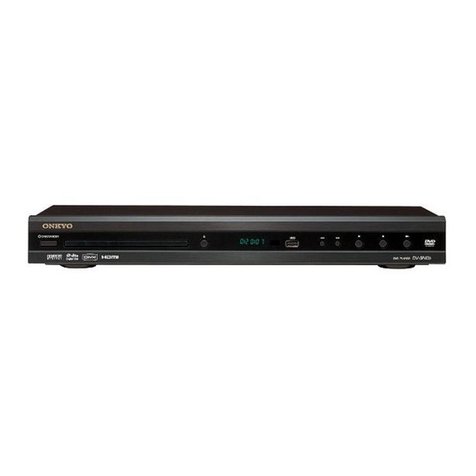
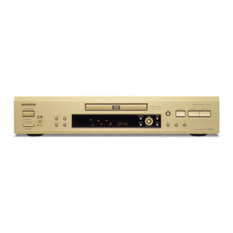
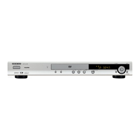
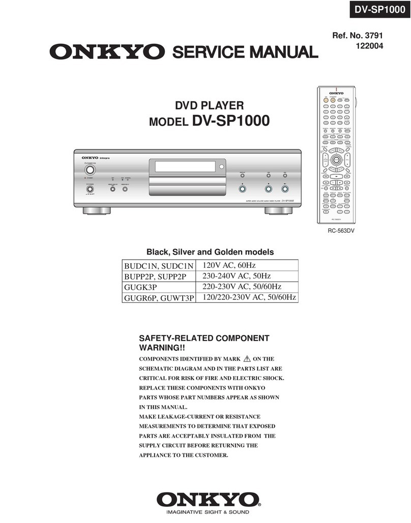
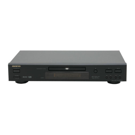
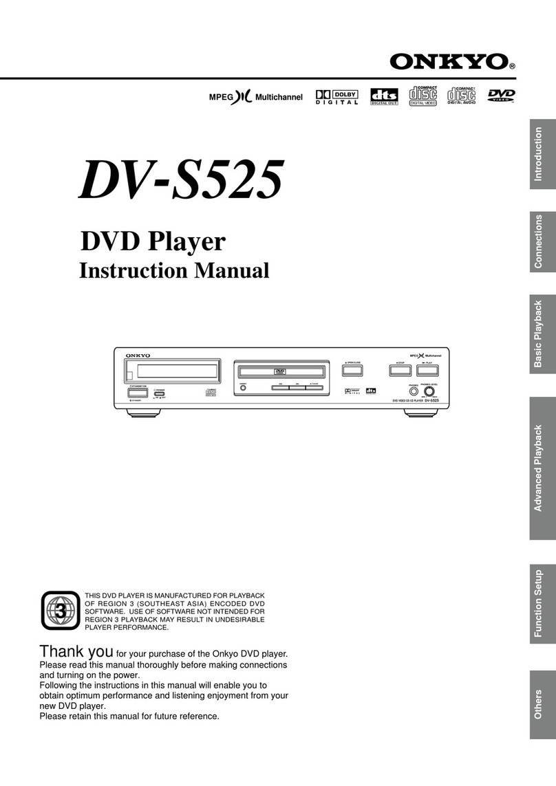
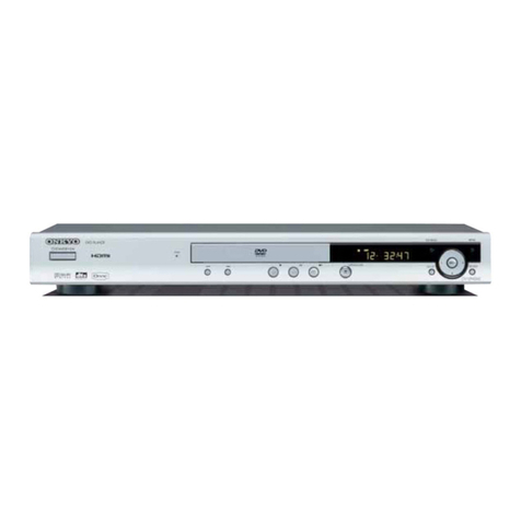
Onkyo DV-S353 User manual

Ref. No.3693
SAFETY-RELATED COMPONENT
WARNING!!
COMPONENTS IDENTIFIED BY MARK ON THE
SCHEMATIC DIAGRAM AND IN THE PARTS LIST ARE
CRITICAL FOR RISK OF FIRE AND ELECTRIC SHOCK.
REPLACE THESE COMPONENTS WITH ONKYO
PARTS WHOSE PART NUMBERS APPEAR AS SHOWN
IN THIS MANUAL.
MAKE LEAKAGE-CURRENT OR RESISTANCE
MEASUREMENTS TO DETERMINE THAT EXPOSED
PARTS ARE ACCEPTABLY INSULATED FROM THE
SUPPLY CIRCUIT BEFORE RETURNING THE
APPLIANCE TO THE CUSTOMER.
072001
SERVICE MANUAL
SERVICE MANUAL
DV-S353
DVD Player
DV-S353
UDD 120V AC, 60Hz
Black model
RC-458DV

DV-S353
Specifications and features are subject to change without notice.
DVD Player
Power supply AC 120 V, 60 Hz
Power consumption 16 W
Weight 8.2 lbs
External dimensions 17 1/8" x 3 7/8" x 12 11/16" (W/H/D)
Signal system NTSC
Frequency range (digital audio) DVD linear sound: 48 kHz sampling 4 Hz to 22 kHz
96 kHz sampling 4 Hz to 44 kHz
Signal-to-noise ratio (digital audio) More than 95 dB
Audio dynamic range (digital audio) More than 95 dB
Harmonic distortion (digital audio) Less than 0.005 %
Wow and flutter Below measurable level
Operating conditions Temperature: 5˚C to 35˚C (41˚F to 95˚F), Operation status: Horizontal
Outputs
Video output 1.0 V (p-p), 75ohm, negative sync., pin jack ×1
S-video output (Y) 1.0 V (p-p), 75ohm, negative sync., Mini DIN 4-pin×1
(C) 0.286 V (p-p), 75ohm
Component video output (Y) 1.0 V (p-p), 75ohm, negative sync., pin jack ×1
(PB)/(PR) 0.7 V (p-p), 75ohm pin jack ×2
Audio output (digital output Optical) Optical connecter ×1
Audio output (digital output Coaxial) 0.5 V (p-p), 75ohm, pin jack ×1
Audio output (2-Channel Audio) 2.0 V (rms), 320ohm, pin jack (L, R) ×1
Supplied Accessories
Audio/video connection cable 1
Remote controller (RC-458DV) 1
Batteries (size AAA/R3) 2
SPECIFICATION

DV-S353
SERVICE NOTES
WARNING
WARNING:
TO REDUCE THE RISK OF FIRE OR ELECTRIC SHOCK,
DO NOT EXPOSE THIS APPLIANCE TO RAIN OR
MOISTURE.
CAUTION:
TO REDUCE THE RISK OF ELECTRIC SHOCK, DO NOT
REMOVE COVER (OR BACK). NO USER-SERVICEABLE
PARTS INSIDE. REFER SERVICING TO QUALIFIED
SERVICE PERSONNEL.
The lightning flash with arrowhead symbol, within an equilateral
triangle, is intended to alert the user to the presence of uninsulated
ìdangerous voltageî within the productís enclosure that may be of
sufficient magnitude to constitute a risk of electric shock to persons.
The exclamation point within an equilateral triangle is intended to alert
the user to the presence of important operating and maintenance
(servicing) instructions in the literature accompanying the appliance.
WARNING
RISK OF ELECTRIC SHOCK
DO NOT OPEN RISQUE DE CHOC ELECTRIQUE
NE PAS
OUVRIR
AVIS
This unit contains a semiconductor laser system and is classified as a
“CLASS 1 LASER PRODUCT”. So, to use this model properly, read
this Instruction Manual carefully. In case of any trouble, please contact
the store where you purchased the unit.To prevent being exposed to the
laser beam, do not try to open the enclosure.
CAUTION:
VISIBLE LASER RADIATION WHEN OPEN AND INTERLOCK
FAILED OR DEFEATED. DO NOT STARE INTO BEAM.
CAUTION:
THIS PRODUCT UTILIZESA LASER. USE OF CONTROLS OR
ADJUSTMENTS OR PERFORMANCE OF PROCEDURES OTHER
THAN THOSE SPECIFIED HEREIN MAY RESULT IN
HAZARDOUS RADIATION EXPOSURE.
The label on the right is
applied on the rear
panel except for USA
and Canadian models.
1. This unit is a CLASS 1 LASER PRODUCT and employs a laser
inside the cabinet.
2. To prevent the laser from being exposed, do not remove the
cover. Refer servicing to qualified personnel.
“CLASS 1 LASER
PRODUCT”
LASER CAUTION
LASER DIODE
Never look at the laser light beam through the objective lens. The visible laser beam may harm
the human eye. Use an appropriate viewer or TV camera to observe the laser beam.
Any laser diode will be damaged by a large current or pulse. Avoid current surges and
electrostatic discharges. Safety grounding of the human body and all measuring equipment, jigs
and tools is absolutely necessary. The use of a grounding mat on the workbench and floor is
necessary. Even a small electrostatic discharge from the human body may destroy the laser
diode instantaneously or reduce its life time.
The pins of the laser diode may be shorted at the factory by a solder bridge at the FPC for
protection during transportation and storage of the unit. If this is the case, open the short circuit
(accessible from the bottom side of the module) quickly with grounded soldering iron (less than
300ÞC).
The damage of the diode might be indicated by an increase of the laser current.
DV-S353
EXPLODEDVIEW
DVD
Power supply PC board
Output terminal PC board
Main circuit PC board
Displaycircuit PC board
S1
22
S2
21
S2
24
S1
S1
30
S4
32
33
11
S1 19 23
S1
30
S1
60
CC201
S1
10
S4
34
25
31
S3
S5
S5
S5
31
30
31
31
S1
31 30
S1
S1
S4
S3
50 31
S4
27
S1
S1
35
70
U1
U1
U2
U3
U5
26
28
29
CC801
CC802
MSW1
Include the display
PC board ass'y
Include the display
PC board ass'y

DV-S353
REF. NO. PART NO. DESCRIPTION
U1 JE010073001A Output terminal PC board ass'y
U2 JE010069001A Display circuit PC board ass'y
U3 JE010063001A Main circuit PC board ass'
y
U5 J4090010150X Power supply PC board ass'y
10 J65100000100 Cord bushing
11 J85820001100 Spacer, PC board
13 J67300026000 3.5MM, sponge
19 J60550012000 Badge, DVD
20 20370190XX Wire tie
21 J85000034000 Front panel
22 J85510003000 Badge, ONKYO
23 J85600024000 Door tray
24 J85200158000 Button, PLAY
25 J85200160000 Knob, POWER
26 J85200157000 Button, OPEN/CLOSE
27 J85200159000 Button, POWER
28 J85300036000 Clear plate
29 J85400058000 Facet, Standby ind.
30 55125120XX Leg (Rear)
31 55141370XX Rubber, leg
32 J60000005300 Chassis
33 J60100015000 Top cover
34 J60110018000 Rear panel
35 J67200019000 Cover, Sensor
50 J85820004000 Shaft power
60 J43730100100 Power cord
70 10675110XX DVD mechanism ass'y, TVM 502 C
CC201 J4112191201X Flexible Flat cable,19P 120mm 1.25mm
CC801 J4112250901X Flexible Flat cable,25P 90mm 1.25mm
CC802 J4112150601X Flexible Flat cable,15P 60mm 1.25mm
S1 833130088 3TTB+8B, Self tapping screw
S2 55127180XX 3 x 8, Flat head bind screw
S3 55127290XX 3 x 18, Bind screw
S4 838430088 3TTB+8(BC), Self tapping screw
S5 J81000300810 3 x 8, Bind screw
MSW1 J46203000101 Power switch
NOTE:THE COMPONENTS IDENTIFIED BY MARK
ARE CRITICAL FOR RISK OF FIRE AND
ELECTRIC SHOCK. REPLACE ONLYWITH
PART NUMBER SPECIFIED.
PARTS LIST (Exploded view)

DV-S353
BLOCK DIAGRAM
DVD MECHANISM
F/E & MECHA.
POWER SUPPLY
PC BOARD
DISPLAY CIRCUIT PC BOARD
OUTPUT TERMINAL PC BOARD

DV-S353
SCHEMATIC DIAGRAM
To power supply PC board
Standby LED PC board
Search backward
Search forward
RED
Skip backward
Skip forward
PLAY/PAUSE
STOP
OPEN/CLOSE
IC901
IC-CXP82324
From Power supply PC board
Front circuit PC board
FL tube
FL901
To main circuit PC board
Power switch PC board

DV-S353
SCHEMATIC DIAGRAM
From Main PC board to Pick up
M GND
Main circuit PC board
From Pickup to main PC board
From main PC board to front PC board
+8V Motor loading VCC
+5V Digital VCC

DV-S353
IC201
ST15519
JIG
PCM LRCLK
PCM CLK
SPDF
GND
PCM DATAD
PCM BICK
R OUT
G OUT
F RESET
DXX INTERRUPT (IRQ2)
To Output terminal PC board
To CP801 To CP802

DV-S353
SCHEMATIC DIAGRAM
Output terminal PC board
From Main PC board
From Main PC board

DV-S353
PC BOARD CONNECTION DIAGRAM
Out put terminal PC board
+8V (VIDEO & AUDIO)
AGND
-8V (VIDEO & AUDIO)
+12V (SCART)
RESET
+3V5D
DGND
+2V5D
+5VD
+12V (MOTOR)
GND (MOTOR)
+8V (LOADING)
CN805
CN-2.5-12P
CN4
CN-2.5-12P
+8V (VIDEO & AUDIO)
AGND
-8V (VIDEO & AUDIO)
+12V (SCART)
RESET
+3V5D
DGND
+2V5D
+5VD
+12V (MOTOR)
GND (MOTOR)
+8V (LOADING)
MGND
+8V (LOADING)
MGND
+12V (MOTOR)
+2V5D
DGND
+5VD
DGND
+3V3D
+5V6S
A-MUTE
V-MUTE
+5VA
AGND
RESET
FPC-ST-15P CP802
CP204FPC-ST-15P
FPC-ST-29P CP801
B
AGND
G
AGND
R
AGND
Y
AGND
CVBS
AGND
C
AGND
NC
DAC AGND
DAC DGND
PCM1748E CS
PCM1748E CLK
PCM1748E DA
PCMCLK
BCK
PCMOUT
LRCLK
NC
NC
DGND
SPDIF
DGND
CP803
CN205
RESET MAIN
TXD
RXD
TV/AUX
CN902
Main circuit PC board
Front display PC board
NC
DGND
SECTOR START
DATA VALID
DATA (EXT DATA)
BIT CLOCK (EXT BCLK)
DGND
RESET (+3V3 RESET)
DXX INTERRUPT (IRQ2)
12C CLOCK (SCL)
12C DATA (SDATA)
DGND
MOTOR GND
+3V3
+5V
DGND
AGND
+12V DISC MOTOR
+8V TRACK MOTOR
CP201
CN-2.0-19P
CN204
CP2
Mecha. F/E PC board
Power supply PC board
Power switch
MSW-1
CN1
CN2
GND
+FL (AC4V5)
-27V
-FL (AC4V5)
+5VS
CN901
GND
+FL (AC4V5)
-27V
-FL (AC4V5)
+5VS)
MCN1
AC Cord
RESET MAIN
TXD
RXD
TV/AUX
WHT
BLK
CN3
GND
LED
KEYIN1
S 5V
4
3
2
1
1
2
3
4
5
6
CP903
4
3
2
1
Standby LED
PC board
Power switch
PC board
CN201
CP205

DV-S353
PARTS LIST (PRINTED CIRCUIT BOARD)
Main circuit PC board
REF. NO. PART NO. DESCRIPTION
ICs
Display circuit PC board
IC201 55130350NR STi5519 Decoder
REF. NO. PART NO. DESCRIPTION
IC202 20940740NR M24C02-MN6 EEPROM
FL tube
IC301 55156290NR HY57V651620BLTC-8 DRAM
FL901 55151330NR HNV-12SM14
IC301 55156420NR KS641632D DRAM
Remote sensor
IC401 55136720NR M29W800AT-90N1 Flash
RM901 J2411320014X RPM6938524 -38kHz
IC501 55133310NR 74HCU04M1R Inverter
Resonator
ICM21 J2113232001X KA8082 Motor driver
X901 55126140NR 10.0MHZ
Transistors
ICs
Q201,Q202, 2097046092 KTC3875S
IC901 55151320NR CXP82532-187Q,
QM201
Microprocessor
Q220B,Q220G, 5513869056 KTN2907A
IC903 J2112505044X KIA7045P 4.5V, Reset
Q220R
Transistor
QM202 2097048092 KTA1504S Chip
Q904 5505124092 KRC107S NPN
Resonator
LED
X501 55128980NR 27.000MHz 16.5PF HC-49/S
D904 55125510NR LTL-1CHE3
Diodes
Diode
DM201 2041428016 MTZ J 5.6B
D906 J2242510011X RB510V-40 Schottky
DM202 J2221510304X RB441Q-40 Schottky
FIG90,FIG92 J65540001200
DM203,DM204 7043654016 1N4148
Coil
Coils
L901 1403936091 22uH, Chip
L204-L207, 5512667050 FCM2012H-102T04 1kohm
Capacitors
L210
C901 2026783041 47uF,16V+/-20%, 5 x 7
L220B,L220G, 1404175091 2.7uH Chip
C906 2025205041 100uF,6.3V+/-20%, 5 x 7
L220R
C907,C917 2026862041 470uF,6.3V+/-20%, 8 x 9
L501,R415 5512667050 FCM2012H-102T04 1kohm
C909 J3470910970X 1uF,50V+/-20%, 5 x 7
Sockets
Sockets AS
CP201 55124600XX 19P 1.25mm ST GF120-19S-TS
CN901 J4300200104X 6P 300MM
CP202,CP203 55125910XX 1.0mm 15P 00-6232-015-006-800
CN902 J4300200107X 6P 80MM
CP204 55124580XX 15P 1.25mm ST GF120-15S-TS
MCN1 J4300200108X
CP205 55124630XX 25P 1.25mm ST GF120-25S-TS
CN903 J4335300101X 4P 160MM 2.0MM
Plugs
Resistors
CN204 J4420040271X
L905,L906 J3013100320X 10 ohm, 1/5W,Metal oxide
Sockets AS
Switches
CN205 J4335300105X 2P 250MM 2.0mm AGW#26
MSW1 J46203000101 SDDLB14700, Power switch
Connectors
SW901,SW903, J46500500501 SKQNAE, Tact
CN201 55123330XX 2.0mm ST GIL-S-6P-S2T2
SW911-SW913,
Capacitors
SW921-SW923
C204,C206, 2026894030 100uF,10V+/-20%, 5 x 11
Others
C210,C221,
050 J67300026000 3.5MM, sponge
C232,C311,
060 J67300025000 6MM, Sponge for sensor
C406
C220B,C220G, 2025267030 470uF,10V+/-20%, 5 x 11
C220R
C223B,C223G, 2025265030 220uF,16V+/-20%, 8 x 11.5
C223R
C228-C231 2026783030 47uF,16V+/-20%, 5 x 11
C233,C505 2026862030 470uF,6.3V+/-20%,
CM203 2026884030 1uF,50V+/-20%, 5 x 11
CM204 1500213030 10uF,16V+/-20%, 5 x 11
CM205 2026902030 100uF,16V+/-20%

DV-S353
1. Connect the printer cable to your PC printer port and connected with down load jig.
2. Set the PC mode into the DOS mode.
3. Copy the driver program ‘DVD_DOWN.EXE’ and main program ‘353v .bin’ into the
same directory( Ex. DVDDL ) then move into the directory.
(3 numeric means version number )
4. Insert the FFC cable to the CP202 silkscreened ‘DOWN LOAD’ on the main Board.
5.Turn on the product and make sure the LED on the jig will be light.
6. type 'DVD_DOWN 353v .bin' then you will see the message below
file size 1897904
word size 978952
Do you want to program FLASH MEMORY? (y/n).
Then press ‘y’
It’ll takes 2 min to be complete down load.
To check embed program version.
Press ‘FR ‘ and ‘standby-on’ button at the same time.
Then fl display below.
7 : (fixed number means ONKYO )
;VersionNumber
; Compile date.
DVD SOFTWARE DOWNLOAD
Main circuit PC board
CP202
115

DV-S353
IC TERMINAL DESCRIPTION
K4S641632D (SDRAM) VDD
DQ0
VDDQ
DQ1
DQ2
VSSQ
DQ3
DQ4
VDDQ
DQ5
DQ6
VSSQ
DQ7
VDD
LDQM
WE
CAS
RAS
CS
BA0
BA1
A10/AP
A0
A1
A2
A3
VDD
1
2
3
4
5
6
7
8
9
10
11
12
13
14
15
16
17
18
19
20
21
22
23
24
25
26
27
54
53
52
51
50
49
48
47
46
45
44
43
42
41
40
39
38
37
36
35
34
33
32
31
30
29
28
PIN CONFIGURATION (Top view)
VSS
DQ15
VSSQ
DQ14
DQ13
VDDQ
DQ12
DQ11
VSSQ
DQ10
DQ9
VDDQ
DQ8
VSS
N.C/RFU
UDQM
CLK
CKE
N.C
A11
A9
A8
A7
A6
A5
A4
VSS
PIN FUNCTION DESCRIPTION
Pin Name Input Function
CLK System clock Active on the positive going edge to sample all inputs.
CS Chip select Disables or enables device operation by masking or enabling all inputs except
CLK, CKE and L(U)DQM
CKE Clock enable Masks system clock to freeze operation from the next clock cycle.
CKE should be enabled at least one cycle prior to new command.
Disable input buffers for power down in standby.
A0~ A11 Address Row/column addresses are multiplexed on the same pins.
Row address : RA0~ RA11, Column address : CA0~ CA7
BA0~ BA1Bank select address Selects bank to be activated during row address latch time.
Selects bank for read/write during column address latch time.
RAS Row address strobe Latches row addresses on the positive going edge of the CLK with RAS low.
Enables row access & precharge.
CAS Column address strobe Latches column addresses on the positive going edge of the CLK with CAS low.
Enables column access.
WE Write enable Enables write operation and row precharge.
Latches data in starting from CAS, WE active.
L(U)DQM Data input/output mask Makes data output Hi-Z, tSHZ after the clock and masks the output.
Blocks data input when L(U)DQM active.
DQ0~ 15 Data input/output Data inputs/outputs are multiplexed on the same pins.
VDD/VSS Power supply/ground Power and ground for the input buffers and the core logic.
VDDQ/VSSQ Data output power/ground Isolated power supply and ground for the output buffers to provide improved noise
immunity.
N.C/RFU No connection
/reserved for future use This pin is recommended to be left No Connection on the device.

DV-S353
IC TERMINAL DESCRIPTION
STI5519 Microprocessor terminal description
DV-S353 MAIN IC201 STI5519 PIN LIST
PIN NUMBER DESCRIPTIO
N
PIN NAME MAIN FUNCTIO
N
TYPE
1PIOs and communication PIO2
[
5
]
PIO2
[
5
]
I/O
2 PIOs and communication PIO2
[
6
]
PIO2
[
6
]
I/O
3 PIOs and communication PIO2
[
7
]
PIO2
[
7
]
I/O
4 - VDD3_3 3.3V POWER SUPPLY POWER
5 - VSS GROUND POWER
6 PIOs and communication PIO3
[
0
]
PIO3
[
0
]
I/O
7 PIOs and communication PIO3
[
1
]
PIO3
[
1
]
I/O
8 PIOs and communication PIO3
[
2
]
PIO3
[
2
]
I/O
9 PIOs and communication PIO3
[
3
]
PIO3
[
3
]
I/O
10 PIOs and communication PIO3
[
4
]
PIO3
[
4
]
I/O
11 PIOs and communication PIO3
[
5
]
PIO3
[
5
]
I/O
12 PIOs and communication PIO3
[
6
]
PIO3
[
6
]
I/O
13 PIOs and communication PIO3
[
7
]
PIO3
[
7
]
I/O
14 - VDD2_5 2.5V POWER SUPPLY POWER
15 - VSS GROUND POWER
16 Front-end B_DATA I2S DATA I
17 Front-end B_BCLK I2C BIT CLOCK I
18 Front-end B_FLAG I2S ERROR FLAG DVD I
19 Front-end B_SYNC I2S SECTOR/ABS TIME I
20 RESERVED RESERVED - I/O
21 RESERVED RESERVED - I/O
22 RESERVED RESERVED - I/O
23 RESERVED VDD_RGB VDDA_RGB=2.5V POWER 2.5V
24 RESERVED VSS_RGB VSSA_RGB=GND POWER GND
25 Video DAC B_OUT B_OUT O
26 Video DAC G_OUT G_OUT O
27 Video DAC R_OUT R_OUT O
28 Video DAC V_REF_RGB V_REF_DAC_RGB I
29 Video DAC I_REF_RGB I_REF_DAC_RGB I
30 Video DAC VDD_YCC VDDA_YCC=2.5V POWER 2.5V
31 Video DAC VSS_YCC VSSA_YCC=GND POWER GND
32 Video DAC Y_OUT Y_OUT O
33 Video DAC C_OUT C_OUT O
34 Video DAC CV_OUT CV_OUT O
35 Video DAC V_REF_YCC V_REF_DAC_YCC I
36 Video DAC I_REF_YCC I_REF_DAC_YCC I
37 - VDD2_5 2.5V POWER SUPPLY POWER
38 - VSS GROUND POWER
39 PIOs and communication PIO4
[
0
]
PIO4
[
0
]
I/O
40 PIOs and communication PIO4
[
1
]
PIO4
[
1
]
I/O
41 PIOs and communication PIO4
[
2
]
PIO4
[
2
]
I/O
42 PIOs and communication PIO4
[
3
]
PIO4
[
3
]
I/O
43 PIOs and communication PIO4
[
4
]
PIO4
[
4
]
I/O
44 PIOs and communication PIO4
[
5
]
PIO4
[
5
]
I/O
45 PIOs and communication PIO4
[
6
]
PIO4
[
6
]
I/O
46 PIOs and communication PIO4
[
7
]
PIO4
[
7
]
I/O
47 - VDD3_3 3.3V POWER SUPPLY POWER
48 AUDIO_DAC VDD_PCM VDD FRE
Q
SYNTHE=2.5V POWER 2.5V
49 AUDIO_DAC VSS_PCM VSS FRE
Q
SYNTHE=GND POWER GND
50 - VSS GROUND POWER
51 AUDIO_DAC DAC_SCLK OVER SAMPLING CLK O
52 AUDIO_DAC DAC_PCMOUT0 PCM_OUT0 O
53 AUDIO_DAC DAC_PCMOUT1 PCM_OUT1 I/O
54 AUDIO_DAC DAC_PCMOUT2 PCM_OUT2 O
55 AUDIO_DAC DAC_PCMCLK PCM_CLOCK I/O
56 AUDIO_DAC DAC_LRCLK LEFT/RIGHT CLK O
57 AUDIO_DAC SPDIF_OUT SPDIF_OUT O

PIN NUMBER DESCRIPTIO
N
PIN NAME MAIN FUNCTIO
N
TYPE
58 Share memor
y
interface SMI_ADR
[
4
]
ADDRESS BUS SDRAM O
59 Share memor
y
interface SMI_ADR
[
5
]
ADDRESS BUS SDRAM O
60 Share memor
y
interface SMI_ADR
[
6
]
ADDRESS BUS SDRAM O
61 Share memor
y
interface SMI_ADR
[
7
]
ADDRESS BUS SDRAM O
62 Share memor
y
interface SMI_ADR
[
8
]
ADDRESS BUS SDRAM O
63 Share memor
y
interface SMI_ADR
[
9
]
ADDRESS BUS SDRAM O
64 - VDD2_5 2.5V POWER SUPPLY POWER
65 - VSS GROUND POWER
66 Share memor
y
interface SMI_ADR
[
0
]
ADDRESS BUS SDRAM O
67 Share memor
y
interface SMI_ADR
[
1
]
ADDRESS BUS SDRAM O
68 Share memor
y
interface SMI_ADR
[
2
]
ADDRESS BUS SDRAM O
69 Share memor
y
interface SMI_ADR
[
3
]
ADDRESS BUS SDRAM O
70 Share memor
y
interface SMI_ADR
[
10
]
ADDRESS BUS SDRAM O
71 Share memor
y
interface SMI_ADR
[
11
]
ADDRESS BUS SDRAM O
72 Share memor
y
interface SMI_ADR
[
12
]
ADDRESS BUS SDRAM O
73 Share memor
y
interface SMI_ADR[13] ADDRESS BUS SDRAM O
74 Share memor
y
interface SMI_CS
[
0
]
CHIP SELECT BANK0 O
75 Share memor
y
interface SMI_CS
[
1
]
CHIP SELECT BANK1 O
76 Share memor
y
interface SMI_RAS RAS SDRAM O
77 Share memor
y
interface SMI_CAS CAS SDRAM O
78 Share memor
y
interface SMI_WE SDRAM WRITE ENABLE O
79 Share memor
y
interface SMI_D
Q
ML D
Q
MASK EN LOW O
80 Share memor
y
interface SMI_D
Q
MU D
Q
MASK EN UP O
81 - VDD3_3 3.3V POWER SUPPLY POWER
82 Share memor
y
interface SMI_CLKIN SDRAM CLOCK IN O
83 - VSS GROUND POWER
84 Share memor
y
interface SMI_DATA
[
0
]
DATA BUS SDRAM I/O
85 Share memor
y
interface SMI_DATA
[
1
]
DATA BUS SDRAM I/O
86 Share memor
y
interface SMI_DATA
[
2
]
DATA BUS SDRAM I/O
87 Share memor
y
interface SMI_DATA
[
3
]
DATA BUS SDRAM I/O
88 Share memor
y
interface SMI_DATA
[
4
]
DATA BUS SDRAM I/O
89 Share memor
y
interface SMI_DATA
[
5
]
DATA BUS SDRAM I/O
90 Share memor
y
interface SMI_DATA
[
6
]
DATA BUS SDRAM I/O
91 Share memor
y
interface SMI_DATA
[
7
]
DATA BUS SDRAM I/O
92 Share memor
y
interface SMI_DATA
[
8
]
DATA BUS SDRAM I/O
93 Share memor
y
interface SMI_DATA
[
9
]
DATA BUS SDRAM I/O
94 - VDD2_5 2.5V POWER SUPPLY POWER
95 Share memor
y
interface SMI_CLKOUT SDRAM CLOCK OUT O
96 - VSS GROUND POWER
97 Share memor
y
interface SMI_DATA
[
10
]
DATA BUS SDRAM I/O
98 Share memor
y
interface SMI_DATA
[
11
]
DATA BUS SDRAM I/O
99 Share memor
y
interface SMI_DATA
[
12
]
DATA BUS SDRAM I/O
100 Share memor
y
interface SMI_DATA
[
13
]
DATA BUS SDRAM I/O
101 Share memor
y
interface SMI_DATA
[
14
]
DATA BUS SDRAM I/O
102 Share memor
y
interface SMI_DATA
[
15
]
DATA BUS SDRAM I/O
103 RESERVED RESERVED I/O
104 RESERVED RESERVED I/O
105 RESERVED RESERVED I/O
106 RESERVED RESERVED O
107 - VDD3_3 3.3V POWER SUPPLY POWER
108 - VSS GROUND POWER
109 JTAG TRAT4 TEST RESET I
110 JTAG TMS TEST MODE SELECT I
111 JTAG TDO TEAT DATA OUT O
112 JTAG TDI TEST DATA IN I
113 JTAG TC
K
TEST CLOCK I
114 TIMER PWM2 PULSE WITDH MODULA2 I/O
115 TIMER PWM1 PULSE WITDH MODULA1 I/O
116 TIMER PWM0 PULSE WITDH MODULA0 I/O

PIN NUMBER DESCRIPTIO
N
PIN NAME MAIN FUNCTIO
N
TYPE
117 EMI Interface CPU_OE OUTPUT_ENABLE I/O
118 EMI Interface CPU_RAM_CLK SDRAM CLOCK O
119 - VDD2_5 2.5V POWER SUPPLY POWER
120 CLOCK & RESET PIX_CLK 27 MHz main clock I
121 - VSS GROUND POWER
122 CLOCK & RESET VDD_PLL VDD PLL=2.5V POWER 2.5V
123 CLOCK & RESET VSS_PLL GND PLL=GND POWER GND
124 CLOCK & RESET RESET CHIP RESET I
125 INTERRUPT IR
Q
2
[
2
]
IR
Q[
2
](
MD_IR
Q)
I
126 INTERRUPT IR
Q
2
[
1
]
IR
Q[
1
](
ATAPI IR
Q)
I
127 INTERRUPT IR
Q
2
[
0
]
IR
Q[
0
](
SERVO_IR
Q)
I
128 EMI Interface CPU_BE
[
0
]
BYTE0 ENABLE O
129 EMI Interface CPU_BE
[
1
]
BYTE1 ENABLE O
130 EMI Interface CPU_RW READ-NOT WRITE O
131 EMI Interface CPU_WATE WATE STATE I
132 EMI Interface CPU_CE
[
4
]
CHIP SEL.BANK3 O
133 EMI Interface CPU_CE
[
3
]
CHIP SEL.BANK2 O
134 EMI Interface CPU_CE
[
2
]
CHIP SEL.BANK1 O
135 EMI Interface CPU_CE
[
0
]
DARAM_RAS0 O
136 - VDD3_3 3.3V POWER SUPPLY POWER
137 - VSS GROUND POWER
138 EMI Interface CPU_RAS1 DARAM RAS I/O
139 EMI Interface CPU_CAS
[
0
]
DARM CAS0 O
140 EMI Interface CPU_CAS
[
1
]
DRAM O
141 EMI Interface CPU_DATA
[
0
]
DATA
[
0
]
I/O
142 EMI Interface CPU_DATA
[
1
]
DATA
[
1
]
I/O
143 EMI Interface CPU_DATA
[
2
]
DATA
[
2
]
I/O
144 EMI Interface CPU_DATA
[
3
]
DATA
[
3
]
I/O
145 EMI Interface CPU_DATA
[
4
]
DATA
[
4
]
I/O
146 EMI Interface CPU_DATA
[
5
]
DATA
[
5
]
I/O
147 EMI Interface CPU_DATA
[
6
]
DATA
[
6
]
I/O
148 EMI Interface CPU_DATA
[
7
]
DATA
[
7
]
I/O
149 - VDD2_5 2.5V POWER SUPPLY POWER
150 - VSS GROUND POWER
151 EMI Interface CPU_DATA
[
8
]
DATA
[
8
]
I/O
152 EMI Interface CPU_DATA
[
9
]
DATA
[
9
]
I/O
153 EMI Interface CPU_DATA
[
10
]
DATA
[
10
]
I/O
154 EMI Interface CPU_DATA
[
11
]
DATA
[
11
]
I/O
155 EMI Interface CPU_DATA
[
12
]
DATA
[
12
]
I/O
156 EMI Interface CPU_DATA
[
13
]
DATA
[
13
]
I/O
157 EMI Interface CPU_DATA
[
14
]
DATA
[
14
]
I/O
158 EMI Interface CPU_DATA
[
15
]
DATA
[
15
]
I/O
159 - VDD3_3 3.3V POWER SUPPLY POWER
160 - VSS GROUND POWER
161 EMI Interface CPU_ADR
[
1
]
ADR
[
1
]
O
162 EMI Interface CPU_ADR
[
2
]
ADR
[
2
]
O
163 EMI Interface CPU_ADR
[
3
]
ADR
[
3
]
O
164 EMI Interface CPU_ADR
[
4
]
ADR
[
4
]
O
165 EMI Interface CPU_ADR
[
5
]
ADR
[
5
]
O
166 EMI Interface CPU_ADR
[
6
]
ADR
[
6
]
O
167 EMI Interface CPU_ADR
[
7
]
ADR
[
7
]
O
168 EMI Interface CPU_ADR
[
8
]
ADR
[
8
]
O
169 EMI Interface CPU_ADR
[
9
]
ADR
[
9
]
O
170 EMI Interface CPU_ADR
[
10
]
ADR
[
10
]
O
171 - VDD2_5 2.5V POWER SUPPLY POWER
172 - VSS GROUND POWER
173 EMI Interface CPU_ADR
[
11
]
ADR
[
11
]
O
174 EMI Interface CPU_ADR[12] ADR[12] O

PIN NUMBER DESCRIPTIO
N
PIN NAME MAIN FUNCTIO
N
TYPE
175 EMI Interface CPU_ADR
[
13
]
ADR
[
13
]
O
176 EMI Interface CPU_ADR
[
14
]
ADR
[
14
]
O
177 EMI Interface CPU_ADR
[
15
]
ADR
[
15
]
O
178 EMI Interface CPU_ADR
[
16
]
ADR
[
16
]
O
179 EMI Interface CPU_ADR
[
17
]
ADR
[
17
]
O
180 EMI Interface CPU_ADR
[
18
]
ADR
[
18
]
O
181 EMI Interface CPU_ADR
[
19
]
ADR
[
19
]
O
182 EMI Interface CPU_ADR
[
20
]
ADR
[
20
]
O
183 EMI Interface CPU_ADR
[
21
]
ADR
[
21
]
O
184 - VDD3_3 3.3V POWER SUPPLY POWER
185 - VSS GROUND POWER
186 PIOs and communication PIO0
[
0
]
PIO0
[
0
]
I/O
187 PIOs and communication PIO0
[
1
]
PIO0
[
1
]
I/O
188 PIOs and communication PIO0
[
2
]
PIO0
[
2
]
I/O
189 PIOs and communication PIO0
[
3
]
PIO0
[
3
]
I/O
190 PIOs and communication PIO0
[
4
]
PIO0
[
4
]
I/O
191 PIOs and communication PIO0
[
5
]
PIO0
[
5
]
I/O
192 PIOs and communication PIO0
[
6
]
PIO0
[
6
]
I/O
193 PIOs and communication PIO0
[
7
]
PIO0
[
7
]
I/O
194 PIOs and communication PIO1
[
0
]
PIO1
[
0
]
I/O
195 PIOs and communication PIO1
[
1
]
PIO1
[
1
]
I/O
196 PIOs and communication PIO1
[
2
]
PIO1
[
2
]
I/O
197 PIOs and communication PIO1
[
3
]
PIO1
[
3
]
I/O
198 - VDD2_5 2.5V POWER SUPPLY POWER
199 - VSS GROUND POWER
200 PIOs and communication PIO1
[
4
]
PIO1
[
4
]
I/O
201 PIOs and communication PIO1
[
5
]
PIO1
[
5
]
I/O
202 PIOs and communication TRIGGER_IN TRIGGER_IN FOR DCU I/O
203 PIOs and communication TRIGGER_OUT TRIGGER_OUT FOR DCU I/O
204 PIOs and communication PIO2
[
0
]
PIO2
[
0
]
I/O
205 PIOs and communication PIO2
[
1
]
PIO2
[
1
]
I/O
206 PIOs and communication PIO2
[
2
]
PIO2
[
2
]
I/O
207 PIOs and communication PIO2
[
3
]
PIO2
[
3
]
I/O
208 PIOs and communication PIO2[4] PIO2[4] I/O

DV-S353
IC TERMINAL DESCRIPTION
FUNCTIONAL BLOCK DIAGRAM
Samsung Electronics reserves the right to change products or specification without notice.
*
Bank Select
Data Input Register
1M x 16
1M x 16
Sense AMP
Output BufferI/O Control
Column Decoder
Latency & Burst Length
Programming Register
Address Register
Row Buffer
Refresh Counter
Row Decoder Col. Buffer
LRAS
LCBR
LCKE
LRAS LCBR LWE LDQM
CLK CKE CS RAS CAS WE L(U)DQM
LWE
LDQM
DQi
CLK
ADD
LCAS LWCBR
1M x 16
1M x 16
Timing Register

DV-S353
REF. NO. PART NO. DESCRIPTION REF. NO. PART NO. DESCRIPTION
ICs Plugs
IC806 55124000NR KIA7906API, Regulator CP803 55090070XX
IC802 55128990NR BA4560F, Op.amp. CP802 55124580XX
IC801 55156030NR PCM1748KE S, DAC CP801 55124630XX
Remote sensor Terminals
IC805 J2123829001X GP1F32T JK801 J44301000900 RCA 1P
Transistors JK802 J44302000600 RCA 2P, JE020
Q801,Q814 2097046092 KTC3875S JK804 J44303000200 RCA 3P RBG
Q802 2097048092 KTA1504S Chip PNP JK803 J44312000100 RCA+S GNDCAP
Q803L,Q803R 5503943092 DTC323T Chip NPN Wire buss
Q805 5513318092 DTC114YKA NPN L801,L804, 20441240XX Wire buss 7.5mm
Q804L 5513319092 DTA114YKA Chip PNP L808
Q803,Q804, 5513869056 KTN2907A PNP L803,L810, 20441210XX Wire buss 20mm
Q807 L811 20441240XX
Q808,Q809, 5513871092 KTD130 NPN L809 20441180XX Wire buss 10mm
Q810-Q813 Diodes
D804 2049651091 1SS355 Chip
D805 7043654016 1N4148
Coil inductors
L805-L807 J2616227920X LAL02 2.7uH
Capacitors
C807 20252680AM 100uF,10V+/-20%, 10 x 16
C809 1500213030 10uF,16V+/-20%,5 x 11
C857,C864, 2025265030 220uF,16V+/-20%, 8 x 11.5
C869
C824,C860 2025267030 470uF,10V+/-20%,
C866 2025267030
C802,C805, 2026783030 47uF,16V+/-20%, 5 x 11
C811L,C811R,
C816L,C816R,
C819,C820
C836 2026894030 100uF,10V+/-20%, 5 x 11
C825 2026911030 330uF,6.3V+/-20%, 6.3 x 11
Socket AS
CN805 J4300200110X 12P 60MM
Output terminal PC board
Other manuals for DV-S353
1
Table of contents
Other Onkyo DVD Player manuals

Onkyo
Onkyo DV-SP403E User manual

Onkyo
Onkyo DV-SP55 User manual

Onkyo
Onkyo DV-SP303 User manual

Onkyo
Onkyo DV-SP502 User manual

Onkyo
Onkyo DV-L5 User manual

Onkyo
Onkyo DV-SP800 User manual

Onkyo
Onkyo DV-HD805 User manual

Onkyo
Onkyo DV-S717 User manual

Onkyo
Onkyo DV-SP300 User manual

Onkyo
Onkyo DX-HD805 User manual

Onkyo
Onkyo DV SP404 User manual

Onkyo
Onkyo DV-SP503E User manual

Onkyo
Onkyo DV-CP701 User manual

Onkyo
Onkyo DV-S555 User manual

Onkyo
Onkyo DV-SP302 User manual

Onkyo
Onkyo DV-SP303 Mounting instructions

Onkyo
Onkyo DV-S555 User manual

Onkyo
Onkyo DV SP504 User manual

Onkyo
Onkyo DV-HD805 User manual

Onkyo
Onkyo DV-SP800 User manual