OPTi MachOne 82C935 Product guide

912-3000-042
Revision: 1.0
July 15, 1997
OPTi®
MachOne™
82C935
Integrated PCI Audio Processor
Data Book

OPTi Inc.
888 Tasman Drive
Milpitas, CA 95035
Tel: (408) 486-8000
Fax: (408) 486-8001
www.opti.com
Copyright
Copyright © 1997, OPTi Inc. All rights reserved. No part of this publication may be reproduced, transmitted, tran-
scribed, stored in a retrieval system, or translated into any language or computer language, in any form or by any
means, electronic, mechanical, magnetic, optical, chemical, manual, or otherwise, without the prior written permis-
sion of OPTi Incorporated, 888 Tasman Drive, Milpitas, CA 95035.
Disclaimer
OPTi Inc. makes no representations or warranties with respect to the design and documentation herein described
and especially disclaims any implied warranties of merchantability or fitness for any particular purpose. Further,
OPTi Inc. reserves the right to revise the design and associated documentation and to make changes from time to
time in the content without obligation of OPTi Inc. to notify any person of such revisions or changes.
Trademarks
OPTi and OPTi Inc. are registered trademarks of OPTi Incorporated.
All other trademarks and copyrights are the property of their respective holders.

MachOne™
Table of Contents
OPTi®
912-3000-042 Page iii
Revision: 1.0
1.0 Overview ...........................................................................................................................1
2.0 Features ............................................................................................................................ 1
3.0 Signal Definitions.............................................................................................................4
4.0 Functional Description .................................................................................................... 9
4.1 AC-LINK...............................................................................................................................................9
4.2 Serial IRQ.............................................................................................................................................9
4.3 3D Sound Enhancement Processor..................................................................................................9
4.4 16-Bit Type F DMA Playback .............................................................................................................9
4.5 Push Button Volume Control.............................................................................................................9
4.6 16-Bit Codec/Mixer ...........................................................................................................................10
4.6.1 Codec...................................................................................................................................10
4.6.2 Mixer.....................................................................................................................................11
4.7 External Serial EEPROM ..................................................................................................................12
4.8 Serial Audio Interface.......................................................................................................................12
4.8.1 I2S-justified format and its variations....................................................................................12
4.8.2 Sony format..........................................................................................................................12
4.8.3 AT&T PCM codec T7525 compatible 16-bit mono format ....................................................12
4.8.4 Testing I2S format (ZV port) with Audio Precision machine.................................................13
4.8.5 Relevant MC register settings ..............................................................................................13
4.8.6 ZV-Port I2S...........................................................................................................................14
4.8.7 Advanced Precision General Purpose Serial Port................................................................14
4.8.8 TDA1311 Stereo Continuous Calibration .............................................................................15
5.0 Register Set ....................................................................................................................16
5.1 PCI Configuration Registers............................................................................................................19
5.2 Legacy Register................................................................................................................................29
5.2.1 MCBase Register .................................................................................................................29
5.2.2 Extended MC Register .........................................................................................................34
5.2.3 SBBase Register ..................................................................................................................35
5.2.4 WSBase Register.................................................................................................................37
6.0 Electrical Specification.................................................................................................. 44
6.1 Absolute Maximum Ratings.............................................................................................................44

MachOne™
OPTi®
Table of Contents (cont.)
Page iv 912-3000-042
Revision: 1.0
6.2 DC Characteristics: 5.0 Volt (VCC = 5.0V ±5%, TA = 0°C to +70°C)..............................................44
6.3 General Specifications: 5.0 Volt (VCC = 5.0V ±5%, TA = 0°C to +70°C).......................................45
6.4 Pin Specifications - Analog (VCC = 5.0V, 25×C) ............................................................................46
6.5 Volume Setting..................................................................................................................................46
6.6 Analog Characteristics.....................................................................................................................46
6.6.1 Analog Inputs........................................................................................................................47
6.6.2 Analog Outputs (10kW, 25pF)..............................................................................................47
6.6.3 Volume Settings ...................................................................................................................47
6.6.4 Analog-to-Digital Converters ................................................................................................48
6.6.5 Digital-to-Analog Converters ................................................................................................48
7.0 Mechanical Package Outlines....................................................................................... 49

MachOne™
List of Figures
OPTi®
912-3000-042 Page v
Revision: 1.0
Figure 2-1 System Block Diagram....................................................................................................................2
Figure 2-2 Simplified Functional Block Diagram...............................................................................................3
Figure 3-1 128-Pin PQFP/LQFP Pin Diagram ..................................................................................................4
Figure 4-1 Functional Block Diagram..............................................................................................................10
Figure 4-2 Mixer Block Diagram .....................................................................................................................11
Figure 4-3 I2S Format.....................................................................................................................................14
Figure 4-4 General Purpose Serial Port, Timing Relationships ......................................................................15
Figure 4-5 Format of Input Signals .................................................................................................................15
Figure 7-1 128-Pin PQFP/LQFP*....................................................................................................................49

MachOne™
OPTi®
Page vi 912-3000-042
Revision: 1.0
List of Tables
Table 3-1 128-Pin Package Pin Listing - Alphabetical Cross-Reference.........................................................5
Table 3-2 Signal Descriptions..........................................................................................................................6
Table 5-1 Register Map .................................................................................................................................16
Table 5-2 PCI Base Register Group: PCICFG 00h-3Fh................................................................................19
Table 5-3 PCI Extended Mode Register Group: PCICFG 40h-FFh...............................................................23
Table 5-4 MCIdx and MCData Registers.......................................................................................................29
Table 5-5 MC Indirect Registers....................................................................................................................29
Table 5-6 Extended MC Register Group: MCIdx 20h-2Fh.............................................................................34
Table 5-7 SBBase Registers for FM and DAP Applications ..........................................................................36
Table 5-8 WSBase Registers for Windows Sound System Applications.......................................................37
Table 5-9 WSBase Register for Codec/Mixer Applications ...........................................................................38
Table 5-10 Codec Indirect Registers ...............................................................................................................39
Table 5-11 Expanded Mode CIR .....................................................................................................................42
Table 7-1 128-Pin PQFP Variable Dimensions .............................................................................................50
Table 7-2 128-Pin LQFP Variable Dimensions..............................................................................................51

MachOne™
Integrated PCI Audio Processor
OPTi®
912-3000-042 Page 1
Revision: 1.0
The information contained within this document is subject to change without notice. OPTi Inc. reserves the right to make changes in this manual at any time as well as in the products it
describes, at any time without notice or obligation. OPTi Inc. assumes no responsibility for any errors contained within. In no event will OPTi Inc. be liable for any damages, direct, indirect, inci-
dental or consequential resulting from any error, defect, or omission in this specification. OPTi and OPTi Inc. are registered trademarks of OPTi Inc. OPTiFM is a trademark of OPTi Inc. All
other trademarks and copyrights are the property of their respective holders. Copyright © 1997 OPTi Inc.
1.0 Overview
The OPTi MachOne™ is a single chip PCI audio processor
that taps the power and performance of the 132MB/sec PCI
bus without sacrificing essential legacy support for the huge
installed base of Sound Blaster™ compatible applications.
With strict adherence to ISA 1.0 and PCI 2.1 PnP standards,
the MachOne delivers the highest assurance of system and
operating system compatibility. The MachOne is ideal for
desktop, notebook, mobile, and embedded applications
requiring a high level of integration and uncompromising
sound quality.
The MachOne’s PCI bus master interface ensures extremely
low system overhead for audio data transfers, freeing the use
of system memory for downloadable MIDI patchsets or
Microsoft DirectMusic™ samples. By utilizing both 3V and
5V, the MachOne delivers the optimal balance between
power consumption and performance.
Hi-Fidelity
OPTi’s third-generation 16-bit Sigma-Delta codec provides
high quality analog-to-digital and digital-to-analog conver-
sions. The Sigma Delta codec is integrated with a low distor-
tion complex mixer and a 3D stereo expander which
dramatically enhances the audio experience with only stan-
dard speakers. Digital audio output provides support for digi-
tal speakers or external mixers, and a General Purpose I/O
port is provided for external audio controllers.
In addition to the 20 OPTiFM™ voices, the MachOne archi-
tecture provides powerful audio software enhancements,
including wavetable, and 3D positioning acceleration—mak-
ing the MachOne an ideal gaming platform. The Digital Game
Port Timer improves overall system performance by offload-
ing from the CPU.
Expandability
The MachOne is an ideal building block for advanced audio
solutions. The MPU-401 port supports external MIDI devices,
such as keyboards. Two sets of asynchronous I/O ports sup-
port Zoom Video, hardware wavetable, speaker phone, Digi-
tal CD-In, DSP data and more.
Mobile Application
The MachOne supports both ACPI and APM which makes it
an ideal audio solution for mobile applications. The MachOne
supports the industry-standard AC-LINK; an ideal docking
station interface. The small audio footprint of the MachOne
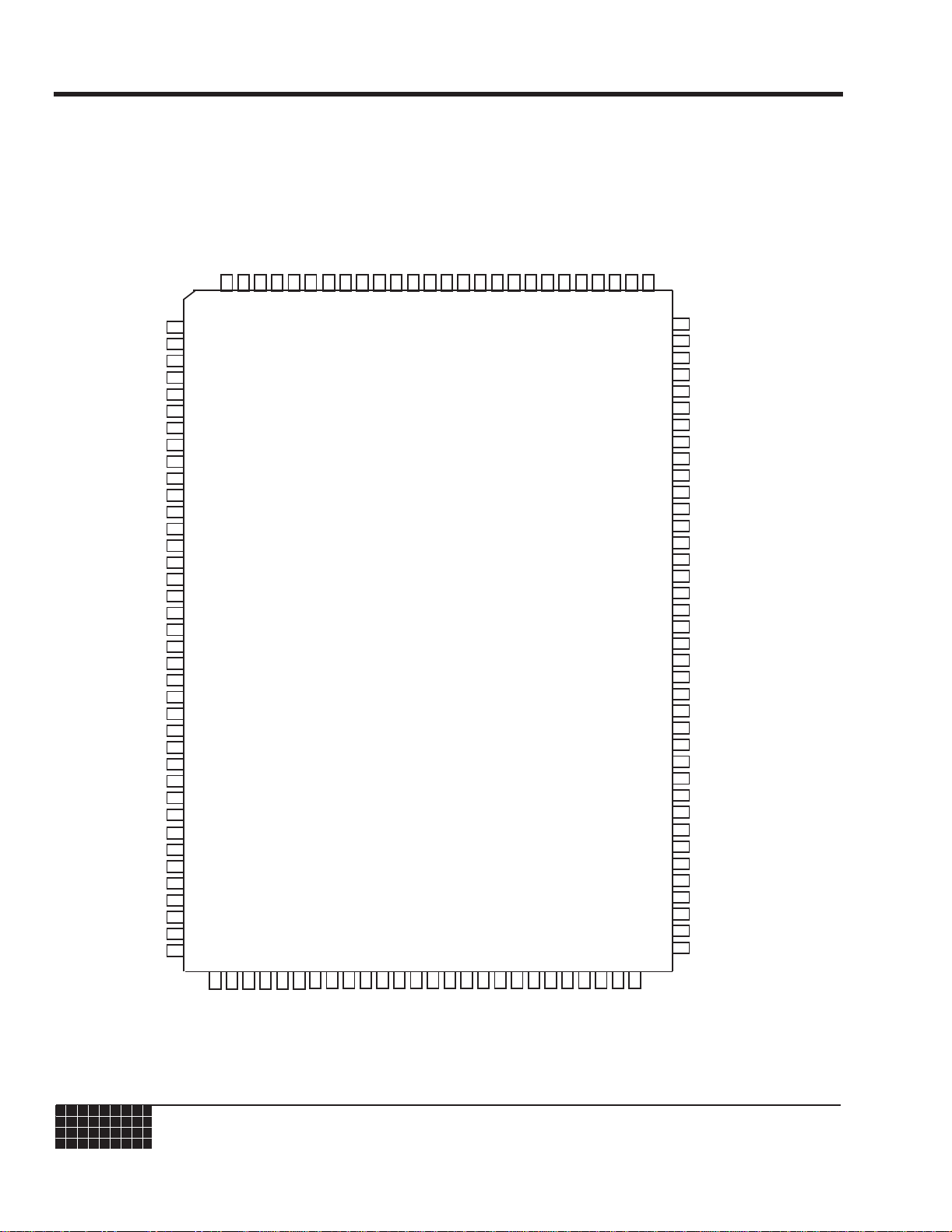
128-pin LQFP package saves valuable real estate which is
prized in space constrained notebook designs.
Integration
The high level of integration of the MachOne eliminates the
requirement for additional memory, codecs, 3D, and other
discrete components. This minimizes the design effort as well
as the total cost of design implementation.
The combination of PCI, outstanding legacy SB Pro Compati-
bility, smallest audio footprint, and Notebook optimization
extensions make the MachOne the ideal audio solution for
desktop, notebook, mobile, and embedded applications
requiring a high level of integration and uncompromising
sound quality.
2.0 Features
• 32-bit PCI Bus Master, PCI 2.1 compliant.
• Integrated sound controller compatible with Sound Blaster
(SB) Pro, Ad Lib, and Microsoft Windows Sound System
(WSS).
• SB Pro/ WSS Compatibility
- Support distributed DMA, virtual DMA with stream scat-
ter/gather buffer control.
- Support Serial IRQ and Drive-back IRQ.
• Support stream scatter/gather buffer to improve PCI bus
bandwidth.
• ISA 1.0 and PCI 2.1 Plug and Play compatible.
• Built-in AC-97 compatible Codec.
• Supports optional external AC-97 Codec through
AC-LINK.
• Full duplex operation: Record and playback simulta-
neously.
• Support IMA ADPCM, µ-Law, A-Law decompression.
• High-quality 20-voice, 52-operator, enhanced OPTiFM
music synthesizer.
• Built-in 16-bit Sigma-Delta Stereo codec.
• Built-in 7-channel mixer: 5 stereo channels and 2 mono
channels.
• 64-step master volume control.
• QSound 3D Sound Enhancement.
• Integrated MIDI UART with FIFO for both input and output
with MPU-401 interface.
• Integrated dual game port with Digital Game Port Inter-
face.

MachOne™
OPTi®
Page 2 912-3000-042
Revision: 1.0
• Push Button Volume Control interface.
• Programmable Serial Port interface for:
- External DSP for sound effect.
- Telephony Codec support.
- External Wave Table digital Interface.
- Zoom Video port.
• Four programmable I/O pins.
• 5V voltage supply.
• Support ACPI power-down mode.
• Digital PC Speaker support.
• 20-bit 1µs resolution DirectX timer.
• 128-pin LQFP package or 128-pin PQFP package.
Figure 2-1 System Block Diagram
82C935
PCI
Line Out
MIDI Port/
Codec/Mixer
Volume Control
Interface
Interface
Line In
CD Audio
AC-97 Codec
AC-97 CODEC I2S ZV Port
Digital Audio I/O
Game Port
Microphone
Volume Up
Volume Down
Mute
Interface
Bus
MachOne

MachOne™
OPTi®
912-3000-042 Page 3
Revision: 1.0
Figure 2-2 Simplified Functional Block Diagram
PCI Bus Digital Audio Processor
MIDI
OPTiFM™
GPIO Register
Serial Audio Interface
PCI Interface
Distributed/Virtual DMA Logic
Interrupt
Game Port Timer/MUX
CODEC/MIXER
Volume Control
UART
CLK
GEN
CONF REGS
Interface
(33MHz)
EEPROM
SIN#
GD[7:0]
AUXL/R
M
IXOUTL/R
MICL/R
CDL/R
LINEL/R
OUTL/R
VOLUP
VOLDWN
49
4
4
RXD
TXD
External
Control
4
AC LINK AC97
Codec
5
Power Management
I2S ZV
Port
3D
Sound
MUTE
Interface
4I2S ZV
Port

MachOne™
OPTi®
Page 4 912-3000-042
Revision: 1.0
3.0 Signal Definitions
Figure 3-1 128-Pin PQFP/LQFP Pin Diagram
1
2
3
4
5
6
7
8
9
10
11
12
13
14
15
16
17
18
19
20
21
22
23
24
25
26
27
28
29
30
102
101
100
99
98
97
96
95
94
93
92
91
90
89
88
87
86
85
84
83
82
81
80
79
78
77
76
75
74
73
GPIO2
AC97-SDI
ROMDI
ROMCLK
ROMD0
ROMCS
GND
AC97-RST#
AC97-SDO
AC97-SYN
AC97-SCLK
SLR2
SCLK2
SDO2
SDI2
VCC
GND
AD0
AD1
AD2
AD3
AD4
AD5
AD6
AD7
CBE0#
GND
AD8
AD9
AD10
122
121
120
119
118
117
116
115
114
113
112
111
110
109
108
107
106
105
104
103
AUXR
VREF1
AVDD
AVSS
AVSS
AVDD
OSCI
OSCO
RXD
TXD
GPIO0
GPIO1
SCLK1
SDI1
SDO1
SLR1
GND
GD0
GD1
GD2
GD3
GD4
GD5
GD6
GD7
VOLUP
VOLDWN
VCC
INTB#
INTC#
45
46
47
48
49
50
51
52
53
54
55
56
57
58
59
60
61
62
63
64
AD25
AD24
IDSEL
CBE3#
GND
AD23
AD22
AD21
AD20
AD19
AD18
AD17
AD16
VCC
CBE2#
FRAME#
IRDY#
TRDY#
DEVSEL#
STOP#
AUXL
OUTR
OUTL
MIXOUTL
CINL
MIXOUTR
CINR
VIDR
VIDL
AVDD
VREF
AVSS
NC
MUTE
NC
NC
NC
NC
NC
GPIO3
82C935
INTA#
SIN#
RST#
GND
CLK
VCC
GNT#
REQ#
AD11
AD12
AD13
AD14
AD15
CBE1#
PAR
GND
CDL
LINEL
MICL
MICR
LINR
CDR128
127
126
125
124
123
31
32
33
34
35
36
37
38
72
71
70
69
68
67
66
65
44
43
42
41
40
39AD31
AD30
AD29
AD28
AD27
AD26
128-Pin Package

MachOne™
OPTi®
912-3000-042 Page 5
Revision: 1.0
Table 3-1 128-Pin Package Pin Listing - Alphabetical Cross-Reference
Signal Name Pin
AC97-RST# 95
AC97-SCLK 92
AC97-SDI 101
AC97-SDO 94
AC97-SYN 93
AD0 85
AD1 84
AD2 83
AD3 82
AD4 81
AD5 80
AD6 79
AD7 78
AD8 75
AD9 74
AD10 73
AD11 72
AD12 71
AD13 70
AD14 69
AD15 68
AD16 57
AD17 56
AD18 55
AD19 54
AD20 53
AD21 52
AD22 51
AD23 50
AD24 46
AD25 45
AD26 44
AD27 43
AD28 42
AD29 41
AD30 40
AD31 39
AUXL 122
AUXR 1
AVDD 3
AVDD 6
AVDD 113
AVSS 4
AVSS 5
AVSS 111
CBE0# 77
CBE1# 67
CBE2# 59
CBE3# 48
CDL 123
CDR 128
CINL 118
CINR 116
CLK 35
DEVSEL# 63
FRAME# 60
GD0 18
GD1 19
GD2 20
GD3 21
GD4 22
GD5 23
GD6 24
GD7 25
GND 17
GND 34
GND 49
Signal Name Pin
GND 65
GND 76
GND 86
GND 96
GNT# 37
GPIO0 11
GPIO1 12
GPIO2 102
GPIO3 103
IDSEL 47
INTA# 31
INTB# 29
INTC# 30
IRDY# 61
LINEL 124
LINER 127
MICL 125
MICR 126
MIXOUTL 119
MIXOUTR 117
MUTE 109
NC 104
NC 105
NC 106
NC 107
NC 108
NC 110
OSCI 7
OSCO 8
OUTL 120
OUTR 121
PAR 66
REQ#‘ 38
ROMCLK 99
Signal Name Pin
ROMCS 97
ROMDI 100
ROMDO 98
RST# 33
RXD 9
SCLK1 13
SCLK2 90
SDI1 14
SDI2 88
SDO1 15
SDO2 89
SIN# 32
SLR1 16
SLR2 91
STOP# 64
TRDY# 62
TXD 10
VIDL 114
VIDR 115
VCC 28
VCC 36
VCC 58
VCC 87
VOLDWN 27
VOLUP 26
VREF 112
VREFI 2
Signal Name Pin

MachOne™
OPTi®
Page 6 912-3000-042
Revision: 1.0
Table 3-2 Signal Descriptions
Signal Name Pin No. Pin Type I/O Type Signal Description To/From
PCI Bus Signals
AD[31:0] 39-46,
50-57,
68-75,
78-85
I/O TTL Address and Data PCI Bus
C/BE#[3:0] 48, 59,
67, 77 I/O TTL-SMT Bus Command and Bus Enable PCI Bus
PAR 66 I/O TTL-SMT Parity PCI Bus
FRAME# 60 I/O TTL-SMT, pull-up Frame, bus cycle start PCI Bus
IRDY# 61 I/O TTL-SMT, pull-up Initiator Ready PCI Bus
TRDY# 62 I/O TTL-SMT, pull-up Target Ready PCI Bus
DEVSEL# 63 I/O TTL-SMT, pull-up Device Select PCI Bus
STOP# 64 I/O TTL-SMT, pull-up Stop cycle PCI Bus
IDSEL 47 I TTL-SMT Initialization Device Select PCI Bus
RST# 33 I TTL-SMT Reset PCI Bus
REQ# 38 O-T TTL Bus Request PCI Bus
GNT# 37 I-T TTL-SMT Bus Grant PCI Bus
INTA#
INTB#
INTC#
31, 29,
30 OD TTL Interrupt Request PCI Bus
CLK 35 I TTL 33MHz Clock PCI Bus
Game Port
GD7 31 I/O CMOS-SMT 8mA Game Port Data Gport/
External
CS
GD6 30
GD5 29
GD4 28
GD3 26 CMOS-SMT 16mA
GD2 25
GD1 24
GD0 23
Serial IRQ
SIN# 32 I/O TTL Serial In/Out
Serial Audio Interface 1
SCLK1 13 I/O TTL Serial Clock SAP
SDI1 14 I TTL Serial Data In SAP
SDO1 15 O TTL Serial Data Out SAP

MachOne™
OPTi®
912-3000-042 Page 7
Revision: 1.0
SLR1 16 O TTL Sample Clock SAP
Serial Audio Interface 2
SCLK2 90 I/O TTL Serial Clock SAP
SDI2 88 I TTL Serial Data In SAP
SDO2 89 O TTL Serial Data Out SAP
SLR2 91 O TTL Sample Clock SAP
EEPROM Interface
ROMCS 97 O TTL ROM Chip Select
ROMCLK 99 O TTL ROM Clock
ROMDO 98 O TTL ROM Data Out
ROMDI 100 I TTL ROM Data In
AC LINK Interface
AC97-RST# 95 O TTL AC97 Reset
AC97-SCLK 92 I TTL AC97 System Clock
AC97-SYN 93 O TTL AC97 SYN
AC97-SDO 94 O TTL AC97 Serial Data Out
AC97-SDI 101 I TTL AC97 Serial Data In
General Purpose Bit I/O
GPIO[3:0] 103,
102, 12,
11
I/O TTL General Purpose Bit I/O
Volume Control
VOLUP 26 I TTL Volume Up
VOLDWN 27 I TTL Volume Down
MUTE 109 I TTL Volume Mute
MIDI Interface Signal
RXD 9 I TTL-SMT Receive Data MIDI Port
TXD 10 O TTL, 20mA Transmit Data MIDI Port
Codec/Mixer Interface Signal
MICL
MICR 125
126 I Analog Microphone Input Left/Right ANALOG
LINEL
LINER 124
127 I Analog Line Input Left/Right ANALOG
CDL
CDR 123
128 I Analog CD Input Left/Right ANALOG
Signal Name Pin No. Pin Type I/O Type Signal Description To/From

MachOne™
OPTi®
Page 8 912-3000-042
Revision: 1.0
AUXL
AUXR 122
1I Analog Auxiliary Input Left/Right ANALOG
VIDL
VIDR 114
115 I Analog Video Input Left/Right ANALOG
OUTL
OUTR 120
121 O Analog
10KΩ, 25pF drive Output Left/Right ANALOG
MIXOUTL
MIXOUTR 119
117 O Analog Mixer Output Left/Right ANALOG
CINL
CINR 118
116 I Analog Analog-Digital Convertor Filter Left/
Right ANALOG
VREFI 2 O Analog Analog Reference ANALOG
VREF 112 O Analog Voltage Reference ANALOG
OSCI 7 I Analog Oscillator Input
OSCO 8 O Analog Oscillator Output
Power, Ground, No Connect (NC) Pins
VCC 28, 36,
58, 87 I PWR Power Connection
GND 17, 34,
49, 65,
76, 86,
96
I GND Ground Connection
AVDD 3, 6, 113 I PWR Analog Power Connections
AVSS 4, 5, 111 I GND Analog Ground Connections
NC 104-108
110 No Connect
Signal Name Pin No. Pin Type I/O Type Signal Description To/From

MachOne™
OPTi®
912-3000-042 Page 9
Revision: 1.0
4.0 Functional Description
The 82C935 is an optimized single chip solution with built-in
Plug-and-Play functions, built-in 3D sound enhancement pro-
cessor, built-in FM synthesizer and 16-bit Sigma-Delta Codec
to provide all of the features needed to create the following
sound characteristics and applications:
• 16-bit sound quality Sound Blaster Pro and Windows
Sound System compatible card
• 3D spatial widened stereo
• 22 voice FM synthesis
• 16-bit CD-quality digital wave audio up to 44.1KHz stereo
• Game port
• MPU-401 MIDI interface
• Wavetable synthesis upgrade
The following sub-sections will discuss these built-in func-
tions in detail.
4.1 AC-LINK
The 82C935 supports an external AC-LINK codec (AC97).
4.2 Serial IRQ
The 82C935 supports serial IRQ. The IRQ signal is transmit-
ted through pin 32. The SIRQ is enabled at bit 0 of PCI
Extended Register PCICFG 62h.
4.3 3D Sound Enhancement Processor
The 82C935 includes the 3D sound enhancement processor
from QSound Labs Inc. The 3D audio enhancement is
achieved while using normal left-and-right channel stereo
speakers.
The following block diagram shows the functional element of
the 3D sound enhance processor in the 82C935.
4.4 16-Bit Type F DMA Playback
The 82C935 supports the Type F DMA playback.
4.5 Push Button Volume Control
In silicon revision 1.0, three pins are used as volume control
push-buttons (pin 27 as volume down, pin 26 as volume up,
and pin 109 as mute) so that the speaker volume can be con-
trolled through front panel buttons in desktop or notebook
PCs. Appropriate software drivers are needed to enable this
feature.
These three pins are active-low, edge-triggering and pulled
up internally. When the button is pressed and the corre-
sponding pin is activated, the register bits MCIR16[5:3] are
set accordingly. The software drivers poll these three bits
periodically. The scheme is as follows:
The register bits MCIR16[5:3] will be cleared automatically
after they are read by the driver.
AC-LINK Type Set 1 (128-Pin)
AC97-RST# O GPIO1 (pin 95)
AC97-SYN O INTC# (pin 93)
AC97-SCLK I SIN# (pin 92)
AC97-SDO O VOLUP (pin 94)
AC97-SDI I VOLDWN (pin 101) Buttons MCIR16[5:3]
(BUTUP:BUTDN) Action required for the
driver
Press UP button 100 increase the volume by
one step
Press Down button 010 decrease the volume by
one step
Press Mute button 001 mute
Spatial
Stereo In
L
R
Stereo
Switch
L
R
Stereo Out
Enhancement
BYP

MachOne™
OPTi®
Page 10 912-3000-042
Revision: 1.0
4.6 16-Bit Codec/Mixer
4.6.1 Codec
Features of the built-in 16-bit stereo sigma-delta codec
include:
• Sigma-delta stereo ADC with 128X over-sampling
• Sigma-delta stereo DAC with 128X over-sampling
• On-chip 8X Interpolation Filter
• On-chip analog post filter
• Single-ended input and output
• Sampling rate of 5KHz to 48KHz
The codec serial interface provides a means to read and
write 16-bit stereo data from the ADC or to the DAC respec-
tively. The interface (as shown in Figure 4-1) consists of the
following lines:
• DAC[15:0] - to write to the DAC 16-bit input
• ADC[15:0] - to read the ADC 16-bit output
• L/R - to select between the left and right channels for both
the ADC and DAC data.
• MCLK - This internal master clock signal is synthesized by
the frequency synthesizer from the crystal reference of
14.318MHz. One of 236 frequencies may be selected
through the 8-bit FSEL line. MCLK is not active when the
frequency synthesizer is powered down. The frequency of
MCLK is 256 times the sampling frequency.
The DAC left/right 16-bit input data are multiplexed onto
DAC[15:0] and fed into the codec. The L/R signal qualifies
the data. The period of L/R is equal to that of the codec sam-
pling frequency. One set of left/right 16-bit input data to the
DAC is sent every L/R cycle. When L/R is low, the data on
DAC[15:0] is meant for the left channel; when L/R is high, the
data is meant for the right channel. This means that the DAC
treats data packets L1 and R1 as belonging to the same sam-
pling instance; while L2 and R2 are data for the next sam-
pling instance.
The ADC left/right 16-bit output data are similarly multiplexed
onto the ADC[15:0] bus.
Figure 4-1 Functional Block Diagram
AVCC
AGND
CINR
CINL
DACL
DACR
VREF
MCLK
Stereo 16-Bit Sigma-Delta ADC
Analog 128:1
1
128fs
16
Analog
fs
16
Stereo 16-Bit Sigma-Delta DAC
Digital
8fs
8X
Voltage Reference
Clock Generation
Power Supply
VCC VCC PD
Sigma-Delta
Modulator Decimation
Filter
Analog
Sigma-Delta
Modulator
128:1
Decimation
Filter
1
128fs
16
fs
Low-Pass
Filter Sigma-Delta
Modulator Interpolator
Analog Digital 8X
Low-Pass
Filter Sigma-Delta
Modulator Interpolator
16
8fs

MachOne™
OPTi®
912-3000-042 Page 11
Revision: 1.0
4.6.2 Mixer
The built-in mixer mixes two mono microphone level inputs
(MICL/R) and five stereo analog line level input sources
(LINEL/R, CDL/R, AUXL/R, FML/R, and DACL/R) with indi-
vidual mixer programmable gain and mute control. The
DACL/R stereo analog inputs are routed to a programmable
circuit with 1.5dB steps (total of 32 levels). Internal amplifiers
with a programmable 20dB gain block are provided for the
MIC input (only). The remaining stereo analog inputs are
routed to a programmable gain circuit which can be pro-
grammed in 3dB steps (total of 16 levels). Also, internal
amplifiers with a programmable 20dB gain block are pro-
vided. Level changes only take effect on zero crossings to
minimize audible artifacts. AC coupling is mandatory for
these inputs since any DC offset on the input will be ampli-
fied.
MIXOUTL (mixer record output left) must be connected to
CINL (codec analog input left) with a ceramic capacitor. MIX-
OUTR (mixer record output right) must be connected to CINR
(codec analog input right) with a ceramic capacitor. MIX-
OUT/R are routed via gain control (1.5dB steps: total of 16
levels). Analog output OUTL/R are routed via a master vol-
ume control which provides 0db to 94.5db of attenuation,
adjustable in 3dB steps. The Codec Indirect Registers used
for programming the various functions/gain levels for the
mixer. For details regarding these registers, refer to Table 5-
10 in the Register Section. Figure 4-2 shows a functional
block diagram of the mixer.
Figure 4-2 Mixer Block Diagram
MICL/R
16 Levels
–33 to 12dB
0 to -93dB
0 to 22.5dB
(1.5dB step)
MIXOUTL/R
OUTL/R
32 Levels
∑
(3dB steps)
LINEL/R
CDL/R
AUXL/R
FML/R
DACL/R
ATTEN
+
MUTE
ATTEN
+
MUTE
ATTEN
+
MUTE
ATTEN
+
MUTE
ATTEN
+
MUTE
ATTEN
+
MUTE
+20dB Mux
Zero
Cross
Detect
Mixer Latch Control
(3dB steps)
0 to –46.5dB
(1.5dB step)
2
2
2
2
2
2
2
2
2
2
2
2
2
2
2
2
2 2
2
22
Gain
(16 Levels)
Master Volume
ATTEN/MUTE
(32 Levels)

MachOne™
OPTi®
Page 12 912-3000-042
Revision: 1.0
4.7 External Serial EEPROM
The 82C935 has the resource data and serial identifier
required by the PnP specification stored internally. If an OEM
customer wants to use a different resource data and serial
identifier to customize their application, an external EEPROM
can be used. To use an external EEPROM, pin 97 (ROMCS)
must be pulled low. This enables the resource data and serial
identifier to be read from the external EEPROM instead of the
82C935’s internal storage.
The 82C935 provides a serial EEPROM interface that is com-
patible with devices from a number of vendors. Pin 99 of the
82C935 provides the data clock for the EEPROM. Pin 98 pro-
vides data to the EEPROM, while pin 100 gets input from the
EEPROM.
4.8 Serial Audio Interface
The 82C935 supports two sets of serial audio interface.
The 82C935's serial audio interface supports the following
formats:
•I
2
S-justified format (ZV port) and its variations.
• Sony format (short right-justified format, used by OPTi's
wavetable chip and the Philips TDA1311AT DAC).
• AT&T PCM codec T7525 compatible16-bit mono format.
Please refer to sections 4.8.6,
ZV-Port I2S
, 4.8.7,
Advanced
Precision General Purpose Serial Port
, 4.8.8,
TDA1311 Ste-
reo Continuous Calibration
, for the respective timing dia-
grams.
4.8.1 I2S-justified format and its variations
In the I2S-justified format (ZV-port), LRCLK is low for the left
channel, and high for the right channel. The left-channel MSB
is left-justified to the high-to-low LRCLK transition with a sin-
gle SCLK delay. SDATA could be SADI when the 935 is in
receive mode, and SADO when the 935 is in transmit mode.
The LRCLK period is programmable with a minimum of 32
SCLKs (MC22[4]). The following example assumes LRCLK
period is greater than 32 SCLKs. Please note that in ZV port,
there is one more signal MCLK defined but this is not needed
for the 935.
To program the 935 in the I2S-justified mode, the MC22 and
MC21 registers need to be set. The relevant MC22 and
MC21 bit definitions are shown below for reference.
I2S-justified mode (ZV-port):
MC22[7:0] = "00110001" (31H).
MC21[7:0] = "10000010" (82H).
There are other I2S variations: left-justified and right-justified.
For the left-justified, LRCLK is high for the left channel, and
low for the right channel. The MSB is left-justified to an
LRCLK transition, with zero SCLK delay.
MC22[7:0] = "00110100" (34H).
MC21[7:0] = "10000010" (82H).
For the right-justified, LRCLK is high for the left channel, and
low for the right channel. The MSB is delayed from an LRCLK
transition, the LSB will be right-justified to the next LRCLK
transition.
MC22[7:0] = "00010100" (14H).
MC21[7:0] = "10000010" (82H).
4.8.2 Sony format1
This data format is essentially the same as the I2S right-justi-
fied format. Normally there are only 32 SCLKs in a LRCLK
period. The LRCLK is high for the left channel, and low for the
right channel. The MSB comes in first. To set up the 935 in
Sony format:
MC22[7:0] = “00000100” (04H).
MC21[7:0] = “10000010” (82H).
4.8.3 AT&T PCM codec T7525 compatible 16-bit
mono format
The 935 supports the T7525 receive timing - word format with
positive FSYNC. The benefit is that the 935's secondary DAC
could be used to save a T7525 as the voice codec in
modem/audio combo solution. To program the 935 in T7525
mode: MC22[7:0] = “00110010” (32H)
MC21[7:0] = “10000010” (82H)
In short summary:
* The MC22[4] bit setting may vary, depending on the LRCLK
period (32 SCLK or more).
1. Short right-justified format, used by OPTi's wavetable chip and the Philips TDA1311AT DAC.
Set 1 Set 2
SCLK Pin 13 Pin 90
SDI Pin 14 Pin 88
SDO Pin 15 Pin 89
SLR Pin 16 Pin 91
I2S-
justified left-
justified right-
justified Sony
format T7525
format
MC22[7:0] 31H* 34H* 14H* 04H* 32H
MC22[7:0] 82H

MachOne™
OPTi®
912-3000-042 Page 13
Revision: 1.0
4.8.4 Testing I2S format (ZV port) with Audio Pre-
cision machine
The Audio Precision machine system two 2322 has a serial
audio data port that can generate a test tone in the I2S format
with programmable FSYNC, ranging from 24KHz to 48KHz.
The 935 was tested with AP machine in various test tones:
256Hz, 1KHz and 3KHz in both sine wave and square wave
with FSYNC = 48KHz.
To test out the feature, the AP machine is hooked up with the
935 with appropriate connections (AP's pin#6, 12, 14 are
SDATA, SCLK and FSYNC, respectively). The next step is to
setup the MC22 to “31H” and MC21 to “82H”. Then the test
tone could be heard from the speaker connected to the 935.
Please note that there might be some noise in the speaker.
This is due to unshielded cable used to connect the serial
audio interface. Shielding the cable would help improve the
audio quality.
4.8.5 Relevant MC register settings
Bit 5 First16-bit: Specifies where the data is located in the LRCLK period
0: data located at the last 16 bits of the left/right channel in an LRCLK period
1: data located at the first 16 (or 17) bit of the left/right channel in an LRCLK period
Bit 4 CLK32: Specifies the number of SCLKs per LRCLK period, used only in delay-mode or pulse-mode ASIO
0: 32 SCLK per LRCLK period
1: more than 32 SCLK per LRCLK period
Bit 3 SCLK polarity:
0: SDATA and LRCLK change at the rising edge of SCLK
1: SDATA and LRCLK change at the falling edge of SCLK
Bit 2 FSYNC (LRCLK) polarity:
0: LRCLK is LOW for the left channel, HIGH for the right channel
1: LRCLK is HIGH for the left channel, LOWfor the right channel
Bit 1 Pulse mode: Used for AT&T T7525 codec or CS8412 DSP data format
0: Pulse mode disabled
1: Pulse mode enabled, used for AT&T T7525 or CS8412 data format
Bit 0 I2S mode: MSB delay mode
0: Zero SCLK delay from an LRCLK transition to MSB data
1: One SCLK delay from an LRCLK transition to MSB data
bit [7:6] CTL_SEL[1:0]: ASIO shift clock selection
00/11: Use the shift clock from internal FS
01: Use FM timing
10: Use external SCLK
bit 1 FDACSEL: selects the data source to the FDAC
0: FDAC takes FM data
1: FDAC takes SADI (if SPCDSEL=0) or second DMA playback data (if SPCDSEL=1)
MC22 Serial Audio format control register (R/W) Default: 00h
bit 7 bit 6 bit 5 bit 4 bit 3 bit 2 bit 1 bit 0
Reset ASIO ASIO test
enable First16-bit CLK32 SCLK
Polarity FSYNC
Polarity Pulse Mode I2S Mode
MC21 Serial Audio selection control register (R/W) Default: 00h
bit 7 bit 6 bit 5 bit 4 bit 3 bit 2 bit 1 bit 0
CTL_SEL[1:0] P2S_SEL[1:0] SPCDSEL ADCSEL FDACSEL DACSEL

MachOne™
OPTi®
Page 14 912-3000-042
Revision: 1.0
4.8.6 ZV-Port I2S
4.8.6.1 LRCLK
This signal determines which audio channel (left/right) is cur-
rently being input on the audio Serial Data input line. LRCLK
is low to indicate the left channel andhigh to indicate the right
channel. Typical frequency values for this signal are 48KHz,
44.1KHz, 32KHz, and 22KHz.
4.8.6.2 SDATA
This signal is the digital PCM signal that carries the audio
information. Digital audio data is transferred using the I2S for-
mat.
I2S Format
The I2S format is shown below. The digital audio data is left
channel-MSB justified to the high-to-low going edge of the
LRCLK plus one SCLK delay.
Figure 4-3 I2S Format
4.8.6.3 SCLK
This signal is the serial digital audio PCM clock.
4.8.6.4 MCLK
This signal is the Master clock for the digital audio. MCLK is
asynchronous to LRCLK, SDATA and SCLK.
The MCLK must be either 256x or 384x the desired Input
Word Rate (IWR). IWR is the frequency at which words for
each channel are input to the DAC and is equal to the LRCLK
frequency. The following table illustrates several standard
audio word rates and the required MCLK and LRCLK fre-
quencies. Typically, most devices operate with 384fx master
clock.
The ZV Port audio DAC should support an MCLK frequency
of 384fs. This results in the frequencies shown below.
4.8.7 Advanced Precision General Purpose
Serial Port
The 15-pin "D-sub" connector on the rear panel provides all
input and output signals for a general purpose serial
input.output port, plus DSP-program specific input and output
pins which may be used in certain DSP (.AZ2) programs. The
pinout of the connector is detailed below. All inputs are TTL
level compatible CMOS. All outputs are CMOS isolated by
50Ωseries resistors and rise time limiting networks.
LRCLK
SCLK
SDATA
Left Channel Right Channel
15141312111098 76543 21015141312111098 76543 210
LRCLK (KHz)
Sample Frequency SCLK (MHz)
32xfs MCLK (MHz)
384x
22 0.704 8.448
32 1.0240 12.2880
44.1 1.4112 16.9344
48 1.5360 18.4320
Pin Function Pin Function
1 Ground 9 Serial Input Master
Clock (input)
2 +5V (tied to unused
inputs high) 10 Serial Input Bit Clock
(input)
3 Auxiliary Input (DSP
program specific) 11 Auxiliary Output (DSP
program specific)
4 Ground 12 Serial Output Bit
Clock (output)
5 Ground 13 Serial Input Data
(input)
6 Serial Output Data
(output) 14 Serial Output Frame
Sync (output)
7 Ground 15 Serial Input Frame
Sync (input)
8 Ground
Table of contents
Popular Computer Hardware manuals by other brands

Fujitsu Siemens Computers
Fujitsu Siemens Computers POCKET LOOX N100 series operating instructions

DAQ system
DAQ system PCIe-FRM13 user manual

Audio Control
Audio Control OVERDRIVE Concert Series owner's manual

National Instruments
National Instruments NI PXI-8221 user manual

Waudio
Waudio SCS 224 user manual

Delta
Delta CMM-DN01 Operation manual