1 SAFETY PRECAUTIONS 3
1.1. GENERAL GUIDELINES 3
2 PREVENTION OF ELECTRO STATIC DISCHARGE (ESD) TO
ELECTROSTATICALLY SENSITIVE (ES) DEVICES 4
3 Precaution of Laser Diode 5
3.1. About lead free solder (PbF) 5
4 General Description 6
4.1. Operating instructions 6
5 PREVENTION OF STATIC ELECTRICITY DISCHARGE 7
5.1. Grounding for electrostatic breakdown prevention 7
5.2. Handling Precautions for Traverse Unit (Optical Pickup) 7
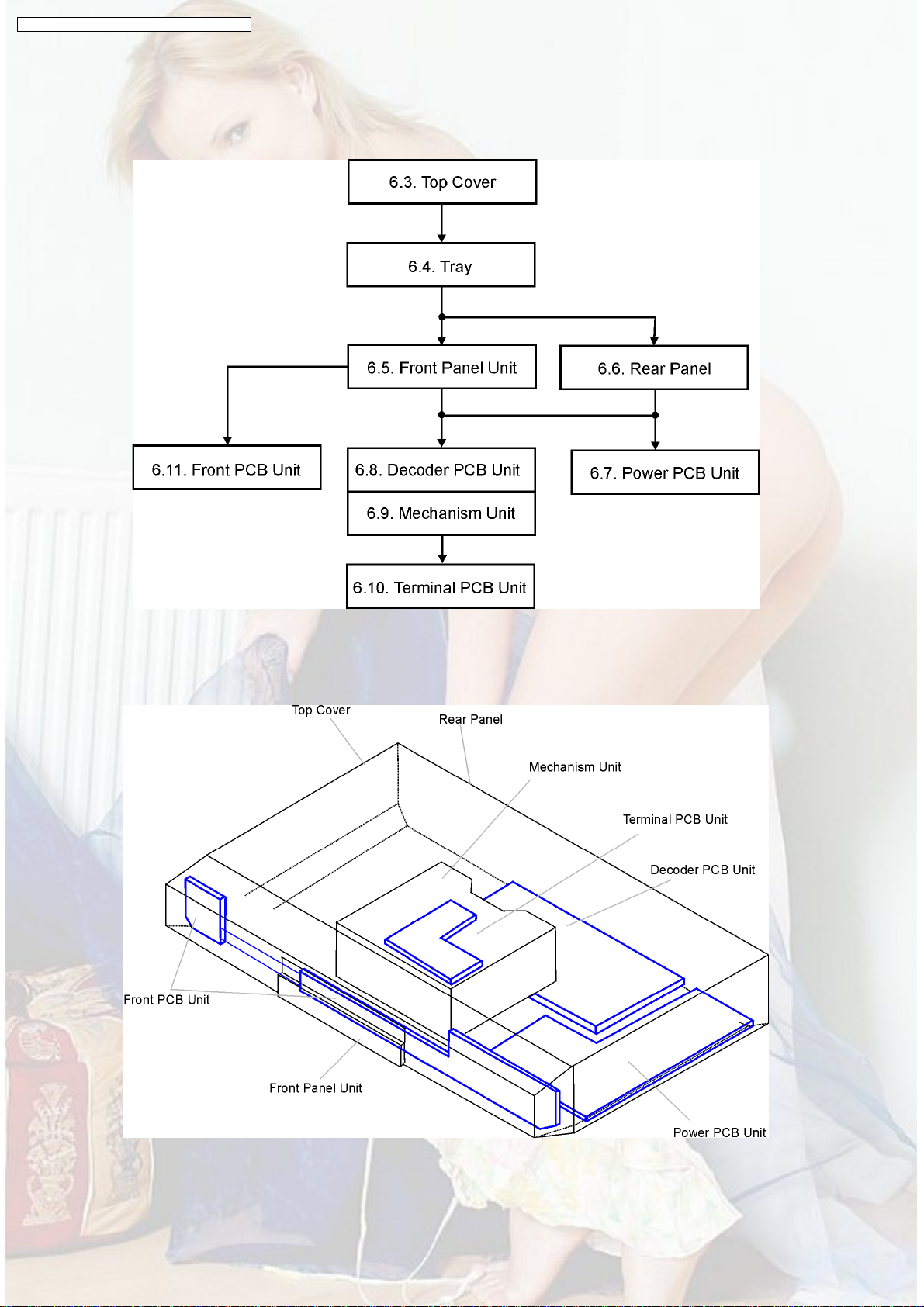
6 Disassembling the Casing and Checking PCBs 8
6.1. Dissasembly Procedure 8
6.2. Casing Parts and PCB Positions 8
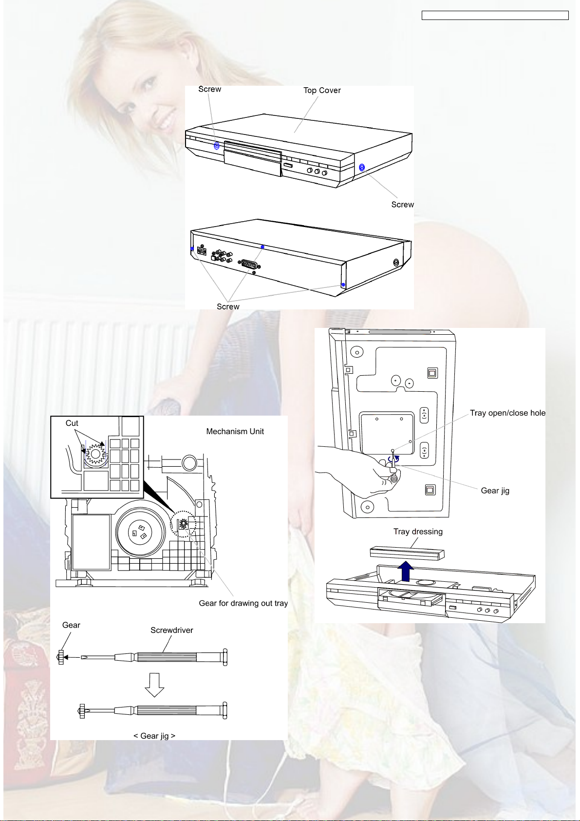
6.3. Top Cover 9
6.4. Tray 9
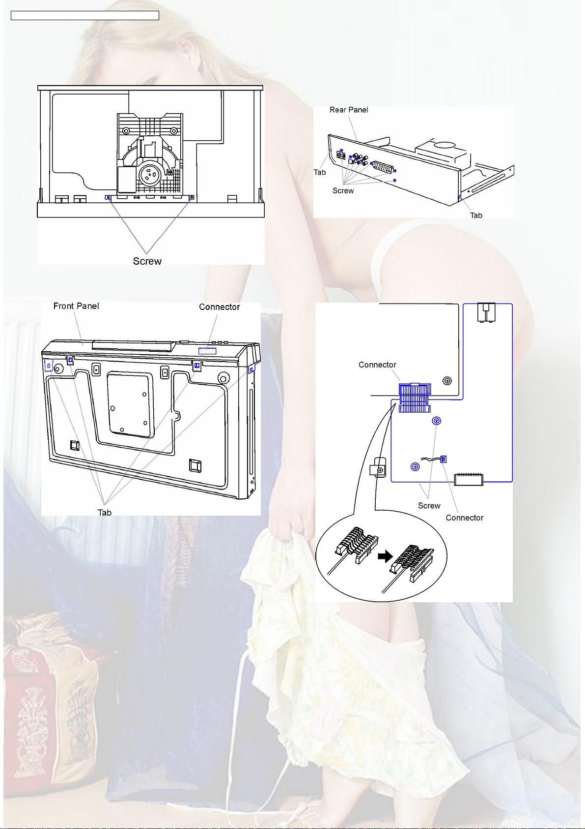
6.5. Front Panel Unit 10
6.6. Rear Panel 10
6.7. Power PCB Unit 10
6.8. Decoder PCB 11
6.9. Mechanism Unit 11
6.10. Terminal PCB 11
6.11. Front Panel PCB Unit 11
6.12. Servicing Position 12
7 OPTICAL PICKUP SELF-DIAGNOSIS AND REPLACEMENT
PROCEDURE 13
7.1. Self-diagnosis 13
7.2. Cautions to be used before replacing the Optical Pickup
Unit and Spindle Motor assembly 14
8 Self-Diagnosis Function and Service Modes 15
8.1. Service Mode Table 1 15
8.2. DVD Self Diagnostic Function-Error Code 15
8.3. Last Error Code saved during NO PLAY 16
8.4. Service mode table 2 17
8.5. Overview of each function 19
8.6. Sales demonstration lock function 19
8.7. Handling After Completing Repairs 19
8.8. Service Precautions 20
9 ASSEMBLING AND DISASSEMBLING THE MECHANISM UNIT
21
9.1. Disassembly Procedure 21
9.2. Terminal PCB 21
9.3. Clamp Plate Unit 21
9.4. Tray 22
9.5. FG PCB Unit 23
9.6. Traverse Block 23
9.7. Traverse Gear 24
9.8. Optical Pickup Unit 24
9.9. Disassembling the Middle Chassis 29
9.10. Disassembling the Traverse Gear A 29
9.11. Disassembling the Spindle Motor Unit 29
10 ADJUSTMENT PROCEDURES 30
10.1. Service Tools and Equipment 30
10.2. Important points in adjustment 30
10.3. Storing and Handling Test Discs 30
10.4. Optical adjustment 31
11 Abbreviations 32
12 Voltage Chart 34
13 BLOCK DIAGRAM 37
13.1. OVERALL BLOCK DIAGRAM 37
13.2. POWER BLOCK DIAGRAM 38
13.3. FRONT PANEL BLOCK DIAGRAM 39
13.4. SERVO BLOCK DIAGRAM (Decoder PCB) 40
14 SCHEMATIC DIAGRAM 41
14.1. INTERCONNECTION SCHEMATIC DIAGRAM 41
14.2. POWER PCB UNIT 42
14.3. FRONT PANEL PCB UNIT 43
14.4. DECODER INTERCONNECTION 44
14.5. DECODER PCB (AV DECODER) 45
14.6. DECODER DRIVE CONNECTION 46
14.7. DECODER FLASH MEMORY 47
14.8. DECODER AV INTERFACE 48
14.9. DECODER AUDIO DAC 49
14.10. TERMINAL PCB 50
15 PRINT CIRCUIT BOARD 51
15.1. Decoder PCB Unit 51
15.2. Power PCB Unit 52
15.3. TERMINAL PCB 53
15.4. Front PCB Unit 54
16 EXPLODED VIEWS 55
16.1. Casing Parts& Mechanism Section Exploded View 55
16.2. Mechanism Section Exploded View 56
16.3. Packing& Accessories Section Exploded View 57
17 REPLACEMENT PARTS LIST 58
18 All Schematic Diagram for printing with A4 64
CONTENTS
Page Page
2
DVD-S35E / DVD-S35EB / DVD-S35EG / DVD-S31EG