1 Safety Precaution 3
1.1. General guidelines 3
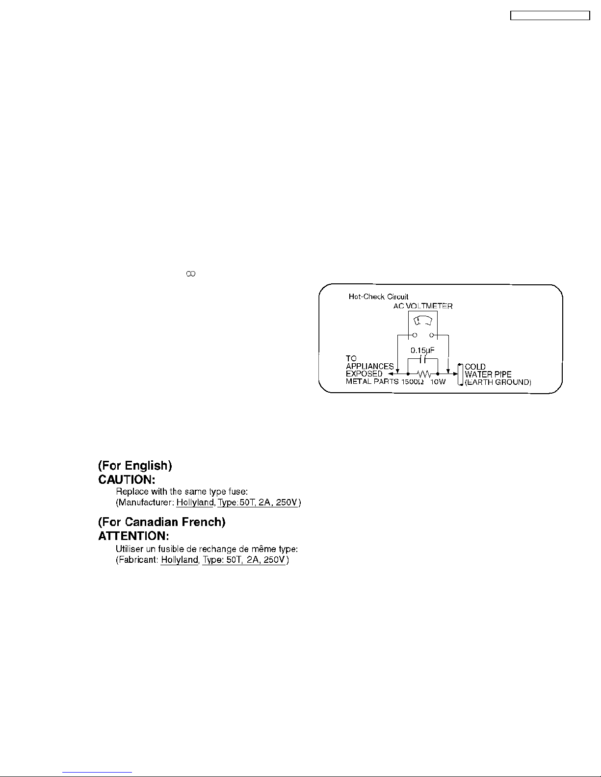
1.2. Caution for fuse replacement 3
2 Warning 4
2.1. Prevention of Electrostatic Discharge (ESD) to
Electrostatic Sensitive (ES) Devices 4
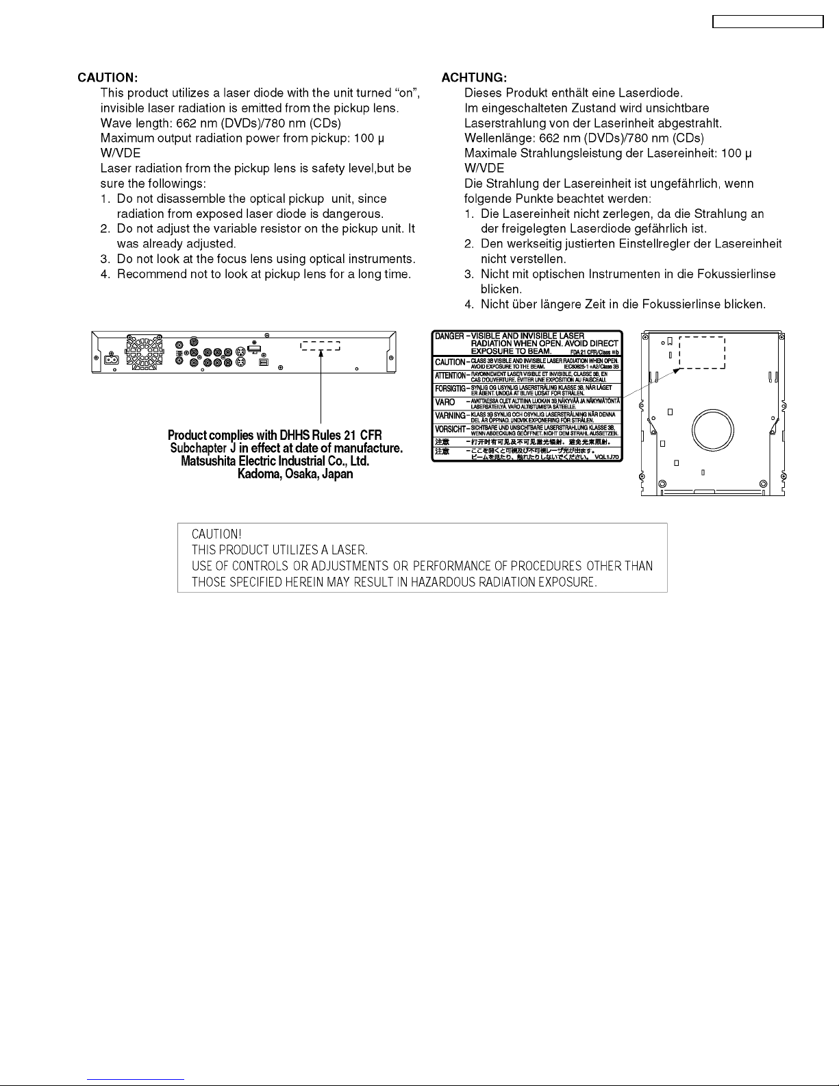
2.2. Precaution of Laser Diode 5
2.3. Service caution based on legal restrictions 6
3 Service Navigation 7
3.1. Service Information 7
3.2. Caution for DivX 7
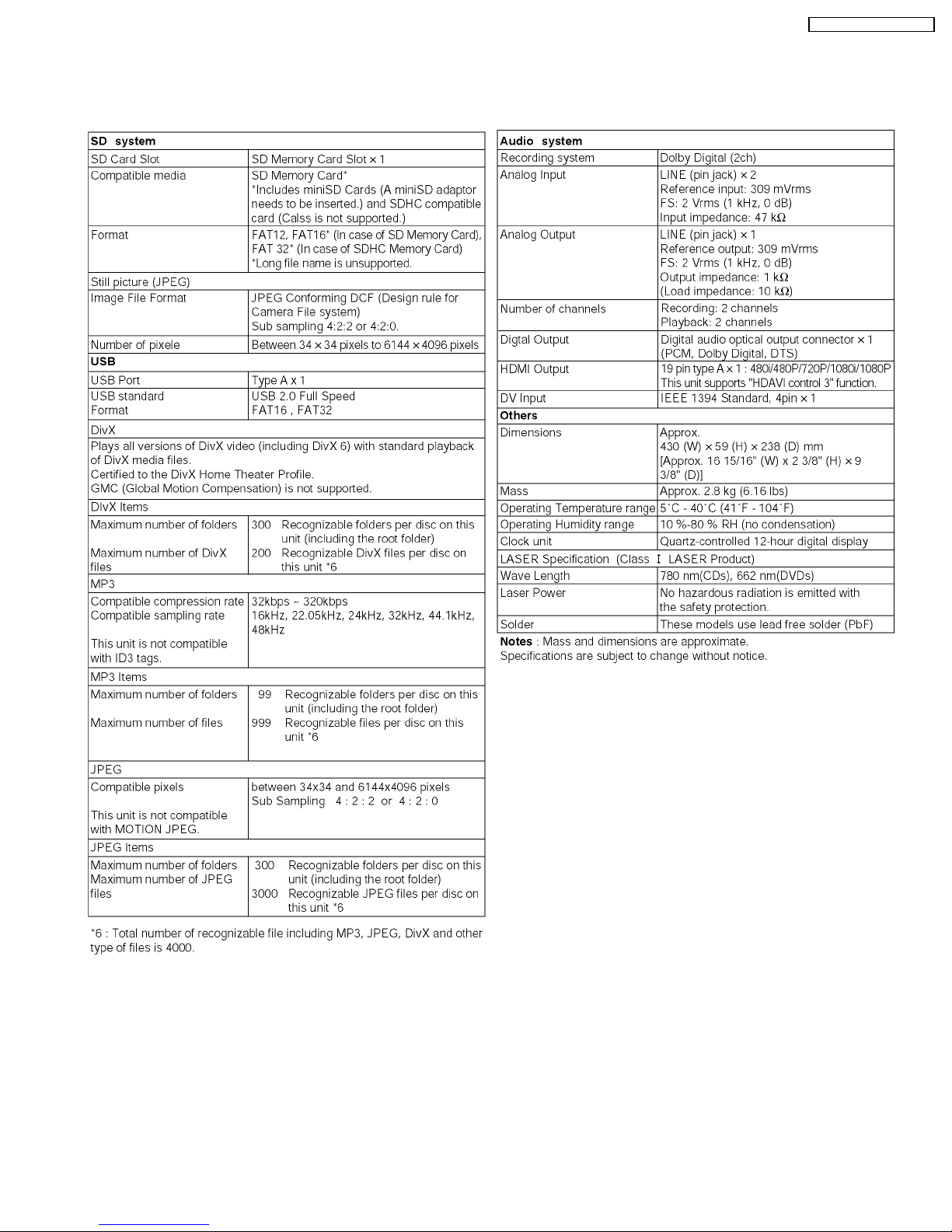
4 Specifications 8
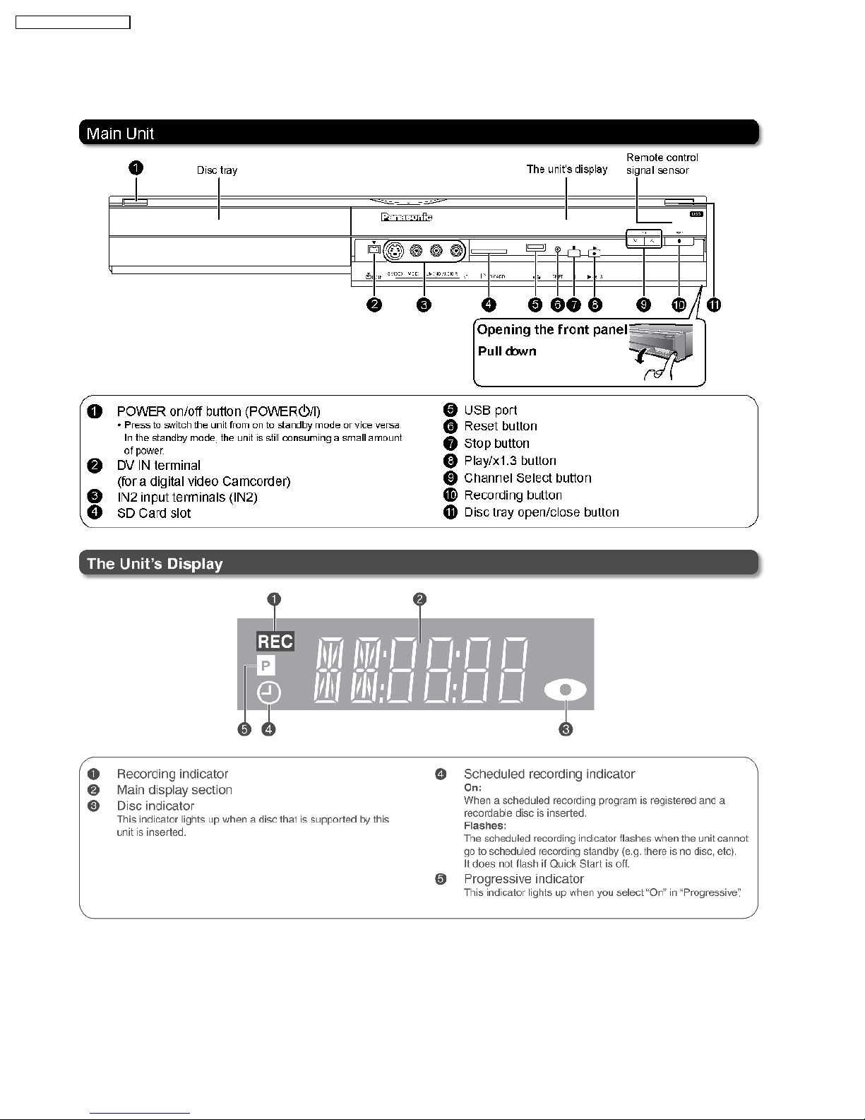
5 Location of Controls and Components 10
6 Operation Instructions 12
6.1. Taking out the Disc from DVD-Drive Unit when the Disc
cannot be ejected by OPEN/CLOSE button 12
7 Service Mode 15
7.1. Self-Diagnosis and Special Mode Setting 15
8 Service Fixture & Tools 25
9 Assembling and Disassembling 26
9.1. Disassembly Flow Chart 26
9.2. P.C.B. Positions 26
9.3. Top cover 27
9.4. Front Panel, Front (R) P.C.B and Front (L) P.C.B. 27
9.5. DV Jack and SD/USB P.C.B. 28
9.6. Rear Panel 28
9.7. Digital P.C.B. 29
9.8. DVD Drive 29
9.9. Main P.C.B. and SW P.C.B. 30
10 Measurements and Adjustments 31
10.1. Service Positions 31
10.2. Notice after replacing Digital P.C.B. 33
10.3. Caution for Replacing Parts 33
10.4. Standard Inspection Specifications after Making Repairs
34
11 Block Diagram 35
11.1. Power Supply Block Diagram 35
11.2. Analog Video Block Diagram 37
11.3. Analog Audio Block Diagram 38
11.4. Analog Timer Block Diagram 39
12 Schematic Diagram 41
12.1. Interconnection Schematic Diagram 41
12.2. Power Supply Section (Main P.C.B. (1/4)) Schematic
Diagram (A) 42
12.3. AV IO (1/4) Section (Main P.C.B. (2/4)) Schematic
Diagram (A) 44
12.4. AV IO (2/4) Section (Main P.C.B. (2/4)) Schematic
Diagram (A) 45
12.5. AV IO (3/4) Section (Main P.C.B. (2/4)) Schematic
Diagram (A) 46
12.6. AV IO (4/4) Section (Main P.C.B. (2/4)) Schematic
Diagram (A) 47
12.7. Tuner Section (Main P.C.B. (3/4)) Schematic Diagram
(TU) 49
12.8. Timer Section (Main P.C.B. (4/4)) Schematic Diagram (T)
50
12.9. DV Jack Schematic Diagram 52
12.10. SD/USB Schematic Diagram 53
12.11. SW Schematic Diagram 55
12.12. Front (L) Schematic Diagram 55
12.13. Front (R) Schematic Diagram 55
13 Printed Circuit Board 57
13.1. Main P.C.B. 57
13.2. Front (L) P.C.B. 62
13.3. Front (R) P.C.B. 62
13.4. DV Jack P.C.B. 63
13.5. SW P.C.B. 63
13.6. SD/USB P.C.B. 64
14 Appendix for Schematic Diagram 65
14.1. Voltage and Waveform Chart 65
14.2. Waveform Chart 67
14.3. Abbreviations 68
15 Parts and Exploded Views 70
15.1. Exploded Views 70
15.2. Replacement Parts List 72
CONTENTS
Page Page
2
DMR-EZ28P / DMR-EZ28PC