Panasonic FZ-10 User manual

ORDER NO. IMD9504003C2
erviceManual
r,[lCDMPACT
rllCOMPACf
wD~©
wD~©
DIGITAL AUDIO
DIGITAL AUDIO
I
GRAPHICS
I
A
WARNING
3D0
Interactive
Multiplayer
FZ-10
This
is
the Service Manual
for the following area.
~
...
for
U.K.
This service information is designed
for
experienced repair technicians only and is not designed
for
use by the general public. It
does not contain warnings or cautions
to
advise non-technical individuals
of
potential dangers in attempting
to
service a product.
Products powered by
electricity
should be serviced or repaired only by experi_enced professional technicians. Any attempt
to
service
or repair the product or products dealt
with
in
this
service information by anyone else could result in serious injury or death.
Panasonic®
© 1994
Matsushita
Electric Industrial Co., Ltd.
All rights reserved. Unauthorized copying and
distribution
is a violation
of
law.

FZ-10
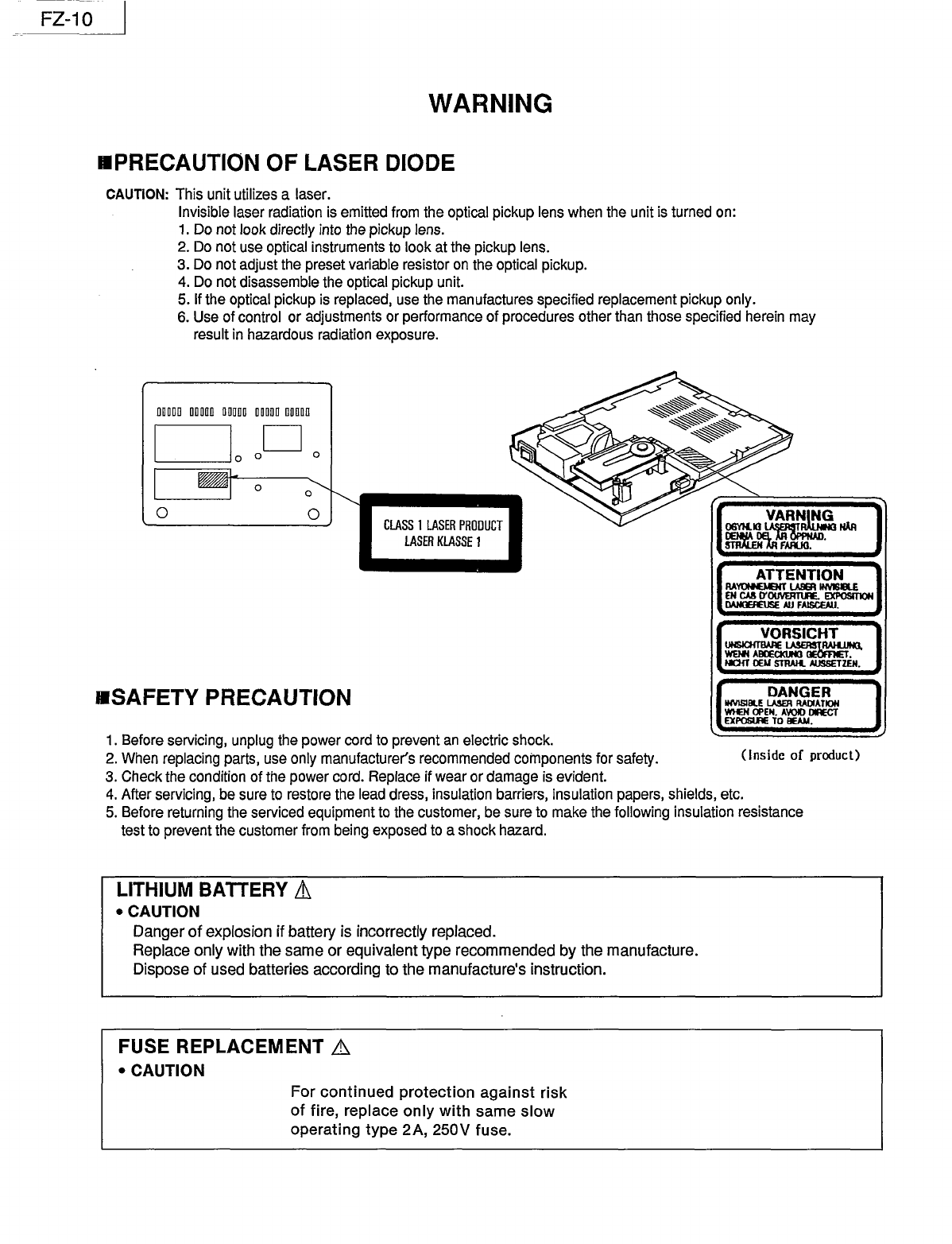
WARNING
■
PRECAUTION
OF
LASER DIODE
CAUTION:
This
unit
utilizes
a
laser.
Invisible
laser
radiation
is
emitted
from
the
optical
pickup
lens
when
the
unit
is
turned
on:
1.
Do
not
look
directly
into
the
pickup
lens.
2.
Do
not
use
optical
instruments
to
look
at
the
pickup
lens.
3.
Do
not
adjust
the
preset
variable
resistor
on
the
optical
pickup.
4.
Do
not
disassemble
the
optical
pickup
unit.
5.
If
the
optical
pickup
is
replaced,
use
the
manufactures
specified
replacement
pickup
only.
6.
Use
of
control
or
adjustments
or
performance
of
procedures
other
than
those
specified
herein
may
result
in
hazardous
radiation
exposure.
om
□
omo
DODOO
DODOO
DDDDll
D
0 0
0 0
0 0
■
SAFETY
PRECAUTION
CLASS
1
LASER
PRODUCT
LASER
KLASSE
1
1.
Before
servicing,
unplug
the
power
cord
to
prevent
an
electric
shock.
YARNING
06YII.IO~NAA
~~FAR.IO
..
ATTENTION
RAYONEMEHT
LABER
IIMUllE
EH
CM
O'OU\IERT\IE.
EXPOSmON
DANClEAEIJSE
All
FAISCEAU.
VORSICHT
UNSICHTIWlE
I..ASERSllWUJNO.
WElft
~
BEOmET.
IIClf1'
OEM
STRAK.
AUSSETZEH.
DANGER
IIMSIII.!
LASER
RADIATION
WIEH
OPEii.
AYOIO
DIRECT
EXPOSlflE
TO
BEAM.
2.
When
replacing
parts,
use
only
manufacturer's
recommended
components
for
safety.
Onside
of
prcxlucl)
3.
Check
the
condition
of
the
power
cord.
Replace
if
wear
or
damage
is
evident.
4.
After
servicing,
be
sure
to
restore
the
lead
dress,
insulation
barriers,
insulation
papers,
shields,
etc.
5.
Before
returning
the
serviced
equipment
to
the
customer,
be
sure
to
make
the
following
insulation
resistance
test
to
prevent
the
customer
from
being
exposed
to
a
shock
hazard.
LITHIUM BATTERY &
• CAUTION
Danger
of
explosion ifbattery is incorrectly replaced.
Replace only with the same or equivalent type recommended by the manufacture.
Dispose of used batteries according to the manufacture's instruction.
FUSE REPLACEMENT A
• CAUTION For continued protection against risk
of
fire, replace only
with
same
slow
operating type 2A, 250V fuse.

Warning
FOR YOUR SAFETY PLEASE READ THE FOLLOWING TEXT CAREFULLY
This appliance
is
supplied with a moulded three pin mains plug for your safety and conve-
nience.
A 3
amp
fuse
is
fitted in this plug.
Should thefuse need to be replaced please ensure that
the
replacement fuse has a rating of
3
amps
and that it
is
approved by ASTA
or
BSI
to
BS1362.
Check for the ASTA
mark~
or
the
BSI
mark~
on
the
body of the fuse.
Ifthe plug contains a removable fuse cover you must ensure that
it
is
refitted when the fuse
is
replaced.
Ifyou lose the fuse cover the plug must not be used until a replacement cover
is
obtained.
A replacement fuse cover can be purchased from your local Panasonic Dealer.
IF
THE FITTED MOULDED PLUG
IS
UNSUITABLE FOR THE SOCKET OUTLET
IN
YOUR HOME THEN THE FUSE SHOULD
BE
REMOVED AND THE PLUG CUT OFF
AND DISPOSED OF SAFELY.
THERE
IS
A DANGER
OF
SEVERE ELECTRICAL SHOCK
IF
THE CUT OFF PLUG
IS
INSERTED INTO ANY
13
AMP SOCKET.
Ifa new plug
is
to be fitted please observe
the
wiring code as shown below.
Ifin any doubt please consult a qualified electrician.
Important
The
wires in this mains lead are coloured
in
accordance with the following code:
Blue: Neutral
Brown: Live
As the colours of thewires in the mains lead of this appliance may not correspond with
the
coloured markings identifying the terminals in your plug, proceed as follows:
The
wire which
is
coloured BLUE must be connected to
the
terminal in the plug which
is
marked with the letter N
or
coloured BLACK.
The
wire which
is
coloured BROWN must be connected
to
the terminal in the plug which
is
marked with the letter L
or
coloured RED.
Under no circumstances should either of these wires be connected to the earth terminal of
the three pin plug, marked with the letter E
or
the Earth Symbol
~
.
■
How
to
replace
the
fuse
Open
the fuse compartment with a screwdriver and
replace the fuse.
This equipment
is
produced to
BSS00/1983.
The
unit
is
in the standby condition when the AC power
supply cord
is
connected.
The
primary circuit
is
always "live" as long asthe power
cord
is
connected to
an
electrical outlet.
Fuse
FZ-10

FZ-10
Contents
1.
System
Overview
1-1.
General
Description
........................:.......................................
1-1
1-2.
Specifications ..........................................................................
1-1
1-3.
Location
of
Control
and
Components
.....................................
1-2
1-4.
Block
Diagram
........................................................................
1-4
1-5.
Block
Explanation
...................................................................
1-6
2.
Checking
Information
2-1.
Handling
Precautions
for
Traverse
Deck
................................
2-1
2-2.
Disassembly
/
Reassembly
....................................................
2-2
2-3.
Troubleshooting
Table
............................................................
2-5
2-4.
Terminal
Function
of
IC's
........................................................
2-6
3.
Diagrams
and
Replacement
Parts
List
3-1.
Wiring
Connection
diagram
....................................................
3-1
3-2.
Schematic
Diagrams
..............................................................
3-2
3-3.
Printed
Circuit
Boards
.............................................................
3-1
O
3-4.
Service
Notes
and
Precaution
................................................
3-13
3-5.
Service
Tools
..........................................................................
3-14
3-6.
Exploded
Views
and
Replacement
Parts
List.........................
3-15
3-
7.
Electrical
Replacement
Parts
List
...........................................
3-16

FZ-10
1.
System
Overview
1-1.
General
Description
The
FZ-10
is
the
same
function
as
FZ-1.
The
FZ-10
is
adopted
Top
Loading
System
and
includes a
CD-ROM
drive circuit into the
Main
PCB.
1-2.
Specifications
CPU
32-bit
RISC
orocessor
ARM60
(12.5
MHz)
Memory
RAMNRAM 3
MB
(Total)
2
MB:
Main-RAM
1 MB:VRAM
SRAM
32
KB
(Batterv
back
uo)
ROM
1
MB
DSP
(Digital
Signal
Processor)
Original 16-bit digital
signal
processor
Video/
Audio
Video
output
Composite
video,
PAL
S-Video,
PAL
RF
Video,
PAL,
Channel
21
Resolution
768
(H)
x
576
(V)
dots (Inside
384
x
288
dots)
Colors
Max.
16.7 Million/
Std.
32K
Audio
Stereo
16-bit
PCM
(Samplina:
44.1
kHz}
Storage
CD-ROM
drive
Size:
12
and
8
cm
(CD
single)
Double
Soeed
CD-ROM
Drive
(Read
Buffer:
32
KB)
Extension
memory
(via
Expansion
Port)
1/0
Port
Control
port
Low
speed
1/0:
Dsub
9-pin
x 1
Daisv-chain
svstem
Expansion
port
Hiah
speed
1/0:
30-pin
x 1
AV
Expansion
port
Hiah
speed
AV-I/O
(Video
CD
Adaptor):
68-pin
x 1
System
System
dimensions
310
x
236
x
68
mm
(12.2
x
9.3
x
2.7
inch)
(Wx
Dx
H}
Weiaht
1.7
ka
(3.8
lb)
Power
reauirement
230
-
240
V
AC
50
Hz
Power
consumotion
30W
Indicator
Power
indicator
Red-LED
x 1
CD-access
indicator
Green-LED
x 1
Temperature
Ooeratina
10°c
to
35°C
(50°F
to
95°F)
Storage
-20°C
to
60°C
(-4°F
to
140°F)
(When
packed
for
shipment)
FMV:
Full
Motion
Video
1-1

1-3.
Location
of
Control
and
Components
•
Front
View
•
Rear
View
Controlier
port
(CONTROLLER)
Dedicated
port
for
the
provided
controller.
Ready
indicator
(READY)
Lights
up
when
power
is
on.
RF
output socket
(RF
OUT)
When connecting with a television
which does not have
an
audio/video
socket, the provided
RF
cable is
used.
S-video
output
socket---~
(S-VIDEO
OUT)
CD
access
indicator
(ACCESS)
AV
expansion
slot
(AV-EXPANSION)
Dedicated
slot,
visible
upon
opening
the
cover,
used
with
separately
sold
FMV
cartridges.
Lights
up
when
CD
is
being
accessed.
Expansion
Port
(EXPANSION)
Slot
for
peripheral
devices
which
utilize
high
speed
data
transfer.
Power
switch
(POWER)
When
using
a
television
which
supports
S-video,
connecting
a
separately
sold
S-video
cable
results
in
a
sharper
picture.
Right/Left audio output socket
(AUDIO
OUT
R/L)
Video output socket
(VIDEO
OUT)
1-2
•
Controller
Connector
Connected
to
the
Multiplayer
unit.
Left shift
button
(L)
Directional
buttons
X
button
(X)
1-3
I FZ-10
-
'--------
----
-------
Extension
port
(EXTENSION)
Participation
by
more
than
one
player
is
achieved
by
connecting
aseparately
sold
controller
to
this
port.
A,
B
and
C
buttons
(A,
B,
C)
Play/Pause
button
(P)

FZ-10 FZ-10
1-4. Block Diagram
Traverse Unit I
J,
.
OPEN/CLOSE Switch Power Switch
SW720
,.
-0-------1
-------------------------------------------------------
-----L~----
- - - -
------
- - -
-1
Vdd +5V CN762 CN760 •l CN761 •l
CN720:
CN0010
Lithium
' I
cs
I
Battery IC760 IC720 I
I S.Motor Power Supply I
AN8388SR-E2 AN8803NSB-E2 I I
BT400 Control Circuit I
Q Motor Driver Head AMP I
I
IC100 IC350 IC400 I
f I
DAP60ARM-X1 K IC340 DA58257AM2TS DABA6162FT2E CN101 I
Masked ROM
LJ
I I
CPU SAAM Backup Control ' .
rr-------'
:_
--------1
• '
'l
IC650 -IC700IC640 CN420 1
Address DA2A256SM7TW
~
DA9800KV26V MN662710RA I
' DATA Buffer Error Correction Servo Processor CN620 1
I
i-._
,.
+5V +9V
~
,,
Data f !
I -•
f
.~
Slow BUS -
, ) I
I I IC600 IC660
.~
DA623851 PVJ
~
MN1882410FZA
CD-ROM Interface 1-chip Microprocessor CNsoo';--
Gate Array
,....,__
-
X151
' , f
50.0MHz I
SYSTEM CLOCK
~
~
X153
IC120 59.0MHz
MN7B003ABK -
T
ANVIL VIDEO CLOCK CN500 1
--'--
LIC200 IC220 Q260,Q261,Q262
~
/ 32 DA431 0VME2XQ I-.- DANJM2902MTP Q263,Q500,Q501
/ 32 , Audio DAC Audio Amp.
I-
Mute Circuit
Address Serial Data
.--
---
---
---
--
-------------------- -----------------------
' '
' '
' '
O1ao,orn1,O1a4
I
Data ' ' I ' ©
'
;.
;.
I ' Video Amp. I
'
' ' I '
'
' '
2M-bit VRAMx4 '
-' ' '
-' ' ' ©
' ' IC300,301,320,321 '
...
' ' '
::-
' ' '
Cl
0
' ' '
'
• • '
'
I '
' ---,--
I '
'
-L
{ I ' Monaural
'
4M-bit DRAMx4 ' IC520 @
' -
'
IC310,311,330,331 ' Composit~ ENC-37454
'
' RF Modulator
'.
' -
'
'---------------------------------------------------------
CN900i
-...:../.
I
-------------------------------------------------------------------------------------------------------------------J
1-4
1-5
AC
EXPANSION PORT
(30-pin)
AV EXPANSION PORT
(FMV CARTRIDGE
INTERFACE)
(68-pin)
RIGHT/LEFT AUDIO
OUTPUT
JACK
VIDEO
OUTPUT
JACK
S-VIDEO OUTPUT
JACK
RF MODURATED
VIDEO
OUTPUT
CONTOROLLER PORT
(9-pin D-sub)

1-5.
Block
Explanation
CPU
CPU is ARM60. This RISC type micro processor has 32-bit address and 32-bit data path.
MADAM
supplies CPU with 12.5 MHz clock.
ROM
1 MB
ROM
stores the system management program. The
ROM
is
connected
to
Slow bus and its data
is
read by
MADAM and MADAM arranges 8-bit data into 32-bit word and send it
to
CPU.
SRAM
32
KB
SRAM is connected to Slow bus. Since Lithium battery backs up SRAM while power is down,
SRAM can retain data. It may be used to back up game data, for example.
DRAM/VRAM
DRAM and VRAM is used as main memory.
VRAM is dual-port memory. This means one port
is
used
as
normal DRAM and the other one
is
used to read and write
data simultaneously with the former port. Therefore, it
is
used as Frame Buffer which
is
required fast access.
ANVIL
This
system
IC
includes
MADAM,
CLIO (the
system
IC's
for
FZ-1) and a
digital
color
encoder.
ANVIL
has
the
following
functions.
CPU
control:
ANVIL
drives
control
signals
for
the
CPU.
Memory
management:
ANVIL
controls
access
to
DRAM's
and
VRAM's.
Cell
engin:
ANVIL
manages
cells
(objects
on TV screen).
DSP:
ANVIL
includes
a
digital
signal
processor,
which
deals
with
sound.
Video
signal
output:
ANVIL
outputs
video
signals
(composit,
Y and C).
AudloDAC
16-bit Audio DAC converts digital audio data from CLIO into analog audio data.
CLIO sends DAC datawith serial communication manner.
CD-ROM interface
CD-ROM interface Gate Array
is
the interface between CLIO and both internal CD-ROM drive and External drives which
are connected through Expansion Port.
1-6

FZ-10
Error
Correction
This
is
ablock
for
error
correction,
and
transferring
data
and
commands.
A
command
data
which
comes
from
Main
unit
goes
to
1-chip microprocessor via
the
interface
for
CD-ROM.
The
data
stored
on
adisk
go
through
a
data
servo
proces-
sor
serially.
Once
the
data
will
be
stored
in
the
data buffer
and
it
will
be
checked
and
corrected
if it
is
identified
as
a
false
data.
Then
it
go
out
to
the
CD-ROM
interface.
Data
Buffer
32K
SRAM
memory
is
used
to
store
data
from
CD-ROM
temporarily.
1-chlp
Microprocessor
1-chip
microprocessor
is
for
processing
commands
from
the
main
system.
Digital
Servo
Processor
Digital
Servo
Processor
have
some
functions
as
optical
servo(
focus,
tracking
and
traverse
servo}
process,
digital pro-
cess
(EFM
modulation,
error
correction)
and
digital
servo
process
for
S.Motor.
The
optical
servo
will
not
require
adjust-
ment
for
its
gain,
offset,
and
balance
manually
because
it
does
all
automatically.
The
Digital
processing
block
provides
digital
signal
based
on
RF
signal,
and
send
to
the
error
correction
IC.
Motor
Driver
As
the
analog
control
signal
from
digital
servo
processor,
Motor
Driver
supply
atraverse
motor,
focus
actuator of pick
up
unit
and
tracking
actuator
with
electrical
power.
S.Motor
Control
As
the
control
signal
from
digital
servo
processor ,S.Motor
control
circuit generates a
signal
to
control
the
speed
of
the
S.Motor.
1-7

2.
Checking Information
2-1.
Handling
Precautions
for
T1raverse
Deck
The
laser
diode
in
the
traverse
deck
(optical
pickup)
may
break
down
due
to
potential
difference
caused
by
static
electricity
of
clothes
or
human
body.
So,
be
careful
of
electrostatic
breakdown
during
repair
of
the
traverse
deck
(optical
pickup).
•
Handling
of
traverse
deck
(optical
pickup)
FPC boards
FZ-10
1.
Do
not
subject
the
traverse
deck
(optical
picl<up)
to
static electricity
as
it
is
extremely
sensitive
to
electrical
shock.
Lens {Do not touch) {Handle then carefully)
2.
To
prevent
the
breakdown
of
the
laser
diode,
an
antistatic
shorting
pin
is
inserted
into
the
flexible
board
(FPC
board).
When
removing
or
connecting
the
short
pin,
finish
the
job
in
as
short
time
as
possible.
3.
Take
care
not
to
apply
excessive
stress
to
the
flexible
board
(FPC
board).
4.
Do
not
turn
the
variable
resistor
(laser
power
adjustment).
It
has
already
been·adjusted.
I
Traverse Deck Variable resistor
Be
sure
to
short this portion
(Do not touch) {Use
the
shorting
pin
or
clip)
Wrist strap
(Anti-static bracelet)
•
Grounding
for
electrostatic
breakdown
prevention
1.
Human
body
grounding
Use
the
anti-static
wrist
strap
to
discharge
the
static electricity
from
your
body.
2.
Work
table
grounding
Put
a
conductive
material
(sheet)
or
steel
sheet
on
the
area
where
the
optical
pickup
is
placed,
and
ground
the
sheet.
Caution:
The
static electricity
of
your
clothes
will
not
be
grounded
through
the
wrist
strap.
So,
take
care
not
to
let
your
clothes
touch
the
traverse
deck
(optical
pickup).
2-1
Iron
plate
or some metals
to conduct electricity

FZ-10
I
2-2.
Disassembly
/
Reassembly
Note:
Before
disassembling,
be
sure
to
perform
the
following
procedures
first.
1.
Remove
the
CD-ROM
disk if it
is
inserted
in
the
CD-ROM
drive.
2.
Turn
the
power
switch
off.
3.
Disconnect
the
AC
power
cord.
4.
Remove
the
optional
units.
Caution:
Please
follow
directions
carefully.
Do
not interchange
screws
in
any
part of
the
system.
•
Reassemble
in
the
reverse
order
Top
Case
Figure
1
Traverse
Unit
Pin
<B>
Pin<B>
Figure
2
Insulator
Figure
3
(1)
Turn
this
unit
(FZ-10)
upside
down
and
place
it.
(2)
Remove
seven
screws
<A>
as
shown
in
figure
1.
(3)
Turn
it
over
again
and
gradually
raise
the
top
case.
(1)
After
removing
the
top
case,
remove
the
two
pins
<B>
as
shown
in
figure
2.
(Push
from
the
bottom
side.)
(2)
Remove
the
traverse
cover.
(3)
Gradually
raise
the
traverse
unit
and
then
disconnec_t
the
five
connectors
as
shown
in
figure
3.
(4)
Remove
the
traverse
unit.
2-2

C760
Power PCB
Main PCB
0
Figure
4
Figure
5
LED guide panel
Figure
6
CN420
Figure
7
FMV
cover
2-3
Fz.:10
Caution:
Reassembling,
be
sure
to
arrange the
lead
wire
for
CN762
in
figure
4.
(1)
After removing
the top
case,
remove
the
Power
PCB
cover.
(2)
Unlock
the
four
hooks
<C>
and
remove
the
AC
inlet
terminal-and
remove
power switch
as
shown
in
figure
5.
(3)
Remove
the
two
screws
<D>.
(4)
Disconnect
the
connector
(CN101)
and
remove
the
Power
PCB.
(1)
After removing
the top
case
and
traverse
unit,
remove
the
LED
guide panel.
(2)
Remove
five
screws
<E>
and
then
remove
the
upper
shield
plate
as
shown
in
figure
6.
(3)
Remove
the
FMV
cover
at
right side.
(4)
Remove
the
two
screws
<F>
as
shown
in
figure
7.
(5)
Disconnect the connector
(CN420)
and
then
remove
the
Main
PCB.

FZ-10
CD Panel
DC
Latch
m
Figure
8
Oil
damper
Figure
9
Figure
10
(1)
After
removing
the
top
case,
unlock
two
hooks
<G>
as
shown
in
Figure
8.
(2)
Remove
the
CD
Panel
unit.
(3)
Remove
the
hop-up
spring
and
oil
dumper
as
shown
in
figure
9.
(4)
remove
the
CD
Panel.
(1)
After
removing
the top
case,
unlock
two
hooks
<H>
at
reverse
side
of
the top
case
as
shown
in
figure
10.
(2)
Remove
the
DC
Latch.
2-4

2-3.
Troubleshooting
Table
Picture,
Sound
Symptom
No
picture
and
no
sound
No
sound
Loud
noise
appear
or
sound
disappear
at
random,
and
they
are
repeatable.
Sound
is
stoooed
accidentally.
Color
is
abnormal.
Object
(such
as
a meteorite
in
the
demo-screen)
is
abnormal.
Although
the
image
had
be
cleared
already,
it
have
remained
on
the
screen.
Operation
Symptom
Particularly
program
is
not
executed.
Program
is
stopped
during
the
execution
and
it
is
repeatable.
Proo
ram
is
stoooed
accidentally.
Picture
becomes
stop-motion
playina.
Prooram
is
stoooed
at
random
and
it
is
repeatable.
2-5
FZ-10
Cause
Resistor
array
which
is
connected
to
DRAM
is
solder_ed
not
enough.
IC31
0
and
IC330
are
abnormal.
IC300,
IC301,
IC320
and
IC322
are
abnormal.
One
of
IC120
and
IC1
00
is
abnormal.
Circuit pattern
around
IC120
and
IC1
00
is
cut.
Circuit pattern
around
DRAM
is
cut.
MUTE
circuit(O500, 0501, 0263, 0262, 0261
and
0260)
is
abnormal.
If
base
voltage of 0500
is
set
high,
MUTE
circuit
is
abnormal.
IC120
(ANVIL)
Traverse Unit
Each
signal
[S0-S31:
between
ANVIL
and
DRAM]
is
abnormal.
IC120
(ANVIL)
is
abnormal.
IC120
(ANVIL)
VRAM
(IC300,
IC301,
IC320,
IC321)
is
abnormal.
Cause
IC120
(ANVIL)
Traverse Unit
IC120
(ANVIL)
Traverse Unit
VRAM
(IC300,
IC301,
IC320,
IC321)
IC120
(ANVIL)

FZ-10
2-4.
Terminal
Function
of
IC's
IC100
CPU
I
PIN:
DA86C0602XV\
Pin No. 1/0 Pin Name Comment
1 1/0, TTL D27 Data Bus 27
2 1/0, TTL D28 Data Bus 28
3 1/0, TTL D29 Data Bus 29
41/0,
TTL D30 Data Bus 30
5 1/0, TTL
D31
Data Bus
31
6 lnout, TTL CPA CO orocessor Absent
7 Vss Ground
8 Vdd Power sunnlv
9 Out LOCK Locked operation
10 Input, TTL BIGEND Bia Endian confiauration
11
Out CPI- CO orocessor Instruction
12 Input, TTL DBE Data Bus Enable
13 Out WORD
Bvte-/
Word
14
Input, TTL MCLK Memorv Clock input
15 lnout, TTL WAIT- Wait sianal inout
16 lnout, TTL LATEABT Late Abort inout
17 lnout, TTL PROG32 32-bit Proqram confiquration
18 lnout, TTL DATA32 32-bit Data confiquration
19 Out WRITE Read- I Write
20 Out OPC- One-code fetch
21
Out MREQ- Memorv Request
22 Out SEQ Seauential address
23 Input, TTL ABORT Memorv Abort inout
24 lnout, TTL IRQ- lnterruot Request inout
25 lnout, TTL FIRQ- Fast lnterruot Reauest input
26 lnout, TTL RESET- Reset siqnal input
27 l/O, TTL ALE Address Latch Enable
28 1/0, TTL CPB CO orocessor Busv
29 1/0, TTL TRANS- Memorv Translation
30 Out
A31
Address
31
31
Out A30 Address 30
32 Out A29 Address 29
33 Out A28 Address 28
34 Out A27 Address 27
35 Out A26 Address 26
36 Out A25 Address 25
37 Out A24 Address 24
38 Out
A23
Address 23
39 Out A22 Address 22
40 Out
A21
Address
21
41
Out A20 Address 20
42 Out A19 Address 19
43 Out A18 Address 18 .
44 Out A17 Address 17
45 Out A16 Address 16
46 Out A15 Address 15
47 Out A14 Address 14
48 Out A13 Address 13
49 Out A12 Address 12
50 Out
A11
Address 13
51
Vdd Power supply
52 Vss Ground
53 Out A10 Address 10
54 Out
A9
Address 9
55 Out A8 Address 8
56 Out A7 Address 7
57 Out
AG
Address 6
58 Out A5 Address 5
59 Out
A4
Address 4
Continued (IC100\
Pin No. l/O Pin Name Comment
60
Out
A3
Address 3
61
Out
A2
Address 2
62 Out
A1
Address 1
63
Out
AO
Address 0
64 Vss Ground
65
Vdd Power suoolv
66
lnout, TTL ABE Address Bus Enable
67 Input, TTL, TCK Test Clock
w/ oull-uo
68
Input, TTL, TMS Test Mode Select
w/ oull-uo
69 Input, TTL, TRST- Test Mode Reset
wt
pull-up
70 Input, TTL, TDI Test Data Input
wt
pull-up
71
Out TOO Test Data Outout
72 1/0, TTL
DO
Data Bus 0
73
1/0, TTL
D1
Data Bus 1
74 1/0,
TTL
D2 Data Bus 2
75 l/O, TTL
D3
Data Bus 3
76 1/0, TTL D4 Data Bus 4
77 1/0, TTL D5 Data Bus 5
78 1/0,
TTL
D6 Data Bus 6
79 1/0, TTL D7 Data Bus 7
80 Vss Ground
81
Vdd Power suoolv
82 l/O, TTL D8 Data Bus 8
83 1/0, TTL
D9
Data Bus 9
84 1/0, TTL D10 Data Bus 10
85 1/0, TTL
D11
Data Bus
11
86 1/0, TTL D12 Data Bus 12
87 1/0, TTL D13 Data Bus 13
88 1/0,
TTL
D14 Data Bus
14
89 l/O, TTL D15 Data Bus 15
90 l/O, TTL D16 Data Bus 16
91
1/0, TTL D17 Data Bus 17
92 l/O, TTL D18 Data Bus 18
93 l/O, TTL D19 Data Bus 19
94 l/O, TTL D20 Data Bus 20
95 1/0, TTL
D21
Data Bus
21
96 1/0, TTL D22 Data Bus 22
97 1/0, TTL D23 Data Bus 23
98 1/0,
TTL
D24 Data Bus 24
99
1/0,
TTL D25 Data Bus 25
100 1/0, TTL D26 Data Bus 26
IC120
System IC ANVIL (P/N: MN7B003ABK)
Pin
No.
1/0 Pin
Name
Comment
1 AGND
Analog
ground
20
COMPOUT
Inverted
composite
video
signal
3 AGND
Analog
ground
40
YOUT
Luminance
video
signal
5 VDD Power
supply
6 GND
Ground
7 VDD Power
supply
8 GND
Ground
90
AUDOUT
Digital
audio
data
10 0 RESET"
Master
system
reset
2-6

Continued (IC120) Continued (IC120)
Pin
No.
1/0 Pin Name Comment
Pin
No.
1/0 Pin Name Comment
11
I
TSMODEO
Factory
test
signal 0 54 I LQSF Split register active side
indicator
12 I
TSMODE1
Factory
test
signal 1
for
VRAM and DRAM (data bits
13 I
PBDIN
Data
input
from
3D0
controllers
[31
:161)
14
VDD Power supply
15 0 PBCLK Control port
clock
55 0 LA10 Address 10
for
the left DRAM and
VRAM (data bits
[31
:16])
16 0
PBDOUT
Data
output
to
3D0
controllers
17 0
UNCACKW
Video DMA acknowledge signal
18
GND
Ground
19 I
XACLK
Master audio
clock
from audio
DAG
20
VDD
Power supply
21
0
UNCACKR
Video OMA acknowledge signal
22
0
EXTACKW
Audio DMA
write
acknowledge
signal
23
0
EXTACKR
Audio DMA read acknowledge
signal
24
GNP
Ground
25 I
XVIN
Crystal
input
for
video
clock
26 0 XVOUT Crystal
output
for
video
clock
27
GNP
Ground
56 0 LA9 Address 9
for
the
left
DRAM and
VRAM (data
bits
[31:
16))
57 0
LAB
Address 8
for
the
left
DRAM and
VRAM (data bits
[31
:16])
58 VDD Power supply
59 0
LAO
Address O
for
the
left
DRAM and
VRAM (data bits [31:
161)
60
0 LA7 Address 7
for
the left DRAM and
VRAM (data bits
[31
:161)
61
0
LA1
Address 1
for
the
left
DRAM and
VRAM (data
bits
[31
:161)
62 GND Ground
63 0 LA6 Address 6
for
the left DRAM and
VRAM (data bits [31:
161)
64 0 LA2 Address 2
for
the left DRAM and
28 0
CLC0
CLCO,
1,
2 indicate the type
of
transaction VRAM (data
bits
[31:16])
65 0 LA5 Address 5
for
the
left
DRAM and
29 0
CLC1
CLCO,
1,
2 indicate the type
of
transaction
30 0
CLC2
CLCO,
1,
2 indicate
the
type
of
transaction
31
GND
Ground
VRAM (data
bits
[31
:161)
66
VDD
Power supply
67 0 LA3 Address 3
for
the left DRAM and
VRAM (data bits
[31
:161)
68 0 LA4 Address 4
for
the left DRAM and
32
0 LRAS3* Row address strobe
for
left
DRAM
(data bits
[31
:
161)
33 0 LRAS2* Row address strobe
for
left
DRAM
(data
bits
[31
:
161)
VRAM (data
bits
[31
:161)
69 0 RRAS3* Row address strobe
for
right DRAM
(data
bits
[15:01)
70 GND Ground
34 0 LRAS1* Row address strobe
for
left VRAM
(data
bits
[31:
161)
35 VDD Power supply
36 I
XV251N
Video
clock
input from the
on-board
clock
network
37 0
XV25OUT
Video
clock
output
to
the
on-board
clock
network
38
GND
Ground
39 I
X251N
System
clock
input
71
0 RRAS2* Row address strobe
for
right DRAM
(data bits
[15:01)
72 0 RRAS1* Row address strobe
for
right VRAM
(data
bits
[15:0])
73 0
RRASO*
Row address strobe
for
right VRAM
(data
bits
[15:
01)
74 VDD Power supply
75 0
RSC
Serial VRAM
clock
for
the right
VRAM (data
bits
[15:01)
40
0
X25OUT
System
clock
output
76 0
RSOEO*
VRAM serial port control
output
41
VDD
Power supply enable
42
0
LRASO*
Row address strobe
for
left
VRAM 77 GND Ground
(data bits
[31
:
161)
78
0
RSOE1*
VRAM serial port control
output
43
0
LSC
Serial VRAM
clock
for
the
left
enable
VRAM (data bits
[31
:16)) 79 0 RDTOE* Indicator
of
internal transfer
of
44 0
LSOEO*
VRAM serial port control
output
VRAM (data bits
[15:01)
enable
45
GND
Ground 80 0 RDSF Indicator
of
special
function
of
VRAM (data
bits
[15:0])
46
0 LSOE1* VRAM serial port control
output
81
VDD Power supply
enable 82 0 RCAS* Column address strobe
for
the
right
47
0 LDTOE*
Indicator
of
internal transfer
of
DRAM and VRAM (data
bits
[15:01)
VRAM (data bits [31:
16])
83 0 RWEL* Lower byte
write
enable
for
the
48 0 LDSF Indicator
of
special
function
of
right DRAM
VRAM (data bits
[31
:16]) 84 0 RWEU* Upper byte
write
enable
for
the
49
VDD
Power supply right DRAM
50 0
LCAS*
Column address strobe
for
left
DRAM
and
VRAM
(data
bits
[31
:161)
85
I
RQSF
Split register active side
indicator
for
VRAM and DRAM (data bits
51
0 LWEL* Lower byte write enable
for
the left
[15:01)
DRAM
86 GND Ground
52 0 LWEU* Upper byte write enable
for
the
left
81
0 RA10 Address 10
for
the
right DRAM and
DRAM
VRAM (data bits
[15:01)
53
GND
Ground
2-7

Continued (IC120) Continued (IC120)
Pin
No.
1/0 Pin Name
-··
Comment
Pin
No.
1/0 Pin Name Comment
88 0 RA9 Address 9
for
the
right
DRAM and 133 I S24 VRAM 31-bit serial
bus
data
24
VRAM (data
bits
[15:
01)
134 I
S27
VRAM 31-bit serial bus
data
27
89
0
RAS
Address 8
for
the
right
DRAM and 135 I S26 VRAM 31-bit serial bus
data
26
VRAM (data
bits
[15:01) 136 I
S9
VRAM 31-bit serial bus
data
9
90
VDD Power supply 137 VDD Power
supply
91
0
RAO
Address 0
for
the
right
DRAM and 138 I
S8
VRAM 31-bit serial
bus
data
8
VRAM (data
bits
[15:0]) 139 I
S11
VRAM 31-bit serial bus
data
11
92 0 RA7 Address 7
for
the
right
DRAM and 140 I S10 VRAM 31-bit serial
bus
data
10
VRAM (data
bits
[15:01)
141
I S29 VRAM 31-bit serial
bus
data
29
93 0
RA1
Address 1
for
the
right
DRAM and
VRAM (data
bits
[15:01)
94 GND Ground
95 0 RA6 Address 6
for
the
right
DRAM and
VRAM (data
bits
[15:0])
96
0 RA2 Address 2
for
the
right
DRAM and
VRAM (data
bits
[15:01)
97 0 RA5 Address 5
for
the
right
DRAM and
VRAM (data
bits
[15:01)
142 I S28 VRAM 31-bit serial bus
data
28
143 I
S31
VRAM 31-bit serial bus
data
31
144 I
S30
VRAM 31-bit serial bus
data
30
145 I S13 VRAM 31-bit serial
bus
data
13
146 I S12 VRAM 31-bit serial bus
data
12
147 I S15 VRAM 31-bit serial
bus
data
15
148 I S14 VRAM 31-bit serial
bus
data
14
149 GND Ground
98 VDD Power
supply
99 0 RA3 Address 3
for
the
right
DRAM and
150 GND Ground
151
1/0
DO
Data
bus
0
VRAM (data
bits
[15:0]) 152 1/0
D1
Data bus 1
100 0 RA4 Address 4
for
the
right
DRAM and 153 1/0
D2
Data bus 2
VRAM (data
bits
[15:0]) 154 1/0
D3
Data bus 3
101
GND Ground 155 VDD Power
supply
102 0 ROMCS1*
ROM
chip
select
signal 1 156 1/0
D4
Data bus 4
103 0
ROMCSO*
ROM
chip
select
signal 0 157
1/0
D5
Data bus 5
104 0
PDCSO*
Slow bus
chip
select
signal 0 158 1/0
D6
Data bus 6
105 VDD Power
supply
159 1/0
D7
Data bus 7
106 0 PDCS2' Slow bus
chip
select signal 1 160 GND Ground
107 0
PDCS3"'
Slow bus
chip
select signal 2
161
1/0
D8
Data bus 8
108 0 SRAMW" SRAM
write
enable 162 1/0
D9
Data bus 9
109 GND Ground 163 1/0
D10
Data
bus
10
110 0 SRAMR* SRAM
output
enable 164 1/0
D11
Data
bus
11
111
0 PDWR* Slow bus read enable. When 165 VDD Power
supply
accessing the ROM, ANVIL uses 166 1/0
D12
Data bus 12
this
signal as address 1 167 1/0
D13
Data bus 13
112 0 PDRD* Slow bus read enable. When 168 1/0
D14
Data bus 14
accessing
the
ROM, ANVIL uses 169 1/0
D15
Data bus 15
this
signal as address 0 170 GND Ground
113 VDD Power supply
171
1/0
D16
Data bus 16
114 I REF5V Reference voltage
that
allows
172 1/0
D17
Data
bus
17
ANVIL
to
accept 5
volts
signal
inputs
while
operating internally
3.3 volts.
115 I S17 VRAM 31-bit serial bus
data
17
116 I S16 VRAM 31-bit serial bus
data
16
117 I S19 VRAM 31-bit serial bus
data
19
118 I S18 VRAM 31-bit serial bus
data
18
119 I
S1
VRAM 31-bit serial bus
data
1
120 I
so
VRAM 31-bit serial bus
data
0
121
I
S3
VRAM 31-bit serial bus
data
3
122 I
S2
VRAM 31-bit serial bus
data
2
123 I
S21
VRAM 31-bit serial bus
data
21
124 I S20 VRAM 31-bit serial bus
data
20
125 GND Ground
126 I S23 VRAM 31-bit serial bus
data
23
127 I S22 VRAM 31-bit serial bus
data
22
128 I
S5
VRAM 31-bit serial bus
data
5
129 I
S4
VRAM 31-bit serial bus
data
4
130 I
S7
VRAM 31-bit serial bus
data
7
131
I
S6
VRAM 31-bit serial bus
data
6
132 I S25 VRAM 31-bit serial bus
data
25
173 1/0
D18
Data bus 18
174 1/0
D19
Data·bus 19
175 VDD Power
supply
176 1/0 D20 Data
bus
20
177 1/0
D21
Data bus
21
178 1/0
D22
Data bus 22
179 1/0
D23
Data bus 23
180 GND Ground
181
1/0
D24
Data bus 24
182 1/0
D25
Data bus 25
183 1/0
D26
Data
bus
26
184 1/0
D27
Data
bus
27
"185
VDD Power
supply
186 1/0
D28
Data bus 28
187 1/0
D29
Data bus
29
188 1/0
D30
Data bus 30
189 1/0
D31
Data
bus
31
190 GND Ground
191
1/0 ADBIO0 General-purpose 1/0 bus 0
192 1/0 ADBlO1 General-purpose 1/0 bus 1
2-8

FZ-10
Continued (IC120) Continued (IC120)
Pin
No.
1/0 Pin Name Comment
Pin
No.
1/0 Pin Name Comment
193 1/0 ADBlO2 General-purpose 1/0 bus 2 239 I
A9
ADDRESS 9
194 1/0 ADBIO3 General-purpose 1/0 bus 3 240 I A10 ADDRESS
10
195 0 AUDBCK
Audio
bit
clock
241
I
A11
ADDRESS
11
196 1/0 AUDWS
Audio
channel selection 242 I A12 ADDRESS 12
197 VDD Power
supply
243 I A13 ADDRESS13
198 1/0
PD0
Bi-directional
data
bus
for
the
slow
244 I A14 ADDRESS14
bus 0 245 GND Ground
199 1/0
PD1
Bi-directional
data
bus
for
the
slow
246 I A15 ADDRESS 15
bus 1 247 I A16 ADDRESS 16
200 1/0
PD2
Bi-directional
data
bus
for
the
slow
248 I A17 ADDRESS 17
bus 2 249 I A18 ADDRESS 18
201
1/0
PD3
Bi-directional
data
bus
for
the
slow
250 I A19 ADDRESS 19
bus
3
251
I A20 ADDRESS
20
202 GND Ground 252 I
A21
ADDRESS
21
203 1/0
PD4
Bi-directional
data
bus
for
the
slow
bus 4
204 1/0
PD5
Bi-directional
data
bus
for
the
slow
bus 5
205 1/0
PD6
Bi-directional
data
bus
for
the
slow
bus 6
253 I A22 ADDRESS
22
254 I A23 ADDRESS
23
255 I A24 ADDRESS
24
256 VDD Power
supply
257 I A25 ADDRESS
25
206 1/0
PD7
Bi-directional
data
bus
for
the
slow
258 I A26 ADDRESS 26
bus 7 259 I TRANS*
Indicator
that
the
CPU
is in user
207 VDD Power
supply
208 1/0
EDD
Bi-directional address annd
data
mode
260 0 CPURE&
CPU
reset signal
bus
for
the
expansion bus 0
261
0 FIRQ*
CPU
interrupt
209 1/0
ED1
Bi-directional address annd
data
262 GND Ground
bus
for
the
expansion bus 1 263 0 ABORT
CPU
abort signal.
This
signal
210 1/0
ED2
Bi-directional address annd
data
become H when a memory access
bus
for
the expansion bus 2
is
not
possible
211
1/0
ED3
Bi-directional address annd
data
264 I
SEQ
Indicator
of
a sequential memory
bus
for
the expansion bus 3 access
212 GND Ground 265 0 MCLK Master
CPU
clock
213 1/0 ED4 Bi-directional address annd
data
266 GND Ground
bus
for
the
expansion bus 4 267 I XIN Crystal
input
for
the system
clock
214 1/0
ED5
Bi-directional address annd
data
268 0 XOUT Crystal
output
for
the system
clock
bus
for
the
expansion bus 5 269 GND Ground
215 1/0
ED6
Bi-directional address annd
data
270 I MREQ*
Indicator
that
the
CPU
requires
bus
for
the expansion bus 6 memory access
216 1/0
ED7
Bi-directional address annd
data
271
I READ*
Indicator
of
the
CPU
Read/Write
bus
for
the expansion bus 7
status
217 1/0 CREADY* Device
control
hand shake signal 272 I BYTE* The
CPU
tells
ANVIL which
data
218 1/0
RTC
type is required, 8
bit
(L)
or
32
bit
(H)
219 1/0 HS* Horizontal
sync
273 VDD Power supply
220 1/0
V&
Vertical
sync
274 0 DBE Data bus enable
221
VDD Power
supply
222 I AUDIN
Input
data
from AID converter
223 I PDINT' Slow bus level-sensitive
interrupt
224 I
EXTREQR
Audio DMA read request signal
225 I
EXTREQW
Audio DMA
write
request signal
226 I
UNCREQR
Video DMA read request signal
227 I
UNCREQW
Video DMA
write
request signal
228 GND Ground
229 I
AO
ADDRESS 0
230 I
A1
ADDRESS 1
231
I A2 ADDRESS 2
275 I LOCK
Indicator
that
the
CPU
is
performing a locked memory
access and
that
ANVIL
must
wait
276 0 EWRT' Write signal
for
the expansion bus
277 0
ESTR*
Strobe signal
for
the expansion bus
278 GND Ground
279 I EINT' Interrupt signal from expansion
device
280 0 ERST' Power-on and software-controlled
reset signal
to
the expansion bus
281
0 ESEL* Selection signal
for
the expansion
bus
232 I A3 ADDRESS 3
233 I A4 ADDRESS 4 282 0 ECMD* Command signal
for
the expansion
port
234 I
A5
ADDRESS 5 283 VDD Power
supply
235 VDD Power
supply
284 I ERDY* Ready signal from expansion
236 I A6 ADDRESS 6 device
237 I A7 ADDRESS 7
285
I CDDATA
CD
interface
data
238 I
AB
ADDRESS 8
2-9

FZ-10
IC400
Continued {IC120) Backup Controller
(PIN:
DABA6162FT2E}
Pin
No.
1/0 Pin Name Comment
Pin
No.
1/0
Pin Name Comment
286 I CDCLK
CD
interface
clock
1 N/C (Not Connected)
287 I CREF Clock reference
input
2 Out VREF Voltage Reference Output
288 0 LPSO' Tracking signal
of
left
serial
clock
3 N/C (Not Connected)
289 0 RPSO' Tracking signal
of
right
serial
clock
4 AVDD Analog Power suoolv
290 I
PON
Power-on signal.
PON
is high and 5 AVSS Analoq qround
stabe whenerver the system is on 6 Input TST Test pin
291
0 PCSO' Output
to
indicate the beginning
of
7 Input LRCK UR Clock input
a scan line 8 Input BICK Serial data clock
292 GND Ground
293 VDD Power supply IC600
294 AVDD Analog power supply CD-ROM Interface Gate Array :(P/N DA623854PVJ)
295 AGND Analog ground Pin
No.
1/0
Pin
Name Comment
296 I
VREF1
Voltage reference input. Nomally 1 Out
COEN-
CD
drive enable
1.5V 2
GND
Ground
297 0 CGAIN Chroma full-scale current control
31/0
CDD7
CD
drive data bus 7
298 0 YGAIN Luminance full-scale current
41/0
CDD6
CD
drive data bus 6
control
51/0
CDD5
CD
drive data bus 5
299 I CCOMP Chroma compensation 6
l/0
CDD4
CD
drive data bus 4
300 I YCOMP Luma DAC compensation
71/0
COD3
CD
drive data bus 3
301
I
VREFO
Voltage reference input. Nomally
1.75V
302 AGND Analog ground
303 0 COUT Chrominance video signal
304 0 BLUE Blue
output
when ANVIL video
DAG
is in the
RGB
mode
81/0
CD02
CD
drive data bus 2
91/0
CDD1
CD
drive data bus 1
10
l/0
CDDO
CD
drive data bus 0
11
Out CDRST-
CD
drive reset
12
GND
Ground
13 Input CLK33M 33MHz clock
14 Input ROMSEL
ROM
selection
15 Input
ROMEN
ROM
enable
16 Out ROMA20
ROM
address 20
17 Out
ROMEO-
ROM
output enable 0
18 Out ROME1-
ROM
output enable 1
19
Out ROMCS-
ROM
chip selection
20 Input CPURES-
CPU
reset
IC200
21
1/0
EDO
Internal expansion bus 0
Audio DAC (P/N: DA4310VME2XQ) 22
1/0
ED1
Internal expansion bus 1
Pin
No.
1/0 Pin Name Comment 23 GND Ground
1 Input
TST1
Test pin 24
l/0
ED2 Internal expansion bus 2
2 DVDD Digital
5V
25
l/0
ED3
Internal expansion bus 3
3
DVSS
Digital ground
26
1/0
ED4 Internal expansion bus 4
4 Input
PD-
Power down signal
input
27
1/0
EDS
Internal expansion bus 5
5 Input
RST-
Reset pin 28
l/0
ED6
Internal expansion bus 6
6 Input MCLK Master
clock
pin 29
1/0
ED7 Internal expansion bus 7
7 Input CKS Clock selection (H: 256fs, L: 384fs) 30 Input ESTA- Internal strobe
8 Input BICK Serial
bit
clock
31
Input EWRT- Internal write
9 Input SDATA Serial
data
input 32 Input ERST- Internal reset
10 Input LACK L/R chanel
clock
33 VDD Power supply
11
N/C
Not
connected 34 Input ECMD- Internal command
12 N/C
Not
connected
35
Input ESEL- Internal selection
13
N/C
Not connected 36 Tri-Out EADY- Internal ready
14
N/C
Not
connected 37 Tri-Out EINT- Internal interrupt
15 Output AOUTR Reh Analog
output
38
Input !DIN
ID
inputfrom previous device
16 Output AOUTL Leh Analog
output
39 Out AND
AND
output (pins
43
and 44\
17 Output VCOM Common voltage, AVDD/2
40
Out XACLK Audio reference clock
18 AVDD Analog power supply
41
Out
NANO NANO
output (pins
43
and
44)
19 AVSS Analog ground
42
GND
Ground
20
N/C Not connected
43
Input A General input A
21
N/C
Not connected
44
Input B General input B
22 Input VREFH Reference voltage (High level)
45
Out XRST- External bus reset
VREFH and VREFL determin full
46
Out IDOUT
ID
output
scale
of
D/A
output
47 Input
XDIN
ID
input
23
Input VREFL Reference voltage (Low level)
48
Out XWRT- External bus write
24 Output DZF Zero detect
49
Out XSEL- External bus selection
2-10

I FZ-10
Continued (IC600) Continued (IC640)
Pin No. 1/0 Pin Name Comment Pin No. 1/0 Pin Name Comment
50 Out XCMD- External bus command 26 1/0 HD6 Host data 6
51
Out XSTR- External bus strobe
27
1/0 HD7 Host data 7
52 GND Ground 28
vss
Ground
53 lnout XRDY- External bus ready 29 NC No connection
54 lnout XINT- External bus interruot 30 lnout TEC TEC
55 1/0 XD7 External bus data 7
31
Input MRC MRC
56 1/0 XD6 External bus data 6 32 Out DIR DIR
57
1/0 XD5 External bus data 5 33 Out TCK TCK
58 1/0 XD4 External bus data 4
34
Out OTCF OTCF
59 lnout EN15- Ground 35 Out OTCR OTCR
60 Input EN7- Ground 36 Input IOCTL IOCTL
61
1/0 XD3 External bus data 3 37 lnout ENABLE- Chio selection from Host
62 1/0 XD2 External bus data 2 38 lnout CMD- Command/Data selection from Host
63 GND Ground 39 Input RAMSL DRAM/SRAM selection
64 l/O
XD1
External bus data 1 40
vss
Ground
65 1/0 XD0 External bus data 0
41
VDD Power supply
66 Out IPFLAG0 Comolement flaa outout 42 Input HWR- Write from Host
67 lnout S1-
S1
43 lnout HRD- Read from Host
68 Input S2- S2 44 Out WAIT- Wait to host
69
Input IPFLAG1 Complement flaa input 45 Out DTEN- Data enable
70
lnout BYTCLK Bvte clock 46 Out STEN- Status enable
71
lnout A15 A15 inout 47 Out EOP- End of process
72 Out A15- A15 reverse output 48 Out STPH- STPH
73 VDD Power supply 49 Out MDACHG Media chanae sianal
74
Input CDMDCH CD media change 50 Input SELDRQ Data access mode selection with Host
G tvoe
75 lnout COSTEN- CD status enable
51
Input RD- Read from Microprocessor
76 lnout CDDTEN- CD data enable 52 Input WR- Write from Microprocessor
77 lnout CDWAIT- CD wait 53 lnout CS- Chio selection from Microprocessor
78 Out CDHRD- CD drive read
54
lnout
RS
Reaister selection
79 Out CDHWR- CD drive write 55 VDD Power suoolv
80 Out CDCMD- CD command 56
vss
Ground
57
1/0
DO
Microprocessor data 0
IC640 58 l/O
D1
Microprocessor data 1
Error
Correction
P/N:DA98000KV26V) 59 1/0 D2 Microprocessor data 2
Pin No. l/O Pin Name Comment 60 1/0 D3 Microprocessor data 3
1 Out RA9 Data buffer address 9
61
l/O D4 Microorocessor data 4
2 Out RA10 Data buffer address 10 62 l/O
D5
Microorocessor data 5
3 Out
RA11
Data buffer address
11
63
1/0
D6
Microprocessor data 6
4 Out RA12 Data buffer address 12 64 l/O D7 Microprocessor data 7
5 Out RA13 Data buffer address 13 65
vss
Ground
6 Out RA14 Data buffer address
14
66
Out INT- Interrupt to Microprocessor
7 Out RA15 Data buffer address 15 67 Out SWAIT- Wait sianal to SUB CPU
8
vss
Ground 68 lnout TEST0 Test pin
9 l/O 100 Data buffer address 0 · 69 Input TEST1 Test pin
10 1/0
101
Data buffer address 1
70
lnout TEST2 Test oin
11
1/0 102 Data buffer address 2
71
Input TEST3 Test pin
12
1/0 103 Data buffer address 3 72 Out EXCK Sub code
13 1/0 104 Data buffer address 4 73 lnout WFCK Sub code
14
1/0 105 Data buffer address 5 74 lnout SBSO Sub code
15 1/0 106 Data buffer address 6 75 Input SCOR Sub code
16 1/0 107 Data buffer address 7 76 VDD Power suooly
17
VDD Power suooly 77 lnout SDATA Serial data
18
vss
Ground 78 lnout BCK Serial data input terminal
19 1/0 HD0 Host data 0 79 Input LRCK
44.1
kHz strobe sianal
20 1/0
HD1
Host data 1 80 lnout C2PO C2 Pointer
21
1/0 HD2 Host data 2
81
vss
Ground
22
110
HD3 Host data 3 82 Input XTALCK Crystal Oscillator Input
23
vss
Ground 83 Out XTAL Crvstal Oscillator Outout
24
1/0 HD4 Host data 4 84 Out MCK XTALCK 1/2 Outout
25 1/0 HD5 Host data 5 85 Input RESET- RESET
2-11
Other manuals for FZ-10
3
Table of contents
Other Panasonic Game Console manuals
Popular Game Console manuals by other brands

Nintendo
Nintendo TETRIS AXIS Instruction booklet

Excalibur
Excalibur 335 operating manual

Radica Games
Radica Games No Limit Texas Hold'Em 75033 instruction manual

Sega
Sega Saturn Service manual

Mattel Electronics
Mattel Electronics HOCKEY instructions

Nintendo
Nintendo Nintendo Switch Lite Important information