PC Pelser SMT340 User manual

Preliminary Page 1of 28
Document Name: SMT340_360_380_User_Manual_Rev01_Iss01.doc Revision: 01
Document Number: TBD Original Date: 25 June 2001
Author: PC Pelser / MR Vogel Revision Date: 25 June 2001
Document Title: SMT340/360/380 User Manual
SMT340/360/380
User Manual

Preliminary Page 2of 28
Document Name: SMT340_360_380_User_Manual_Rev01_Iss01.doc Revision: 01
Document Number: TBD Original Date: 25 June 2001
Author: PC Pelser / MR Vogel Revision Date: 25 June 2001
Document Title: SMT340/360/380 User Manual
TABLE OF CONTENTS Page
1. REVISION HISTORY................................................................................................................................................4
2. RELATED DOCUMENTATION...............................................................................................................................5
2.1 APPLICABLE DOCUMENTS .........................................................................................................................................5
2.2 REFERENCE DOCUMENTS ..........................................................................................................................................5
3. SUPPORTED HARDWARE......................................................................................................................................6
4. SCOPE........................................................................................................................................................................7
5. TECHNICAL DESCRIPTION...................................................................................................................................8
6. INTERFACES...........................................................................................................................................................10
7. SMT380 SPECIFICATIONS....................................................................................................................................12
8. CONFIGURATION..................................................................................................................................................13
8.1 SMT340/360/360 DIP SWITCH SELECTABLE OPTIONS...............................................................................................13
8.1.1 Clock source selection...................................................................................................................................14
8.1.2 Capture Mode selection.................................................................................................................................14
8.2 LED INDICATORS....................................................................................................................................................15
9. PRECAUTIONS .......................................................................................................................................................16
10. POWER SUPPLY.....................................................................................................................................................17
11. DEMONSTRATION SOFTWARE..........................................................................................................................18
12. APPENDIX A : SAMPLE DATA.............................................................................................................................19
12.1 SMT340 SAMPLE PLOTS.....................................................................................................................................19
12.2 SMT360 SAMPLE PLOTS.....................................................................................................................................20
12.3 SMT380 SAMPLE PLOTS....................................................................................................................................22
13. APPENDIX B : CROSS-TALK MEASUREMENTS...............................................................................................24
13.1 SMT360 CROSS-TALK........................................................................................................................................24
13.2 SMT380 CROSS-TALK........................................................................................................................................26
14. APPENDIX C : SYSTEM SET-UP FOR EXECUTING TEST PROGRAM..........................................................28

Preliminary Page 3of 28
Document Name: SMT340_360_380_User_Manual_Rev01_Iss01.doc Revision: 01
Document Number: TBD Original Date: 25 June 2001
Author: PC Pelser / MR Vogel Revision Date: 25 June 2001
Document Title: SMT340/360/380 User Manual
LIST OF FIGURES Page
Fig. 1 : SMT340/360/380 TIM ADC Block diagram................................................................8
Fig. 2 : Physical Layout of the SMT340/360/380..................................................................10
Fig. 3 : Full scale 1.4MHz filtered input signal sampled at 40MHz.......................................19
Fig. 4 : Full scale 1.4MHz filtered input signal sampled at 65MHz.......................................20
Fig. 5 : Full scale 15MHz unfiltered input signal sampled at 65MHz....................................20
Fig. 6 : Full scale 30MHz unfiltered input signal sampled at 65MHz....................................21
Fig. 7 : Full scale 1.4MHz filtered input signal sampled at 100MHz.....................................22
Fig. 8 : Full Scale 10 MHz unfiltered input signal sampled at 100 MHz ...............................22
Fig. 9 : Full Scale 25 MHz unfiltered input signal sampled at 100 MHz ...............................23
Fig. 10 : Full Scale 45 MHz unfiltered input signal sampled at 100 MHz..............................23
Fig. 11 : 1.4 MHz cross-talk with unused-input terminated...................................................24
Fig. 12 : 15 MHz cross-talk with unused-input terminated....................................................24
Fig. 13 : 30 MHz cross-talk with unused-input terminated....................................................25
Fig. 14 : 1.4 MHz cross-talk with unused-input terminated...................................................26
Fig. 15 : 10 MHz cross-talk with unused-input terminated....................................................26
Fig. 16 : 25 MHz cross-talk with unused-input terminated....................................................27
Fig. 17 : 45 MHz cross-talk with unused-input terminated ...................................................27
Fig. 18 : SMT340/360/380 Test set-up..................................................................................28
LIST OF TABLES Page
Table 1 : SMT340/360/380 Specifications.............................................................................12
Table 2 : SMT340/360/380 switch S1 set-up.........................................................................13
Table 3 : SMT340/360/380 switch S2 set-up.........................................................................14

Preliminary Page 4of 28
Document Name: SMT340_360_380_User_Manual_Rev01_Iss01.doc Revision: 01
Document Number: TBD Original Date: 25 June 2001
Author: PC Pelser / MR Vogel Revision Date: 25 June 2001
Document Title: SMT340/360/380 User Manual
1. REVISION HISTORY
Date Description of Changes Revision Issue
25/05/01 Initial release of combined document 01 01

Preliminary Page 5of 28
Document Name: SMT340_360_380_User_Manual_Rev01_Iss01.doc Revision: 01
Document Number: TBD Original Date: 25 June 2001
Author: PC Pelser / MR Vogel Revision Date: 25 June 2001
Document Title: SMT340/360/380 User Manual
2. RELATED DOCUMENTATION
2.1 Applicable Documents
This document replaces the following documents:
[1] SMT340R2 User Manual,
Petrus Pelser, July 2000
Document No: SMT340R2_User_Manual.doc
[2] SMT360 User Manual,
Petrus Pelser / Marius Vogel, November 2000
Document No: SMT360_User_Manual_Rev01_I2.doc
[3] SMT380 User Manual,
Petrus Pelser / Marius Vogel, November 2000
Document No: SMT380_User_Manual_Rev01_I2.doc
2.2 Reference Documents
[4] Low Distortion Differential ADC Driver,
Analog Devices, 1999
Document No: AD8138_a.pdf
[5] 12-Bit 80MSPS/105MSPS A/D Converter,
Analog Devices, 2000
Document No: AD9432_c.pdf

Preliminary Page 6of 28
Document Name: SMT340_360_380_User_Manual_Rev01_Iss01.doc Revision: 01
Document Number: TBD Original Date: 25 June 2001
Author: PC Pelser / MR Vogel Revision Date: 25 June 2001
Document Title: SMT340/360/380 User Manual
3. SUPPORTED HARDWARE
This User Manual supports the following hardware:
Module PCB Revisions Oscillator On PCB Firmware Revisions
SMT340 SMT340 Revision 02 and higher
PCB labelled as SMT380-02 or
SMT380-03
40 MHz All firmware revisions
SMT360 PCB labelled as SMT380-02 or
SMT380-03 64 MHz All firmware revisions
SMT380 PCB labelled as SMT380-02 or
SMT380-03 105 MHz All firmware revisions

Preliminary Page 7of 28
Document Name: SMT340_360_380_User_Manual_Rev01_Iss01.doc Revision: 01
Document Number: TBD Original Date: 25 June 2001
Author: PC Pelser / MR Vogel Revision Date: 25 June 2001
Document Title: SMT340/360/380 User Manual
4. SCOPE
This document describes the SMT340, the SMT360 and the SMT380 TIM ADC from a User’s
perspective.
The SMT340 is a single width TIM-40 compliant module consisting of a dual channel 40MHz, 12-Bit
ADC. Data output is via two Sundance Digital Bus Connectors (SDB). An FPGA on the module controls
various modes of Sampling and Data routing.
The SMT360 is a single width TIM-40 compliant module consisting of a dual channel 65MHz, 12-Bit
ADC. Data output is via two Sundance Digital Bus Connectors (SDB). An FPGA on the module controls
various modes of Sampling and Data routing.
The SMT380 is a single width TIM-40 compliant module consisting of a dual channel 105MHz, 12-Bit
ADC. Data output is via four Sundance Digital Bus Connectors (SDB). An FPGA on the module controls
various modes of Sampling and Data routing.
The SMT340/360/380 makes use of the Analog Devices AD9432 ADC to realise a high speed 12-bit
Analogue to Digital Converter. The SMT380 does not implement any filters in the signal paths, the
analogue signal is buffered with a differential buffer (AD8138) before the ADC samples it (For more
information see the AD9432 and AD8138 datasheets as listed above in Reference Documents).
The module is typically suitable for the following applications
•Communications
•Base stations and ‘Zero-IF’ Subsystems
•Wireless Local Loop (WLL)
•Local Multipoint Distribution Service (LMDS)
•HDTV Broadcast Cameras and Film Scanners

Preliminary Page 8of 28
Document Name: SMT340_360_380_User_Manual_Rev01_Iss01.doc Revision: 01
Document Number: TBD Original Date: 25 June 2001
Author: PC Pelser / MR Vogel Revision Date: 25 June 2001
Document Title: SMT340/360/380 User Manual
5. TECHNICAL DESCRIPTION
Fig. 1: SMT340/360/380 TIM ADC Block diagram
Fig. 1 shows the block diagram of the SMT340/360/380 TIMADC. The following section describes this
family of TIMADCs from a user’s point of view. Reference is made to the different blocks in Fig. 1.
The ADC section implements a high speed Analogue-to-digital converter (12-bit, maximum 105 MHz,
AD9432). ADC Sampling and clock selection is done under control of the FPGA via the Clock Buffering
circuitry.
The Clock Buffering circuitry consists of high-speed differential ECL devices capable of supplying a
very accurate low Jitter differential clock to the ADC. The Clock Buffering circuitry also selects between
the External Clock and onboard Oscillator as the clock source for the ADC.
An external enable/trigger input is available on the SMT340/360/380. Function selection of this signal
between ADC Enable or ADC trigger is done under DIP switch control. When configured as an enable,
ADC Sampling can be selectively enabled (gated) allowing for accurate user control of the data capturing
Control
ADC A Data ABuffer
Ji5/
Ji6 Input A
ADC B Data BBuffer
Ji7/
Ji8 Input B
Clock
Control
External clock
Ji1/
Ji2
40MHz,
64MHz or
105MHz
Channel A
SDB
Jo3
Channel B
SDB
Jo1
Switch S1
Switch S2
Ji3/
Ji4 External Enable/Trigger
Rev01, Issue 01
SMT3x0_Block_Rev01_Iss01.vsd
SDB
Jo4
SDB
Jo2
Jo2 and Jo4 are only
used on the SMT380

Preliminary Page 9of 28
Document Name: SMT340_360_380_User_Manual_Rev01_Iss01.doc Revision: 01
Document Number: TBD Original Date: 25 June 2001
Author: PC Pelser / MR Vogel Revision Date: 25 June 2001
Document Title: SMT340/360/380 User Manual
sizes this is especially relevant in burst mode applications. The SMT340/360/380 will capture data for as
long as the external enable signal is active high.
When configured as a trigger ADC sampling for a specified burst size will be performed each time the
trigger is asserted active. The SMT340/60/80 starts to capture N samples once it detects a rising edge on
the external trigger. The amount of samples to be captured per trigger event (N) is determined by DIP
Switch S2, the amount of blocks to be captured during trigger mode is specified with the LSB 7 bits of S2
(Block size is hardwired to 128 samples).
The user can also select a capture mode where the SMT340/60/80 is permanently enabled irrespective of
the external enable/trigger input.
A FPGA serves as the main controller on the SMT340/60/80. The following functions are implemented
in the FPGA:
§ADC and Clock Control
§ADC Data Routing to the SDB connectors
The user can select different data formats to be used, 16-bit sign-extended over one SDB, 16-bit sign-
extended over two SDBs (only SMT380), 8-bit packed over one SDB, 8-bit packed over two SDBs (only
SMT380) or test-words. These output formats are DIP switch selectable, for more detail see section 8.1.

Preliminary Page 10 of 28
Document Name: SMT340_360_380_User_Manual_Rev01_Iss01.doc Revision: 01
Document Number: TBD Original Date: 25 June 2001
Author: PC Pelser / MR Vogel Revision Date: 25 June 2001
Document Title: SMT340/360/380 User Manual
6. INTERFACES
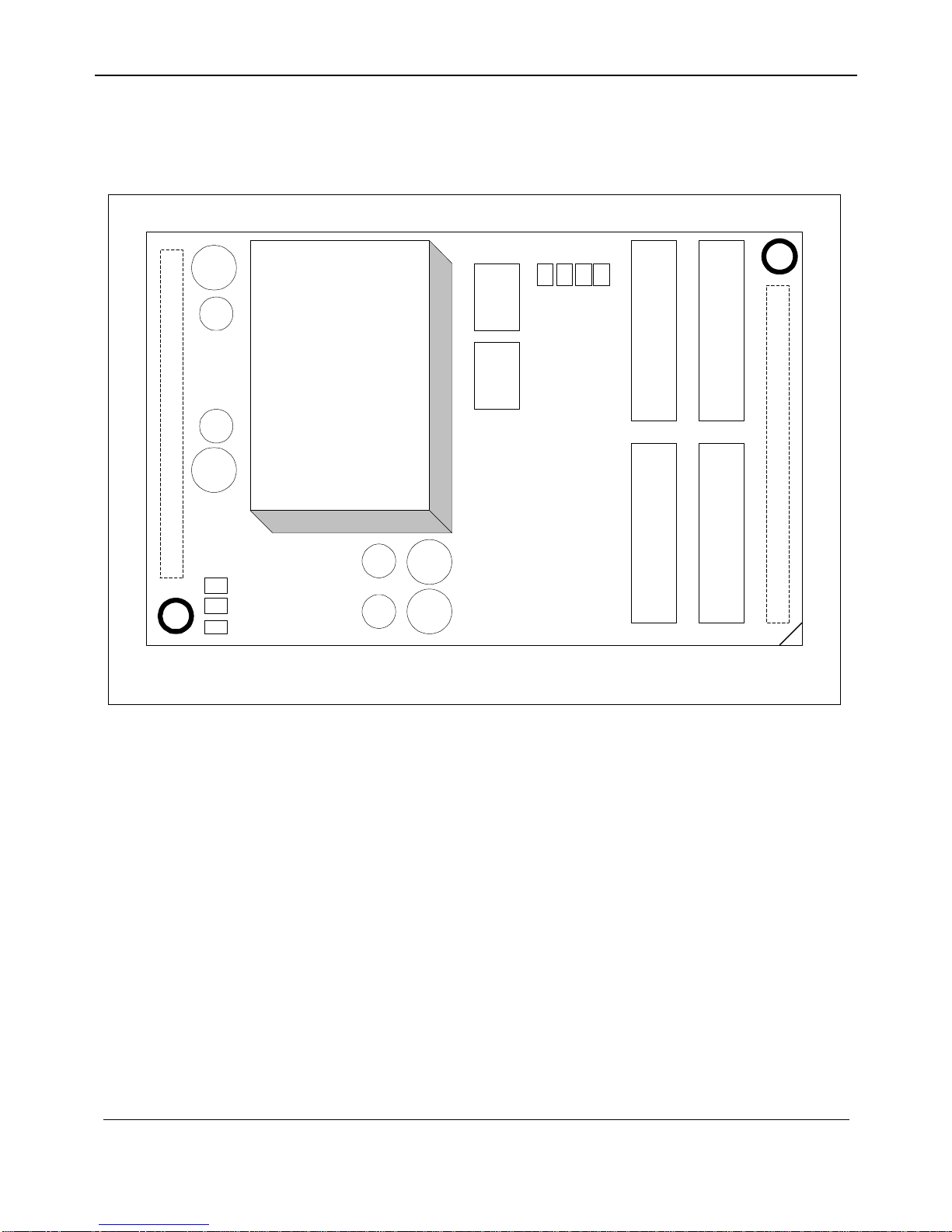
Fig. 2: Physical Layout of the SMT340/360/380
Fig. 2Shows the Physical Layout of the SMT340/360/380, indicating the external connectors with their
location and numbering. Connector definitions are as follows:
Ji1 :External clock input via 50ohm CV10 coax connector.
Ji2 :External clock input via 50ohm MMBX coax connector.
Ji3 :External enable/trigger input via 50ohm CV10 coax connector.
Ji4 :External enable/trigger input via 50ohm MMBX coax connector.
Ji5 :Channel A analogue input via 50ohm CV10 coax connector.
Ji6 :Channel A analogue input via 50ohm MMBX coax connector.
Ji7 :Channel B analogue input via 50ohm CV10 coax connector.
Ji8 :Channel B analogue input via 50ohm MMBX coax connector.
Shielded ADCs
S2
S1
P2 - Bottom Primary Connector
P1 - Top Primary Connector
SDB (Jo1)SDB (Jo3)
SDB (Jo2) (Not mounted on
SMT340 and SMT360)
SDB (Jo4) (Not mounted on
SMT340 and SMT360)
Ji7
Ji8
Ji6
Ji5
Ji2
Ji4
Ji1
Ji3
LEDS
LEDS
Rev01, Issue01
SMT340_60_80_PCB_Layout_Rev01_Iss01.vsd
D1
PD1
PD2
LD2
LD1
LD4
LD3
Note : On the SMT380-02 PCB the TIM-site is
rotated through 180 Degrees

Preliminary Page 11 of 28
Document Name: SMT340_360_380_User_Manual_Rev01_Iss01.doc Revision: 01
Document Number: TBD Original Date: 25 June 2001
Author: PC Pelser / MR Vogel Revision Date: 25 June 2001
Document Title: SMT340/360/380 User Manual
Jo1 :Primary output data path for Channel B via SDB connector (Sample T)
Jo2 :Secondary output data path for Channel B via SDB connector (Sample T + 1) This
Connector is used only on the SMT380 and is reserved on the SMT340 and the SMT360.
Jo3 :Primary output data path for Channel A via SDB connector (Sample T)
Jo4 :Secondary output data path for Channel A via SDB connector (Sample T + 1) This
Connector is used only on the SMT380 and is reserved on the SMT340 and the SMT360.
Refer to section 8 for a description of S1, S2 and the LEDs. Also refer to the TIM Specification for a
description of the Primary and Secondary TIM connectors.

Preliminary Page 12 of 28
Document Name: SMT340_360_380_User_Manual_Rev01_Iss01.doc Revision: 01
Document Number: TBD Original Date: 25 June 2001
Author: PC Pelser / MR Vogel Revision Date: 25 June 2001
Document Title: SMT340/360/380 User Manual
7. SMT380 SPECIFICATIONS
The following important specifications should be noted when using the SMT340/360/380.
Table 1: SMT340/360/380 Specifications
Description Specification
Analogue inputs (Ji5 to Ji8)
Maximum voltage 1Vp-p (+/- 500 mV)
Impedance 50Ω
Bandwidth No Bandwidth filtering is applied on the module
(Typical bandwidth for AD9432 ADC is 500 MHz)
External clock input (Ji1 or Ji2)
Maximum voltage ±2.5V
Minimum voltage ±1V
Impedance 50Ω
Frequency range 1MHz to 40MHz – SMT340
1MHz to 65MHz – SMT360
1MHz to 105MHz – SMT380
Signal format Low jitter sinusoidal or TTL
External Enable/Trigger input (Ji3 or Ji4)
Impedance 50Ω
Frequency range 0Hz to 20MHz – SMT340
0Hz to 32.5MHz – SMT360
0Hz to 52.5MHz – SMT380
Signal format TTL
SMT340/360/380 Output and Power Supply Specifications
Output Data Width 16-Bits
Significant Bits 12-Bits or 8-Bits (See section 8 for more detail)
Data Format 2’s Compliment
SFDR Typically 65 dB
SNR Typically 60 dB
Maximum Sampling Frequency over 1 SDB (SMT340
and SMT360) 40MHz – SMT340
65MHz - SMT360
Maximum Sampling Frequency over 2 SDBs
(SMT380 only) 100MHz – SMT380
(50MHz per SDB)
Power Consumption on +5V Supply 1.2 W – See Section 10
Power Consumption on +3.3V Supply 2.5 W – See Section 10
Power Consumption on –12V Supply 1.1 W – See Section 10

Preliminary Page 13 of 28
Document Name: SMT340_360_380_User_Manual_Rev01_Iss01.doc Revision: 01
Document Number: TBD Original Date: 25 June 2001
Author: PC Pelser / MR Vogel Revision Date: 25 June 2001
Document Title: SMT340/360/380 User Manual
8. CONFIGURATION
8.1 SMT340/360/360 DIP switch selectable options
The SMT340/360/380 is set-up from two DIP Switches, S1 and S2. The different options that can be
selected with these switches are shown in Table 2 and Table 3:
Table 2: SMT340/360/380 switch S1 set-up
Switch Bits Description Possible Values
S1 [2..1] Clock source selection B2
OFF
OFF
ON
ON
B1
OFF
ON
OFF
ON
Selected clock source
External clock
Onboard oscillator
External clock
Unused
S1 [4..3] Capture Mode selection B4
OFF
OFF
ON
ON
B3
OFF
ON
OFF
ON
Selected capture Mode
Disabled
Always enabled
Use External enable
Use External trigger
S1 [6..5] Output Data Format selection: B6
OFF
OFF
ON
ON
B5
OFF
ON
OFF
ON
Selected capture Mode
16-Bit over one SDB
16-bit over two SDBs - SMT380.
Reserved on SMT340 and SMT360
Packed 8-bit over one SDB
Packed 8-bit over two SDBs -
SMT380. Reserved on SMT340 and
SMT360
S1 [7] Enable/disable test value generation B7
OFF
ON
Selected data source for control FPGA
ADC data used as source
Counter values used as source
S1 [8] Enable/Disable Channel A B8
OFF
ON
Channel A
Disabled
Enabled

Preliminary Page 14 of 28
Document Name: SMT340_360_380_User_Manual_Rev01_Iss01.doc Revision: 01
Document Number: TBD Original Date: 25 June 2001
Author: PC Pelser / MR Vogel Revision Date: 25 June 2001
Document Title: SMT340/360/380 User Manual
Table 3: SMT340/360/380 switch S2 set-up
Switch Bits Description Possible Values
S2 [7..1] Number of 128-sample blocks to capture after a trigger
event. Use this switch setting to select the number of
blocks by providing the correct binary number. OFF is
a zero, ON is a one
Number
0: 0000000
1: 0000001
2: 0000010
: :
127: 111111
Number of blocks
0 blocks (0 samples)
1 block (128 samples)
2 blocks (256 samples)
: :
127 blocks (16256 samples)
S2 [8] Enable/Disable Channel B B8
OFF
ON
Channel B
Disabled
Enabled
8.1.1 Clock source selection
The user has an option of two clock sources, the onboard oscillator (40MHz – SMT340, 64MHz –
SMT360 or 105MHz – SMT380) can be used or an external clock can be provided. The external clock
should typically be correlated to the system clock and can have a frequency of 1MHz to 40MHz for the
SMT340, 1MHz to 65MHz for the SMT360 and 1MHz to 105MHz for the SMT380.
8.1.2 Capture Mode selection
The user has the option to select one of four different formats and data routing options. The intention of
these different options is to reduce the bandwidth over a specific SDB connector.
8.1.2.1 16-Bit over one SDB
In this mode the ADC data is converted to 16-bit signed data. The 16-bit data is transmitted via the
primary SDB connector (Jo3 for channel A, Jo1 for channel B) at the rate of the clock source. The
maximum frequency over a single SDB is 65 MHz.
8.1.2.2 16-bit over two SDBs (Only applicable to the SMT380)
In this mode the ADC data is converted to 16-bit signed data. The samples are then distributed between
the primary and secondary SDB connector. Each connector will now have a clock and data rate equal to
half the rate of the clock source. The primary connector will transmit all the even samples (0,2,4,6..)
while the secondary connector will transmit the odd samples (1,3,5,7..). For channel A use Jo3 (primary)
and Jo4 (secondary), for channel B use Jo1 (primary) and Jo2 (secondary).
8.1.2.3 Packed 8-bit over one SDB
In this mode the ADC data is converted to 8-bit signed data. The samples are then distributed between the
LSB eight bits and MSB eight bits before it is transmitted via one SDB connector at half rate (Jo3 for
channel A, Jo1 for channel B). The primary connector will transmit all the samples with the even samples
(0,2,4,6..) contained in the LSB eight bit and the samples (1,3,5,7..) contained in the MSB eight bits.

Preliminary Page 15 of 28
Document Name: SMT340_360_380_User_Manual_Rev01_Iss01.doc Revision: 01
Document Number: TBD Original Date: 25 June 2001
Author: PC Pelser / MR Vogel Revision Date: 25 June 2001
Document Title: SMT340/360/380 User Manual
8.1.2.4 Packed 8-bit over two SDBs (Only applicable to the SMT380)
In this mode the ADC data is converted to 8-bit signed data. The samples are then distributed between the
LSB eight bits and MSB eight bits before it is redistributed between primary and secondary SDB
connectors at a quarter of the clock rate. The primary connector will transmit the first two samples
(LSB[0],MSB[1],LSB[4],MSB[5]..), while the secondary connector will transmit the next two
(LSB[2],MSB[3],LSB[6],MSB[7]..). For channel A use Jo3 (primary) and Jo4 (secondary), for channel B
use Jo1 (primary) and Jo2 (secondary).
8.2 LED Indicators
Led: LD1 will be ON if clipping on Channel A occurs.
Led: LD3 will be ON if clipping on Channel B occurs.
Led: LD2 will be ON if test value generation for Channel A is enabled.
Led: LD4 will be ON if test value generation for Channel B is enabled.
Led: D1 will be ON if +5V is present.
Led: PD1 will be ON if +3.3V is present.
Led: PD2 will be ON if –12V is present.

Preliminary Page 16 of 28
Document Name: SMT340_360_380_User_Manual_Rev01_Iss01.doc Revision: 01
Document Number: TBD Original Date: 25 June 2001
Author: PC Pelser / MR Vogel Revision Date: 25 June 2001
Document Title: SMT340/360/380 User Manual
9. PRECAUTIONS
In order to guarantee that the SMT340/360/380 functions correctly and to protect the module from
damage the following precautions should be taken:
1. The SMT340/360/380 is a static sensitive device and should be handled accordingly. Always place
the module in a static protective bag during storage and transition.
2. When operated in a closed environment make sure that heat generated by the system is extracted, e.g.
a Fan extracting heat or blowing cool air over the modules.

Preliminary Page 17 of 28
Document Name: SMT340_360_380_User_Manual_Rev01_Iss01.doc Revision: 01
Document Number: TBD Original Date: 25 June 2001
Author: PC Pelser / MR Vogel Revision Date: 25 June 2001
Document Title: SMT340/360/380 User Manual
10. POWER SUPPLY
The SMT340/360/380 requires +5V, +3.3V, -12V for operation.
+5V is derived from the TIM connectors.
+3.3V is derived from the TIM mounting holes.
-12V is derived from the TIM connectors and is converted on-board to –5V and is used for powering the
critical analogue circuitry.

Preliminary Page 18 of 28
Document Name: SMT340_360_380_User_Manual_Rev01_Iss01.doc Revision: 01
Document Number: TBD Original Date: 25 June 2001
Author: PC Pelser / MR Vogel Revision Date: 25 June 2001
Document Title: SMT340/360/380 User Manual
11. DEMONSTRATION SOFTWARE
The SMT340/360/380 is shipped with a Test program (Executable and source code) for the SMT332 C6x
TIM, which demonstrates the use of SMT340/360/380 with an SMT332 to capture a high bandwidth
analogue signal. The following files are included (x is 4 for the SMT340, 6 for the SMT360 and 8 for the
SMT380):
1. Program files:
SMT3x0.C
SMT3x0.CMD
SMT332.H
SMT332LIB.C
2. SMT340/360/380 Captured Data Text File:
SMT3x0.DAT
3. Matlab command files for analysis of captured data:
SMT3x0.M
WINDOW512.MAT
WINDOW.MAT
WINDOW2.MAT
WINDOW4.MAT
WINDOW8.MAT

Preliminary Page 19 of 28
Document Name: SMT340_360_380_User_Manual_Rev01_Iss01.doc Revision: 01
Document Number: TBD Original Date: 25 June 2001
Author: PC Pelser / MR Vogel Revision Date: 25 June 2001
Document Title: SMT340/360/380 User Manual
12. APPENDIX A : SAMPLE DATA
12.1 SMT340 Sample Plots
Fig. 3: Full scale 1.4MHz filtered input signal sampled at 40MHz

Preliminary Page 20 of 28
Document Name: SMT340_360_380_User_Manual_Rev01_Iss01.doc Revision: 01
Document Number: TBD Original Date: 25 June 2001
Author: PC Pelser / MR Vogel Revision Date: 25 June 2001
Document Title: SMT340/360/380 User Manual
12.2 SMT360 Sample Plots
Fig. 4: Full scale 1.4MHz filtered input signal sampled at 65MHz
Fig. 5: Full scale 15MHz unfiltered input signal sampled at 65MHz
This manual suits for next models
2
Table of contents