AXIOMTEK AX93285 User manual
Other AXIOMTEK Control Unit manuals
AXIOMTEK
AXIOMTEK AX93262 User manual
AXIOMTEK
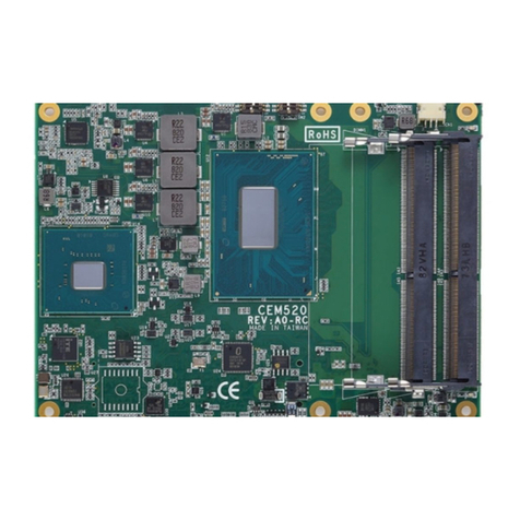
AXIOMTEK CEM520 User manual
AXIOMTEK
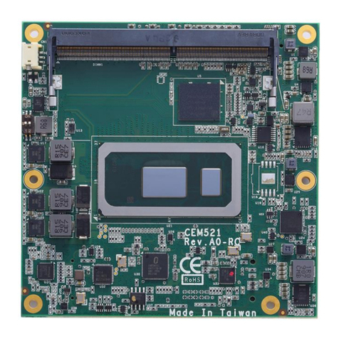
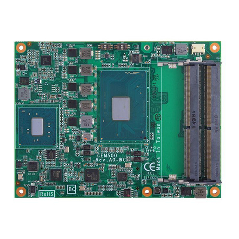
AXIOMTEK CEM521 User manual
AXIOMTEK
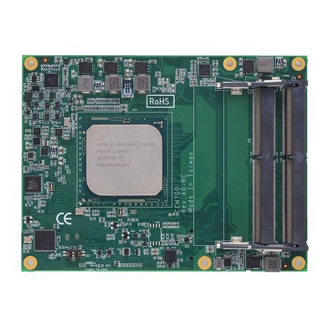
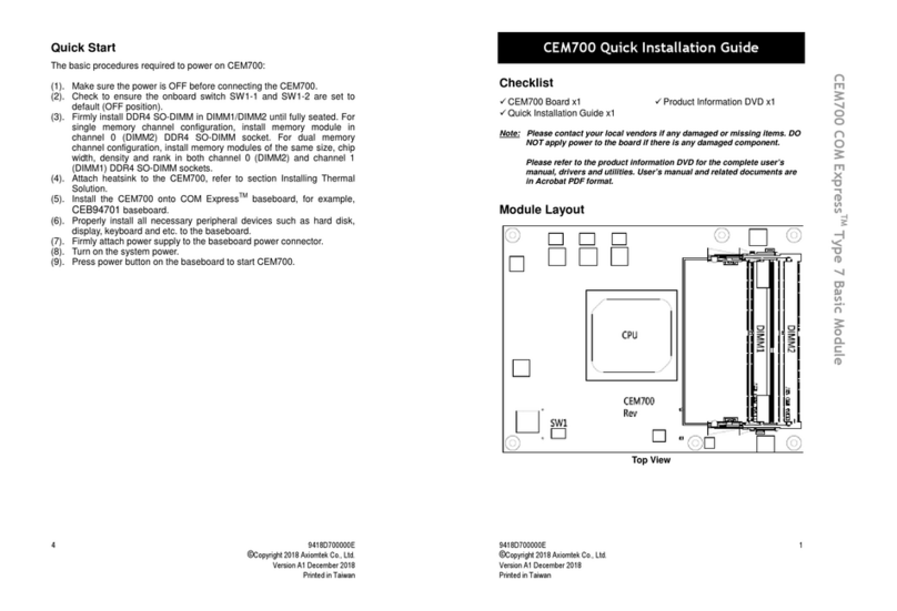
AXIOMTEK CEM700 User manual
AXIOMTEK
AXIOMTEK CEM510 User manual

AXIOMTEK
AXIOMTEK SDM300S User manual

AXIOMTEK
AXIOMTEK SDM500L User manual
AXIOMTEK
AXIOMTEK AX12270 User manual
AXIOMTEK
AXIOMTEK AX93304 User manual
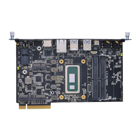
AXIOMTEK
AXIOMTEK SDM500L User manual
AXIOMTEK
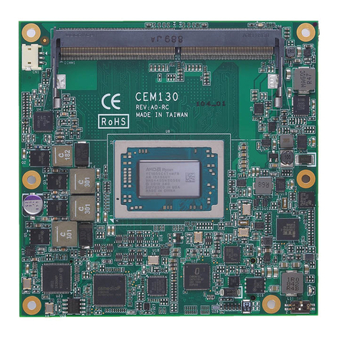
AXIOMTEK CEM130 User manual
AXIOMTEK
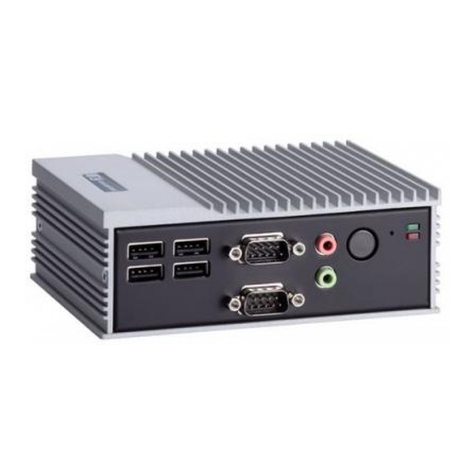
AXIOMTEK eBOX530-830-FL User manual
AXIOMTEK
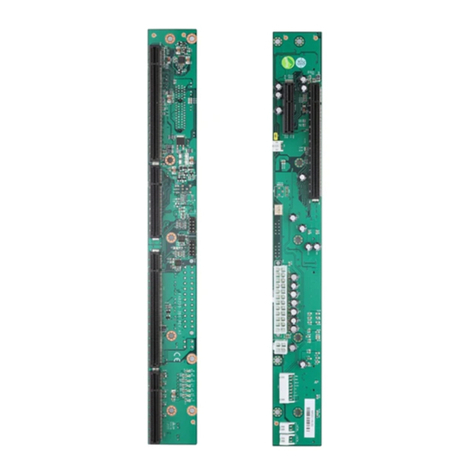
AXIOMTEK FAB209-3B1 User manual
AXIOMTEK
AXIOMTEK STX88810VEA User manual
AXIOMTEK
AXIOMTEK FAB205-6P5 Series User manual

AXIOMTEK
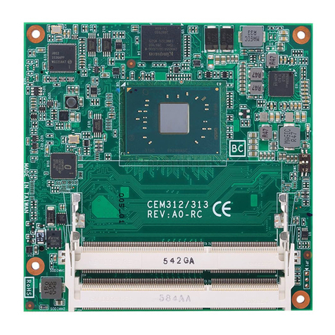
AXIOMTEK CEM313 User manual
AXIOMTEK
AXIOMTEK CEM312 User manual
AXIOMTEK
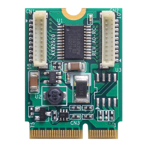
AXIOMTEK AX92920 User manual
AXIOMTEK
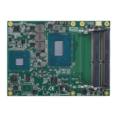
AXIOMTEK CEM530 User manual
AXIOMTEK
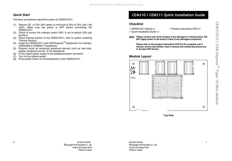
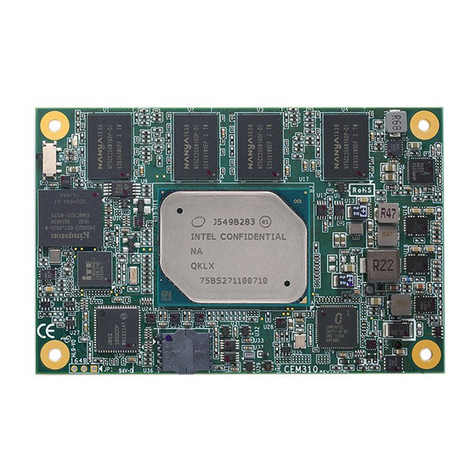
AXIOMTEK CEM310 User manual
Popular Control Unit manuals by other brands
Festo
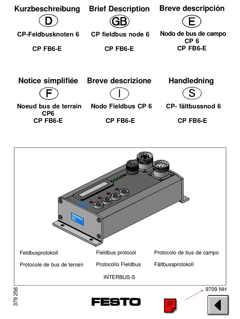
Festo Compact Performance CP-FB6-E Brief description
Elo TouchSystems
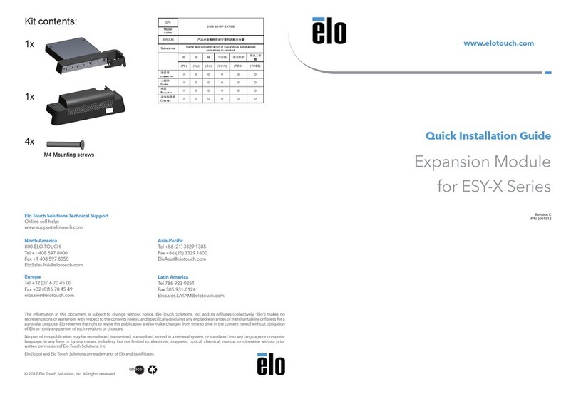
Elo TouchSystems DMS-SA19P-EXTME Quick installation guide
JS Automation
JS Automation MPC3034A user manual
JAUDT
JAUDT SW GII 6406 Series Translation of the original operating instructions
Spektrum
Spektrum Air Module System manual
BOC Edwards
BOC Edwards Q Series instruction manual

KHADAS
KHADAS BT Magic quick start
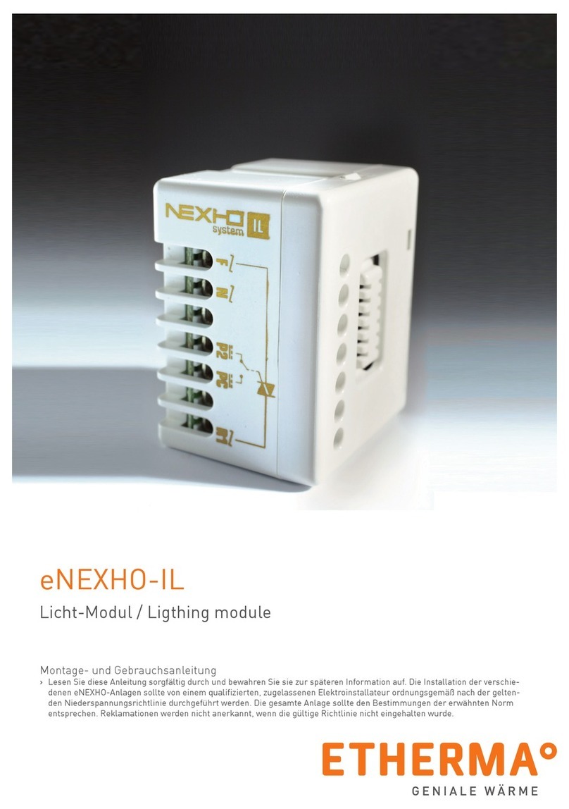
Etherma
Etherma eNEXHO-IL Assembly and operating instructions
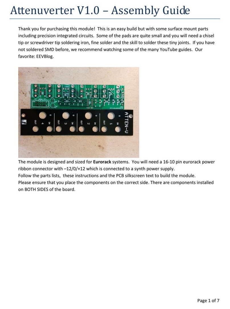
PMFoundations
PMFoundations Attenuverter Assembly guide
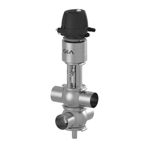
GEA
GEA VARIVENT Operating instruction
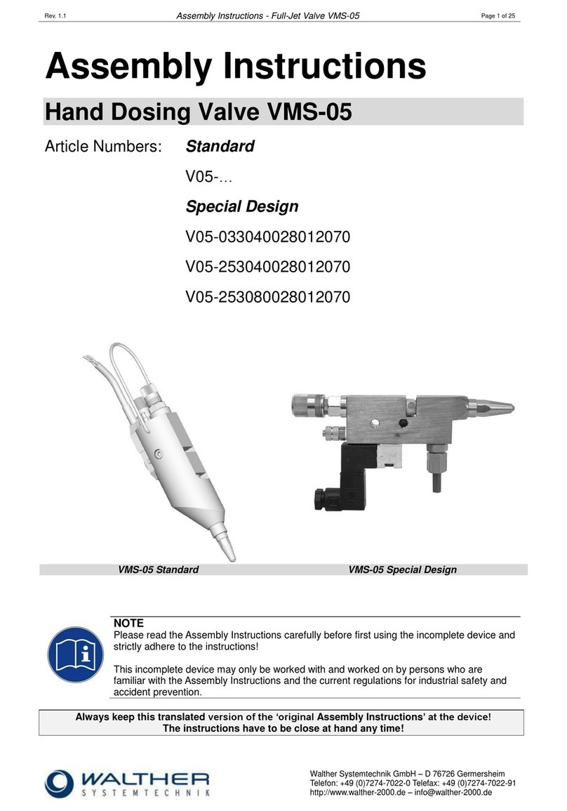
Walther Systemtechnik
Walther Systemtechnik VMS-05 Assembly instructions
Altronix
Altronix LINQ8PD Installation and programming manual
