Pentek Model 7341 Installation Manual Page 3
Page
Table of Contents
Rev.: B
Chapter 1: Introduction
1.1 General Des ription..............................................................................................................................5
1.2 Features ..................................................................................................................................................5
1.3 Model 7341 Do umentation ................................................................................................................5
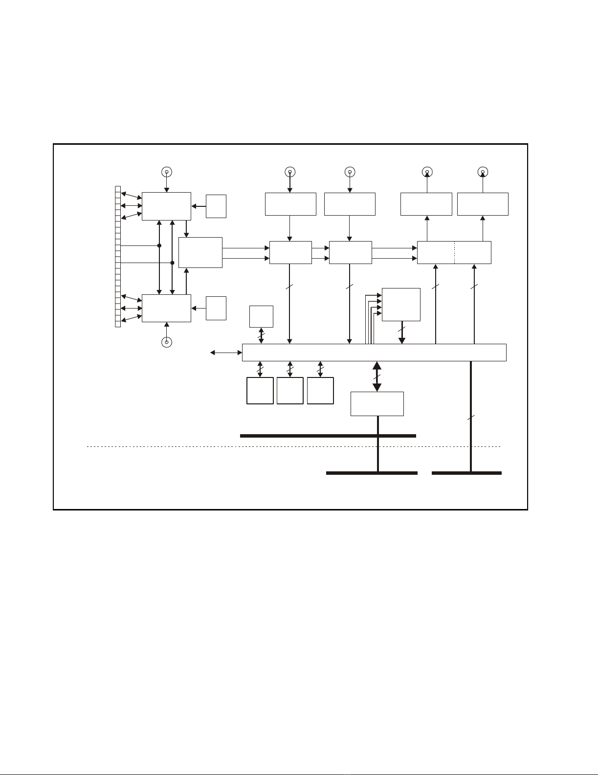
1.4 Blo k Diagram.......................................................................................................................................6
igure 1−1: Model 7341 Block Diagram...........................................................................................6
1.5 Prin iple of Operation..........................................................................................................................7
1.6 Spe ifi ations.........................................................................................................................................8
Chapter 2: Installation and Connections
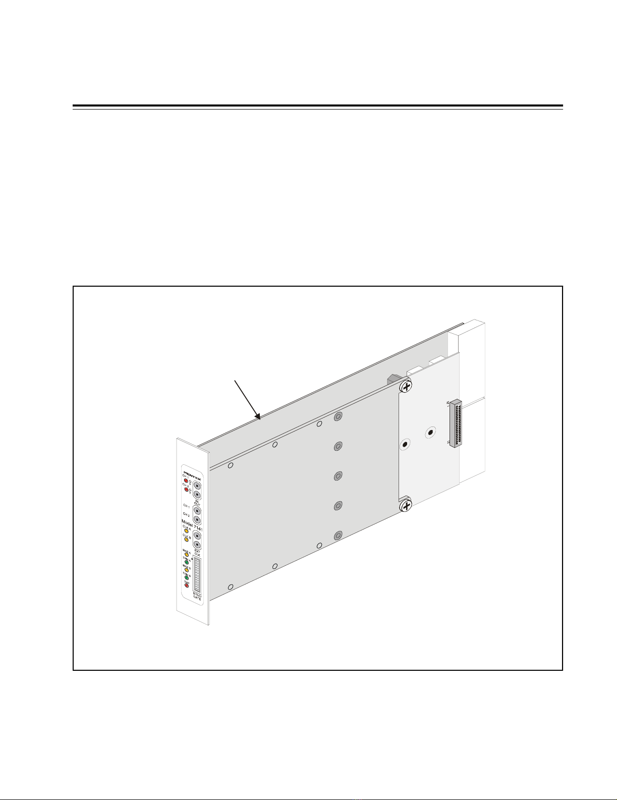
2.1 Inspe tion...............................................................................................................................................9
igure 2−1: Model 7341 Assembly....................................................................................................9
2.2 Jumper Settings...................................................................................................................................10
igure 2−2: PMC to cPCI Carrier, PMC Connection Side..........................................................11
2.2.1 Removing PMC Module from PCI Carrier .................................................................12
igure 2−3: Removing PMC Module from cPCI Carrier...........................................12
2.2.2 Removing PMC Module from PCI Carrier − Condu tion Cooled ..........................13
igure 2−4: Model 7141−703 PMC Mounting..............................................................13
2.2.3 Repla ing PMC Module onto PCI Carrier ...................................................................14
igure 2−5: cPCI Carrier PMC Connections ................................................................14
2.2.4 Repla ing PMC Module onto PCI Carrier − Condu tion Cooled ...........................15
igure 2−6: cPCI Carrier PMC Connections ................................................................15
2.3 7141 PMC Module Jumpers ..............................................................................................................16
igure 2−7: 7141 PMC Module, Component Side .......................................................................16
Table 2−1: Jumper Blocks JB1 & JB2..............................................................................................16
2.4 Installing the Model 7341 in a PCI Card Cage..............................................................................17
2.5 FPGA I/O Conne tions (Option 104) ..............................................................................................18
Table 2−2: Option 104 PGA I/O Pin Connections.....................................................................19
2.6 Front Panel Conne tions....................................................................................................................20
igure 2−8: 7141 PMC ront Panel.................................................................................................20
2.6.1 Analog Input Conne tors ................................................................................................20
2.6.2 Analog Output Conne tors .............................................................................................20
2.6.3 Clo k Input Conne tors ...................................................................................................20
2.6.4 SYNC/GATE Conne tor .................................................................................................21
Table 2−3: SYNC/GATE Connector Pins .....................................................................21
2.7 Front Panel LEDs................................................................................................................................22
2.7.1 Overload LEDs ..................................................................................................................22
2.7.2 Clo k LEDs ........................................................................................................................22
2.7.3 Master LEDs ......................................................................................................................22
2.7.4 Terminate LEDs ................................................................................................................22
2.7.5 Over Temperature LED ...................................................................................................22