Pentium 5VD2 Use and care manual

Pentium
82430 VX/P54C PCI Mainboard
User’s Guide &
Technical Reference
5VD2/D5

ii
®
™
About This Guide
This UserÕs Guide is for assisting system manufacturers and end users in setting
up and installing the mainboard. Information in this guide has been carefully
checked for reliability; however, no guarantee is given as to the correctness of the
contents. The information in this document is subject to change without notice.
Copyright Notice
Copyright 1997, Soyo Computer Inc. All rights reserved. This manual is
copyrighted by Soyo Computer Inc. You may not reproduce, transmit, transcribe,
store in a retrieval system, or translate into any language, in any form or by any
means, electronic, mechanical, magnetic, optical, chemical, manual, or otherwise,
any part of this publication without express written permission of Soyo Computer
Inc.
Trademarks
Soyo is a registered trademark of Soyo Computer Inc. All trademarks are the
property of their owners.
Disclaimer
Soyo Computer Inc. makes no representations or warranties regarding the
contents of this manual. We reserve the right to revise the manual or make
changes in the specifications of the product described within it at any time
without notice and without obligation to notify any person of such revision or
change. The information contained in this manual is provided for general use by
our customers. Our customers should be aware that the personal computer field is
the subject of many patents. Our customers should ensure that they take
appropriate action so that their use of our products does not infringe upon any
patents. It is the policy of Soyo Computer Inc. to respect the valid patent rights of
third parties and not to infringe upon or assist others to infringe upon such rights.
Restricted Rights Legend
Use, duplication, or disclosure by the Government is subject to restrictions set
forth in subparagraph (c)(1)(ii) of the Rights in Technical Data and Computer
Software clause at 252.277-7013.
Product Rights
Product mentioned in this manual are mentioned for identification purpose only.
Product names appearing in this manual may or may not be registered trademarks
or copyrights of their respective companies.
If you need any further information, please come to our home page on internet.
The address is Òhttp://www.soyo.com.twÓ.
Edition: April 1997
Version 1.1
5VD2/D5 SERIAL

Table of Contents
Chapter 1: Introduction .................................................. 1
Key Features ............................................................................... 1
Unpacking the Mainboard........................................................... 2
Electrostatic Discharge Precautions............................................ 2
Mainboard Layout w/ Default Settings ....................................... 3
Chapter 2: Hardware Setup ............................................ 5
Jumpers ....................................................................................... 5
JP5: CMOS Clear Jumper ..................................................... 5
JPS2: PS/2 Mouse Function Jumper ..................................... 5
JP43: CPU Cooling Fan Connector...................................... 6
CPU Type Configuration ............................................................ 7
Step 1: Frequency Setting..................................................... 7
Pentium Ð 75/90/100 CPU Settings (1.5 x clock)............. 7
Pentium Ð 100/120/133 CPU Settings (2.0 x clock)......... 8
Pentium/AMD Ð 150/166 CPU Settings (2.5 x clock) ..... 9
Pentium Ð 180/200 CPU Settings (3.0 x clock)................ 9
Pentium Ð 233 CPU Settings (3.5 x clock) ..................... 10
Cyrix 6x86 Ð PR200+ CPU Settings (2.0 x clock) ......... 10
Step 2: CPU Single/Dual Voltage Setting.......................... 11
Single Voltage CPU Setting ........................................... 11
Dual Voltage CPU Setting.............................................. 12
Memory Configuration ............................................................. 13
RAM Bank Installation Notice............................................ 13
Cache Configuration ................................................................. 13
Cache Size and RAM Locations ......................................... 13
Multi I/O Port Addresses .......................................................... 14
Connectors ................................................................................ 14
COM1, COM2Ð COM1/COM2 Connectors ....................... 14
FDC Connector ................................................................... 14
J19 Ð Hardware Reset Control............................................. 14
J24 Ð HDD LED Connectors ............................................... 14
IDE1/IDE2 Ð On-board Primary/Secondary IDE HDD
Connectors ........................................................................... 15
IR1 Ð IR Connector ............................................................. 15
J2 Ð Keyboard Connector .................................................... 15
J17 Ð Keylock & Power LED Connector ............................ 15
J1 Ð PS/2 Mouse Connector ................................................ 15
PRT Ð Parallel Port Connector ............................................ 15
PW Ð Power Supply Connector ........................................... 15
J23: Sleep Switch Connector Enable/Disable ..................... 16

Connectors (Continued)
J22 Ð Turbo LED Connector ............................................... 16
USB1 Ð Universal Serial Bus Connectors ........................... 16
Chapter 3: BIOS Setup.................................................. 17
Standard CMOS Setup .............................................................. 18
BIOS Features Setup ................................................................. 20
Chipset Features Setup.............................................................. 23
Power Management Setup ........................................................ 26
PNP/PCI Configuration Setup .................................................. 28
Load Setup Defaults.................................................................. 30
Load BIOS Defaults.................................................................. 30
Integrated Peripherals ............................................................... 31
Supervisor Password ................................................................. 33
User Password ........................................................................... 34
IDE HDD Auto Detection ......................................................... 35
Chapter 4: Drivers Installation Guide ......................... 36
IDE BUS Master Installation Guide ......................................... 36
MS-DOS/WINDOW/WFW ................................................ 36
WINDOWS NT3.5/4.0........................................................ 36
WINDOWS 95 .................................................................... 37
NOVELL 3.X&4.X ............................................................. 37
SCO UNIX .......................................................................... 37
SCO UNIX 5.0 .................................................................... 38
OS/2 2.0 and WARP 3.X..................................................... 39

1 Introduction
The 82430 VX PCI mainboard is a high-performance AT form-factor
system board that supports P54C/P55C family CPUs. You can order
256K or 512K of external cache memory on the mainboard. The
mainboard is fully compatible with industry standards, and adds many
technical enhancements.
Key Features
¥ CPU
Ñ Supports P54C/P55C family CPUs running at 75~233 MHz
speeds; Cyrix 6x86/6x86L CPUs running at
PR133+/PR150+/PR166+speeds; and AMD K5/K6 CPUs
running at PR75 ~ PR266 speeds
ÑSupports SOCKET 7 for upgrade
Ñ Supports P54C/P55C series SMM Mode and CPU Stop Clock
¥ L2 Cache Controller
Ñ Write Back Cache Modes and Direct Mapped Organization
Ñ On-board 256K/512K Pipeline Burst SRAMs Cache
¥ DRAM Controller
Ñ Supports Fast-Page Mode, and EDO DRAM (both symmetrical
and asymmetrical addressing)
Ñ Supports 2 strips of 8MB/16MB/32MB Unbuffered DIMMs
Ñ On-board memory configurations from 4 to 128 Mbytes
Ñ Supports ÒTable-FreeÓ DRAM configuration in any SIMM bank
¥ BUS Controller
Ñ Compliant to PCI specifications v2.1
Ñ Four 32-bit PCI slots (Masters) and four ISA slots, 4-layer PCB
ÑSupports Universal Serial Bus Ñ USB
¥ Peripheral Controller
Ñ System BIOS built-in NCR306 SCSI Card BIOS and ÒPlug and
PlayÓ function
Ñ On-board built-in PCI Master IDE controller and floppy controller
Ñ On-board supports for two high speed UARTS (w/i 16550 FIFO),
one ECP/EPP/SPP compatible parallel port, and one PS/2 mouse
port
Ñ On-board supports FLASH Memory for easy upgrade BIOS
Ñ Easy installation of Triones EIDE/ATAPI CD-ROM Bus
Master Drivers

2Introduction
Unpacking the Mainboard
The mainboard package contains:
¥ The 82430VX Mainboard
¥ This UserÕs Guide
¥ One IDE Bus Master driver
Note: Do not unpack the mainboard until you are ready to install it.
Follow the precautions below while unpacking the mainboard.
1. Before handling the mainboard, ground yourself by grasping an
unpainted portion of the systemÕs metal chassis.
2. Remove the mainboard from its anti-static packaging and place it on
a grounded surface, component side up.
3. Check the mainboard for damage. If any chip appears loose, press
carefully to seat it firmly in its socket.
Do not apply power if the mainboard appears damaged. If there is
damage to the board contact your dealer immediately.
Electrostatic Discharge Precautions
Make sure you ground yourself before handling the mainboard or other
system components. Electrostatic discharge can easily damage the
components. Note that you must take special precaution when handling
the mainboard in dry or air-conditioned environments.
Take these precautions to protect your equipment from electrostatic
discharge:
¥ Do not remove the anti-static packaging until you are ready to install
the mainboard and other system components.
¥ Ground yourself before removing any system component from its
protective anti-static packaging. To ground yourself grasp the
expansion slot covers or other unpainted portions of the computer
chassis.
¥ Frequently ground yourself while working, or use a grounding strap.
¥ Handle the mainboard by the edges and avoid touching its
components.

Introduction 3
Mainboard Layout w/ Default Settings
2
2
2
3 3
1
5
4
4
17 16
7810
9
13
12
14 14 15
11
6
2
Figure 1Ð1. Mainboard Layout
1. ZIF socket 7 (for P54C/P55C) 10. SIMM Bank
2. 82430 VX Chipset 11. Floppy Connector
3. Pipelined Burst SRAM 12. IDE1/IDE2 Connector
4. Ultra I/O Chip 13. Parallel Port Connector
5. PnP FLASH BIOS 14. COM1/COM2 Connector
6. TAG SRAM 15. AT Power Connector
7. ISA Slots 16. KB Connector
8. PCI Slots 17. PS/2 Mouse Connector
9. Unbuffered DIMM Bank

4Introduction
Default settings are as follows: Pentium 133MHz (P54C) CPU, 256K
Pipelined Burst cache, On-board PCI E-IDE Enabled, 2 high speed
UARTS Enabled (w/ 16550 FIFO), 1 EPP/ECP port (ECP + EPP mode),
and 5V DRAM/3.3V DIMM.
82438VX
DIMM 1 (Share BANK 1)
DIMM 2 (Share BANK 0)
#4 #3 #2 #1
ISA SLOT
#1#2#3#4
PCI SLOT
SIMM BANK 0
SIMM BANK 1
82371 SB
RSTSMI
J19J24 J23
HD
LED
J18 J17
TB
LED
J22 BF2
KeylockSPK
8680
82438VX
P.B. SRAM
32Kx32
P.B. SRAM
32Kx32
J1 J2
PW
JP43
FDC
PRT
IDE 1
IDE 2
TAG SRAM
586
CPU
Family
54321
SW1
ON
Flash BIOS
USB
8687
COM2 COM1
1
IR
1
JP5
JPS2
JP301
10
82437 VX
Figure 1Ð2. Mainboard Default Setting
Important: Make sure the system is well ventilated to prevent
overheating and ensure system stability.
2 Hardware Setup
This chapter explains how to configure the mainboardÕs hardware. After
you install the mainboard, you can set jumpers, install memory on the
mainboard, and make case connections. Refer to this chapter whenever
you upgrade or reconfigure your system.
CAUTION:Turn off power to the mainboard, system chassis, and
peripheral devices before performing any work on the
mainboard or system.
Jumpers
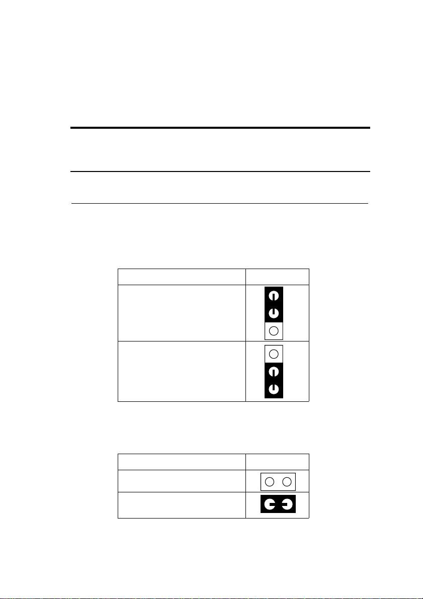
JP5: CMOS Clear Jumper
Clear the CMOS memory by momentarily shorting pin 2Ð3; then
shorting pin 1Ð2 to retain new settings.
CMOS Setting JP5
Retain CMOS data
(default)
1
Clear CMOS data
1
JPS2: PS/2 Mouse Function Jumper
Set PS/2 mouse function enabled or disabled.
PS/2 Mouse Function JPS2
Disabled
Enabled
(default)
Note: The IRQ12 is dedicated to the PS/2 mouse when choosing
enabled of PS/2 Mouse Function.

6Hardware Setup
JP43: CPU Cooling Fan Connector
This 3-pins connector provides 12V power for the CPU cooling fan
which matches the pin assignment of this connector.
CPU Cooling Fan Connector
(Pin Assignment)
1 (GND)
2 (12V)
3 (GND)
Note: Make sure the pin assignment is matched with this connector
before connecting it, otherwise, you may damage either the
mainboard or the cooling fan.
This manual suits for next models
1
Table of contents
Other Pentium Motherboard manuals

Pentium
Pentium 5VC2 Use and care manual

Pentium
Pentium P51437P4/FMB User manual

Pentium
Pentium GA - 586IP User manual

Pentium
Pentium IN530 User manual

Pentium
Pentium P5V580 VP3 Advance II User manual

Pentium
Pentium P51430VX-280DM Explorer III User manual

Pentium
Pentium GA - 586ATV User manual

Pentium
Pentium P55-IT User manual

Pentium
Pentium P51430TX-250 User manual

Pentium
Pentium 5VM2 Use and care manual


