Pentium 82430 VX/P54C Use and care manual

Pentium
82430 VX/P54C PCI Mainboard
User’s Guide &
Technical Reference
5VM2/M5

ii
®
™
About This Guide
This UserÕs Guide is for assisting system manufacturers and end users in setting
up and installing the mainboard. Information in this guide has been carefully
checked for reliability; however, no guarantee is given as to the correctness of the
contents. The information in this document is subject to change without notice.
Copyright Notice
Copyright 1996, Soyo Computer Inc. All rights reserved. This manual is
copyrighted by Soyo Computer Inc. You may not reproduce, transmit, transcribe,
store in a retrieval system, or translate into any language, in any form or by any
means, electronic, mechanical, magnetic, optical, chemical, manual, or otherwise,
any part of this publication without express written permission of Soyo Computer
Inc.
Trademarks
Soyo is a registered trademark of Soyo Computer Inc. All trademarks are the
property of their owners.
Disclaimer
Soyo Computer Inc. makes no representations or warranties regarding the
contents of this manual. We reserve the right to revise the manual or make
changes in the specifications of the product described within it at any time
without notice and without obligation to notify any person of such revision or
change. The information contained in this manual is provided for general use by
our customers. Our customers should be aware that the personal computer field is
the subject of many patents. Our customers should ensure that they take
appropriate action so that their use of our products does not infringe upon any
patents. It is the policy of Soyo Computer Inc. to respect the valid patent rights of
third parties and not to infringe upon or assist others to infringe upon such rights.
Restricted Rights Legend
Use, duplication, or disclosure by the Government is subject to restrictions set
forth in subparagraph (c)(1)(ii) of the Rights in Technical Data and Computer
Software clause at 252.277-7013.
Product Rights
Product mentioned in this manual are mentioned for identification purpose only.
Product names appearing in this manual may or may not be registered trademarks
or copyrights of their respective companies.
If you need any further information, please come to our home page on internet.
The address is Òhttp://www.soyo.com.twÓ.
Edition: March 1997
Version 1.0
5VM2/M5 SERIAL

Table of Contents
Chapter 1: Introduction .................................................. 1
Key Features ............................................................................... 1
Unpacking the Mainboard........................................................... 2
Electrostatic Discharge Precautions............................................ 2
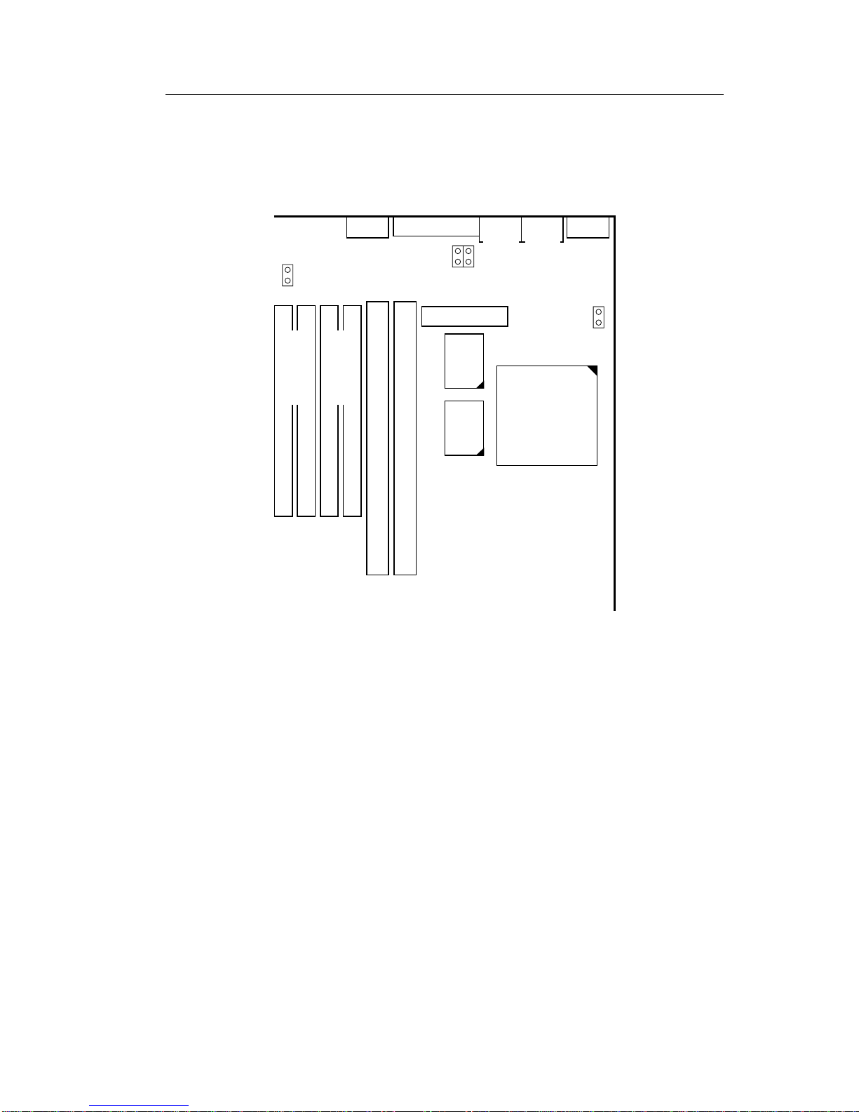
Mainboard Layout w/ Default Settings ....................................... 3
Chapter 2: Hardware Setup ............................................ 5
Jumpers ....................................................................................... 5
JP5: CMOS Clear Jumper ..................................................... 5
EMI1/EMI2/EMI3 (JP52/EMIGND/JP53): EMI Ground
Jumper ................................................................................... 6
CPU Type Configuration ............................................................ 7
Step 1: Frequency Setting..................................................... 7
Pentium Ð 75/90/100 CPU Settings (1.5 x clock)............. 7
Pentium Ð 100/120/133 CPU Settings (2.0 x clock)......... 8
PentiumÐ 150/166 CPU Settings (2.5 x clock) ................. 9
Pentium Ð 180/200 CPU Settings (3.0 x clock)................ 9
Step 2: CPU Single/Dual Voltage Setting.......................... 10
Single Voltage CPU Setting ........................................... 10
Dual Voltage CPU Setting.............................................. 11
Memory Configuration ............................................................. 12
Memory Configuration Table.............................................. 12
RAM Bank Installation Notice............................................ 12
Cache Configuration ................................................................. 13
Cache Size and RAM Locations ......................................... 13
Multi I/O Port Addresses .......................................................... 13
Connectors ................................................................................ 14
ATX PW Ñ ATX Power Supply Connectors ..................... 14
COM1, COM2Ð COM1/COM2 Connectors ....................... 14
FDC Connector ................................................................... 14
JP51 Ñ Force Power Down Jumper (Optional).................. 14
J19 Ð Hardware Reset Control............................................. 14
J24 Ð HDD LED Connectors ............................................... 15
IDE1/IDE2 Ð On-board Primary/Secondary IDE HDD
Connectors ........................................................................... 15
CN5 Ð IR Connector............................................................ 15
CN2 Ð PS/2 Keyboard Connector ....................................... 15
J17 Ð Keylock & Power LED Connector ............................ 15
LED1 Ñ ATX Power Supply Indication LED ................... 15
CN1 Ð PS/2 Mouse Connector ............................................ 15
PRT Ð Parallel Port Connector ............................................ 15

JP50 (PW2) Ñ ATX Power Supply On/Off Switch Connector
............................................................................................. 15
J23: Sleep Switch Connector Enable/Disable ..................... 16
J18 Ñ Speaker Connector ................................................... 16
J22 Ð Turbo LED Connector ............................................... 16
CN4 Ð Universal Serial Bus Connectors ............................. 16
Chapter 3: BIOS Setup.................................................. 17
Standard CMOS Setup .............................................................. 18
BIOS Features Setup ................................................................. 20
Chipset Features Setup.............................................................. 23
Power Management Setup ........................................................ 26
PNP/PCI Configuration Setup .................................................. 28
Load Setup Defaults.................................................................. 30
Load BIOS Defaults.................................................................. 30
Integrated Peripherals ............................................................... 31
Supervisor Password ................................................................. 34
User Password ........................................................................... 35
IDE HDD Auto Detection ......................................................... 36
Chapter 4: Drivers Installation Guide ......................... 37
IDE BUS Master Installation Guide ......................................... 37
MS-DOS/WINDOW/WFW ................................................ 37
WINDOWS NT3.5 .............................................................. 37
WINDOWS 95 .................................................................... 38
NOVELL 3.X&4.X ............................................................. 38
SCO UNIX .......................................................................... 38
SCO UNIX 5.0 .................................................................... 39
OS/2 2.0 and WARP 3.X..................................................... 40

1 Introduction
The 82430 VX PCI mainboard is a high-performance ATX form-factor
system board that supports P54C/P55C family CPUs. You can order
256K or 512K of external cache memory on the mainboard. The
mainboard is fully compatible with industry standards, and adds many
technical enhancements.
Key Features
¥ CPU
Ñ Supports P54C/P55C family CPUs running at 75~200 MHz
speeds; Cyrix 6x86/6x86L CPUs running at P133+/P150+/P166+
MHz speeds; and AMD K5 CPUs.
ÑSupports SOCKET 7 for upgrade
Ñ Supports P54CX/P55CX SMM Mode and CPU Stop Clock
¥ L2 Cache Controller
Ñ Write Back Cache Modes and Direct Mapped Organization
Ñ On-board 256K/512K Pipeline Burst SRAMs Cache
¥ DRAM Controller
Ñ Supports Fast-Page Mode, EDO , and SDRAM (both symmetrical
and asymmetrical addressing)
Ñ Supports 2 strips of 8MB/16MB/32MB Unbuffered DIMMs
Ñ On-board memory configurations from 4 to 128 Mbytes
Ñ Supports ÒTable-FreeÓ DRAM configuration in any SIMM bank
¥ BUS Controller
Ñ Compliant to PCI specifications v2.1
Ñ Four 32-bit PCI slots (Masters) and three ISA slots, 4-layer PCB
ÑSupports Universal Serial Bus Ñ USB
¥ Peripheral Controller
Ñ System BIOS built-in NCR810 SCSI Card BIOS, SY-S8115 SCSI
Card BIOS, SY-V325-2M VGA Card BIOS, and ÒPlug and PlayÓ
function
Ñ On-board built-in PCI Master IDE controller and floppy controller
Ñ On-board supports for two high speed UARTS (w/i 16550 FIFO),
one ECP/EPP/SPP compatible parallel port, and one PS/2 mouse
port
Ñ On-board supports FLASH Memory for easy upgrade BIOS
Ñ Easy installation of Triones EIDE/ATAPI CD-ROM Bus
Master Drivers

2Introduction
Unpacking the Mainboard
The mainboard package contains:
¥ The 82430VX Mainboard
¥ This UserÕs Guide
¥ One IDE Bus Master driver diskette
Note: Do not unpack the mainboard until you are ready to install it.
Follow the precautions below while unpacking the mainboard.
1. Before handling the mainboard, ground yourself by grasping an
unpainted portion of the systemÕs metal chassis.
2. Remove the mainboard from its anti-static packaging and place it on
a grounded surface, component side up.
3. Check the mainboard for damage. If any chip appears loose, press
carefully to seat it firmly in its socket.
Do not apply power if the mainboard appears damaged. If there is
damage to the board contact your dealer immediately.
Electrostatic Discharge Precautions
Make sure you ground yourself before handling the mainboard or other
system components. Electrostatic discharge can easily damage the
components. Note that you must take special precaution when handling
the mainboard in dry or air-conditioned environments.
Take these precautions to protect your equipment from electrostatic
discharge:
¥ Do not remove the anti-static packaging until you are ready to install
the mainboard and other system components.
¥ Ground yourself before removing any system component from its
protective anti-static packaging. To ground yourself grasp the
expansion slot covers or other unpainted portions of the computer
chassis.
¥ Frequently ground yourself while working, or use a grounding strap.
¥ Handle the mainboard by the edges and avoid touching its
components.

Introduction 3
Mainboard Layout w/ Default Settings
1
7
4
89
10
2
2
2
3
3
2
5
11
12
14 14
13 17 16
15
6
Figure 1Ð1. Mainboard Layout
1. ZIF socket 7 (for P54C/P55C) 10. Unbuffered DIMM Bank
2. 82430 VX Chipset 11. Floppy Connector
3. Pipelined Burst SRAM 12. IDE1/IDE2 Connector
4. Ultra I/O Chip 13. Parallel Port Connector
5. PnP FLASH BIOS 14. COM1/COM2 Connector
6. TAG SRAM 15. ATX Power Connector
7. ISA Slots 16. PS/2 Mouse Connector
8. PCI Slots 17. PS/2 KB Connector
9. SIMM Bank

4Introduction
Default settings are as follows: Pentium 100MHz (P54C) CPU, 256K
Pipelined Burst cache, On-board PCI E-IDE Enabled, 2 high speed
UARTS Enabled (w/ 16550 FIFO), 1 EPP/ECP port (ECP + EPP mode),
and 5V DRAM/3.3V DIMM.
#3 #2 #1
ISA SLOT
#2#3#4
PCI SLOT
SIMM BANK 0
SIMM BANK 1
82371 SB
82437 VX
JP5
COM1COM2
#1
ALI
5143
82438VX82438VX
P.B. SRAM
32Kx32
P.B. SRAM
32Kx32
PRT
FDC
IDE 1
IDE 2
TAG SRAM
586
CPU
Family
Flash BIOS
USB CN4
EMI1
EMI3
12345
SW1
ON
1
CN5
IR
1
JP30
DIMM1 (Share Bank 0)
DIMM2 (Share Bank 1)
PS/2
KB
Conn.
ATX PW
EMI2
JP31
1357
1
J17
1
J18 J22 J19 J23 J24
PW2
Keylock Speaker TB
LED RST HD
LED
PS/2
Mouse
Conn.
Figure 1Ð2. Mainboard Default Setting
Important: Make sure the system is well ventilated to prevent
overheating and ensure system stability.

2 Hardware Setup
This chapter explains how to configure the mainboardÕs hardware. After
you install the mainboard, you can set jumpers, install memory on the
mainboard, and make case connections. Refer to this chapter whenever
you upgrade or reconfigure your system.
CAUTION:Turn off power to the mainboard, system chassis, and
peripheral devices before performing any work on the
mainboard or system.
Jumpers
JP5: CMOS Clear Jumper
Clear the CMOS memory by momentarily shorting this jumper; then
open the jumper to retain new settings.
CMOS Setting JP5
Retain CMOS data
(default)
Clear CMOS data

6Hardware Setup
EMI1/EMI2/EMI3 (JP52/EMIGND/JP53): EMI Ground Jumper
These 3 jumpers are located in three different places and they are
designed for eliminating the EMI signals. Short or open these 3 jumpers
together when is needed.
SIMM BANK 0
SIMM BANK 1
COM1
COM2
82438VX82438VX
PRT
586
CPU
Family
EMI1
EMI3
DIMM1 (Share Bank 0)
DIMM2 (Share Bank 1)
PS/2
KB
Conn.
ATX PW
EMI2
PS/2
Mouse
Conn.

Hardware Setup 7
CPU Type Configuration
This section shows you how to configure your CPU step by step. Note
that you need to check the CPU voltage before installation.
❑Step 1: Frequency Setting
Pentium – 75/90/100 CPU Settings (1.5 x clock)
AMD K5 – PR75/PR90/PR100/PR120/PR133 (1.5 x clock)
82437 VX
TAG SRAM
586
CPU
Family
54321
SW1
ON
Pentium – 75/50 MHz
AMD K5 – PR 75/50MHz
54321
SW1
ON
54321
SW1
ON
54321
SW1
ON
Pentium – 90/60 MHz
AMD K5 – PR 90/60MHz
AMD K5 – PR 120/60 MHz
Pentium – 100/66 MHz
AMD K5 – PR 100/66 MHz
AMD K5 – PR 133/66 MHz
Figure 2Ð1Ð1. CPU Jumper Settings
Note: 1. You must equip the CPU with a fan and heat sink for system
stability.
2. AMD K5ÐPR75/90= AMD 5k86(SSA5)ÐP75/90.

8Hardware Setup
Pentium – 100/120/133 CPU Settings (2.0 x clock)
Cyrix 6x86/6x86L – PR133+/PR150+/PR166+CPU Settings (2.0 x clock)
AMD K5 – PR150 CPU setting (2.0 x clock)
82437 VX
TAG SRAM
586
CPU
Family
54321
SW1
ON
Cyrix 6x86/6x86L – PR133+/55 MHz
54321
SW1
ON
54321
SW1
ON
54321
SW1
ON
Pentium – 120/60 MHz
Cyrix 6x86/6x86L – PR150+/60 MHz
AMD K5 – PR150/60
Pentium – 133/66 MHz
Cyrix 6x86/6x86L – P166+/66 MHz
Figure 2Ð1Ð2. CPU Jumper Settings
Note: You must equip the CPU with a fan and heat sink for system
stability.

Hardware Setup 9
Pentium– 150/166 CPU Settings (2.5 x clock)
AMD K5/K6 – PR166 CPU Setting
82437 VX
TAG SRAM
586
CPU
Family
54321
SW1
ON
54321
SW1
ON
54321
SW1
ON
Pentium – 150/60 MHz
Pentium – 166/66 MHz
AMD K5/K6 – PR166
Figure 2Ð1Ð3. CPU Jumper Settings
Note: You must equip the CPU with a fan and heat sink for system
stability.
Pentium – 180/200 CPU Settings (3.0 x clock)
AMD K5/K6 – PR200 CPU Setting
54321
SW1
ON
82437 VX
TAG SRAM
586
CPU
Family
54321
SW1
ON
54321
SW1
ON
Pentium – 180/60 MHz
Pentium – 200/66 MHz
AMD K5/K6 – PR200
Figure 2Ð1Ð4. CPU Jumper Settings
Note: You must equip the CPU with a fan and heat sink for system
stability.

10 Hardware Setup
❑Step 2: CPU Single/Dual Voltage Setting
Single Voltage CPU Setting
Signal voltage CPUs use the same voltage for VIO and VCore and has
been used traditionally. The CPUs which fall into this category are Intel
P54CX, AMD-K5-PRxxxBx, AMD-K5-PRxxxCx, AMD-K5-PRxxxFx,
and Cyrix 6x86. Refer to the following figures to set these CPUsÕ
voltage:
82437 VX
P.B. SRAM
32Kx32
P.B. SRAM
32Kx32
TAG SRAM
586
CPU
Family
1
JP30
PS/2
KB
Conn.
ATX PW
JP31
1357
3.3V CPU
(i.e., Intel P54C)
JP31
1357
3.52V CPU
(i.e., Cyrix 6x86, AMD K5)
PS/2
Mouse
Conn.
JP31
1357
Figure 2Ð2Ð1. Single Voltage CPU

Hardware Setup 11
Dual Voltage CPU Setting
Dual voltage CPUs are designed to use different voltage for VIO and
VCore and they include Intel P55CX, Cyrix 6x86L, and AMD K6. Refer
to the following figures to set these CPUsÕ voltage:
2.8V CPU
(i.e., Intel P55C, Cyrix 6x86L)
82437 VX
P.B. SRAM
32Kx32
P.B. SRAM
32Kx32
TAG SRAM
586
CPU
Family
1
JP30
PS/2
KB
Conn.
ATX PW
JP31
1357
JP31
1357
PS/2
Mouse
Conn.
JP31
1357
2.9V CPU
(i.e., AMD K6)
Figure 2Ð2Ð2. Dual Voltage CPU
Note: Due to various design, please ask your CPU dealer for the exact
VIO and VCORE voltage before you install it.

12 Hardware Setup
Memory Configuration
The mainboard supports two banks of 72-pin SIMM modules and two
strips of 3.3V Unbuffered DIMM modules. The mainboard requires
SIMM of at least 70ns access time.
The mainboard supports from 4 to 128 Mbytes with no other restrictions
on memory configurations. You can install SIMM in any combination
without having to rely on a memory configuration table. Memory
configuration is thus ÒTable-FreeÓ in any SIMM bank. You must install
two strips of SIMM modules to complete a bank.
Memory Configuration Table
SIMM Bank DIMM Bank
Bank 0 Bank 1 DIMM 1 DIMM 2
RAM Type FPM/EDO
(DRAM)
FPM/EDO
(DRAM)
FPM/EDO/
SDRAM
FPM/EDO/
SDRAM
Single
RAM
Module
Size (MB)
4/8/16/32 4/8/16/32 8/16/32/64 8/16/32/64
Note: Do not install FPM or EDO SIMM/DIMM when you already
installed SDRAM type of DIMM.
RAM Bank Installation Notice
Due to the RAS line share architecture of VX chipset, the possible
combination of DIMM/SIMM in this mainboard are as one of the
followings:
1. In Bank 0
2. In Bank 1
3. In Bank 0 & Bank 1
4. In DIMM 1
5. In DIMM 2
6. In DIMM 1 & DIMM 2
7. In Bank 0 & DIMM 2
8. In Bank 1 & DIMM 1

Hardware Setup 13
Cache Configuration
The mainboard has a write-back caching scheme. You can order 256KB
or 512KB Level 2 Pipelined Burst cache onboard to improve the system
performance.
Cache Size and RAM Locations
Cache Size Cache RAM TAG RAM Cacheable
Range
256KB 32K x32, 2 pcs
on U12, U15
16K x 8
on U18
64 MB
512KB 64K x 32, 2pcs
on U12, U15
16K x 8
on U18
128 MB
Multi I/O Port Addresses
Default settings for multi-I/O port addresses are shown in the table
below.
Port I/O Address IRQ Status
LPT1* 378H 7 ECP + EPP
COM1 3F8H 4
COM2 2F8H 3
* If default I/O port addresses conflict with other I/O cards (e.g. sound
cards or I/O cards), you must adjust one of the I/O addresses to avoid
address conflict. (You can adjust these I/O addresses from the BIOS.
Note: Some sound cards have a default IRQ setting for IRQ7, which
may conflict with printing functions. If this occurs do not use
sound card functions at the same time you print.

14 Hardware Setup
Connectors
Attach the mainboard to case devices via connectors on the mainboard.
Refer to Figure 1-1 for connector locations and connector pin positions.
ATX PW — ATX Power Supply Connectors
The motherboard provides and ATX power supply connector. It is a
twenty-pin male header connector. Plug the connector from the power
directly onto the board connector while making sure the pin1 is in its
position.
11 20
COM1, COM2– COM1/COM2 Connectors
Attach COM1/COM2 device cable to these connectors.
FDC Connector
Attach floppy cable to this connector.
JP51 — Force Power Down Jumper (Optional)
Use an jumper cap to short this jumper momentarily; then open this
jumper to force power supply goes off when the system is unable to shut
down normally.
J19 – Hardware Reset Control
Attach the Reset switch to J19. Closing the Reset switch restarts the
system.

Hardware Setup 15
J24 – HDD LED Connectors
Attach the cable of hard disk drive LEDs to this connector. The LED
lights when an HDD is active.
IDE1/IDE2 – On-board Primary/Secondary IDE HDD
Connectors
Attach cables of hard disk drives to these connectors.
CN5 – IR Connector
Attach a 5-pin infrared device cable to this connector for enabling the
infrared transfer function. This mainboard meets the specification of
ASKIAR and HPSIR.
CN2 – PS/2 Keyboard Connector
A PS/2 keyboard connector is located at the rear of the board. Plug a 6-
pin male PS/2 keyboard connector to this connector.
J17 – Keylock & Power LED Connector
J17 is a connector for a lock that may be installed on the system case for
enabling or disabling the keyboard. J17 also attaches to the caseÕs Power
LED. (Pin 1, 3 for power LED and pin 4, 5 for keylock.)
LED1 — ATX Power Supply Indication LED
LED lights on when ATX power supply is working. DonÕt install any
add-in card when the LED light is on.
CN1 – PS/2 Mouse Connector
Attach 6-pin male PS/2 mouse connector to this connector.
PRT – Parallel Port Connector
Attach parallel port cable to this connector.
JP50 (PW2) — ATX Power Supply On/Off Switch Connector
Attach a two-pin switch to this connector for turning the ATX power
supply on/off.

16 Hardware Setup
J23: Sleep Switch Connector Enable/Disable
Toggle this jumper to force the system into power saving (Green) mode.
Any hardware IRQ signal makes the system wakeup.
J18 — Speaker Connector
Attach a 4-pin case-mounted speaker to this connector.
J22 – Turbo LED Connector
Attach the turbo LED to J22. The LED lights when the system is in
Turbo mode.
CN4 – Universal Serial Bus Connectors
Attach 9-pin USB cable to these connectors for external USB device.
Table of contents
Other Pentium Motherboard manuals

Pentium
Pentium GA - 586IP User manual

Pentium
Pentium P51437P4/FMB User manual

Pentium
Pentium 5VM2 Use and care manual

Pentium
Pentium GA - 586ATV User manual

Pentium
Pentium 6EA User manual

Pentium
Pentium IN530 User manual

Pentium
Pentium 5VD2 Use and care manual

Pentium
Pentium P5V580 VP3 Advance II User manual

Pentium
Pentium 5VC2 Use and care manual

Pentium
Pentium GA - 586AL User manual