Pentium GA - 586AL User manual

GA - 586AL/S
USER'S MANUAL
PCI - ISA SOLUTION
PENTIUM
PCI - ISA BUS MAINBOARD
REV. 2S First Edition

GA-586AL
________________________________________________________________
________________________________________________________________
2
The author assumes no responsibility for any errors or omissions which may
appear in this document nor does it make a commitment to update the
information contained herein.
IBM PC/AT, PC/XT are trademarks of International Business Machine Corporation.
PENTIUM is a trademark of Intel Corporation.
AWARD is a trademark of Award Software, Inc.
MS-DOS WINDOWS NT are registered trademarks of Microsoft Corporation.
UNIX is a trademark of Bell Laboratories.
November 01, 1994 Taipei, Taiwan

Table of Contents
________________________________________________________________
________________________________________________________________
3
TABLE OF CONTENTS
1. INTRODUCTION............................................................................................................5
1.1. PREFACE..............................................................................................................5
1.2. KEY FEATURES ...................................................................................................5
1.3. PERFORMANCE LIST..........................................................................................6
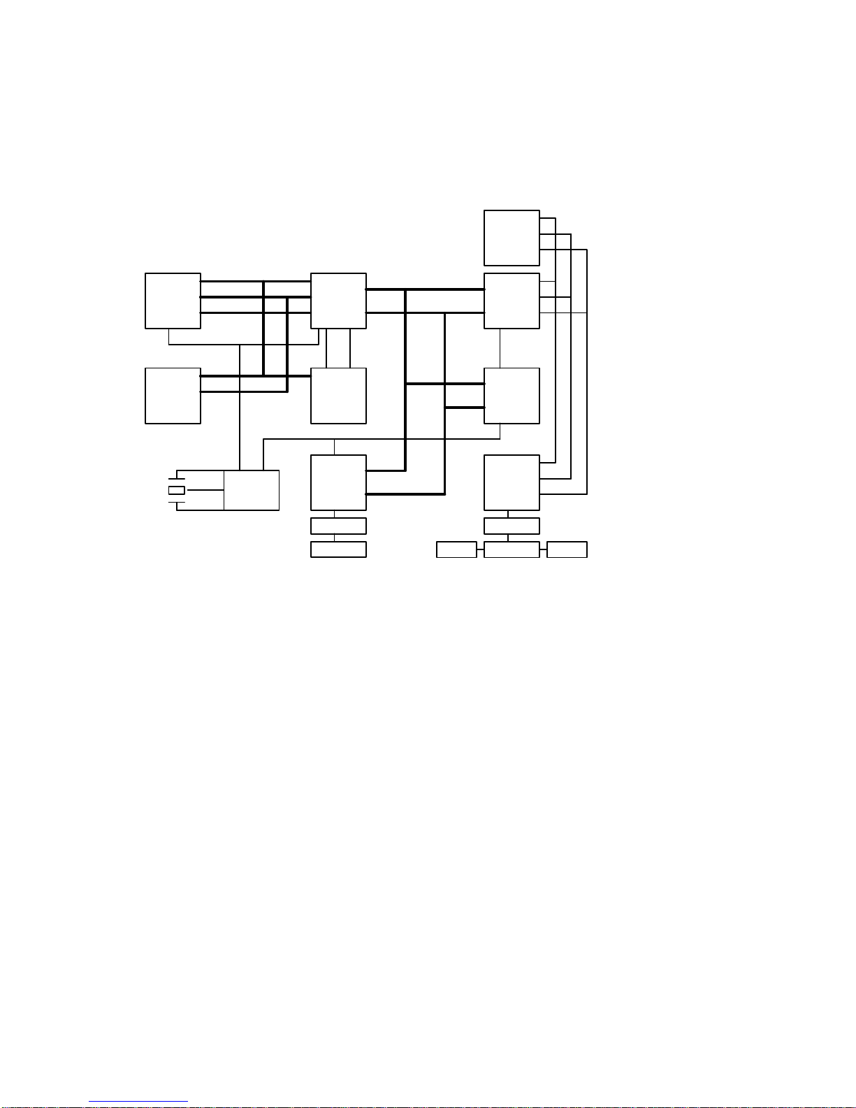
1.4. BLOCK DIAGRAM.................................................................................................7
1.5. INTRODUCE THE PCI - BUS...............................................................................7
1.6. FEATURES............................................................................................................8
2. SPECIFICATION ............................................................................................................9
2.1. HARDWARE .........................................................................................................9
2.2. SOFTWARE..........................................................................................................10
2.3. ENVIRONMENT.................................................................................................... 10
3. HARDWARE INSTALLATION........................................................................................ 11
3.1. UNPACKING............................................................................................................ 11
3.2. MAINBOARD LAYOUT............................................................................................ 12
3.3. QUICK REFERENCE FOR JUMPERS & CONNECTORS.....................................12
3.4. DRAM INSTALLATION............................................................................................ 14
3.5. SRAM INSTALLATION AND JUMPERS SETUP....................................................15
3.6. CPU INSTALLATION AND JUMPERS SETUP.......................................................15
3.7. CMOS RTC & ISA CFG CMOS SRAM...................................................................16
3.8. SPEAKER CONNECTOR INSTALLATION.............................................................16
3.9. POWER LED & KEY LOCK CONNECTOR INSTALLATION .................................16
3.10. TURBO SWITCH CONNECTOR INSTALLATION................................................16
3.11. TURBO LED CONNECTOR INSTALLATION....................................................... 17
3.12. HARDWARE RESET SWITCH CONNECTOR INSTALLATION.......................... 17
3.13. PERIPHERAL DEVICE INSTALLATION............................................................... 17
4. BIOS CONFIGURATION................................................................................................ 18
4.1. ENTERING SETUP...............................................................................................18
4.2. CONTROL KEYS...................................................................................................18
4.3. GETTING HELP ....................................................................................................19
4.3.1. Main Menu.................................................................................................... 19
4.3.2. Status Page Setup Menu / Option Page Setup Menu .................................19
4.4. THE MAIN MENU..................................................................................................19
4.5. STANDARD CMOS SETUP MENU...................................................................... 21

GA-586AL
________________________________________________________________
________________________________________________________________
4
4.6. BIOS FEATURES SETUP..................................................................................... 24
4.7. CHIPSET FEATURES SETUP..............................................................................27
4.8. PCI SLOT CONFIGURATION............................................................................... 29
4.9. LOAD SETUP DEFAULTS ...................................................................................... 31
4.10. PASSWORD SETTING.......................................................................................32
4.11. IDE HDD AUTO DETECTION.............................................................................33
4.12. HDD LOW LEVEL FORMAT...............................................................................33
4.13. SAVE & EXIT SETUP..........................................................................................34
4.14. EXIT WITHOUT SAVING .................................................................................... 35
4.15. KEYBOARD SETTING FUNCTION.....................................................................35
5. AT TECHNICAL INFORMATION ...................................................................................36
5.1. I/O BUS CONNECTOR PIN OUT.........................................................................36
5.1.1. ISA SLOT PIN OUT...................................................................................... 36
5.1.2. PCI - BUS SLOT PIN OUT........................................................................... 37
5.2. I/O & MEMORY MAP ............................................................................................ 38
5.3. TIMER & DMA CHANNELS MAP......................................................................... 38
5.4. INTERRUPT MAP................................................................................................. 39
5.5. RTC & CMOS RAM MAP...................................................................................... 39
APPENDIX A: POST MESSAGE..........................................................................................40
APPENDIX B: POST CODES...............................................................................................45
APPENDIX C: BIOS DEFAULT DRIVE TABLE.................................................................... 48
APPENDIX D: PROBLEM SHEET........................................................................................50

Introduction
________________________________________________________________
________________________________________________________________
5
1. INTRODUCTION
1.1.PREFACE
Welcome to use the GA - 586AL motherboard. The motherboard is a 256 KB /
512 KB / 1 MB CACHE PENTIUMCPU based PC / AT compatible system with
ISA bus and PCI Local Bus, and has been designed to be the fastest PC / AT
system. There are some new features allow you to operate the system with just
the performance you want.
This manual also explains how to install the motherboard for operation, and how
to set up your CMOS CONFIGURATION with BIOS SETUP program.
1.2.KEY FEATURES
qPentiumbased PC / AT compatible mainboard with PCI - ISA Bus.
q3 Master / Slave PCI Bus slots, 4 ISA Bus slots.
qSupports Pentium / P5T running at 60 / 66 MHz.
qSupports true 64 bits CACHE and DRAM access mode.
qSupports 273 Pins (Socket 4) ZIF white socket on board.
qSupports 256 KB / 512 KB / 1 MB second cache memory.
qCPU L1 / L2 Write-Back cache operation.
qSupports 2 - 160 MB DRAM memory on board.
qSupports 2 channels Enhance PCI IDE ports for 4 IDE Device.
qSupports 2xCOM, 1xLPT, 1x1.44MB Floppy port.
qSupports Hardware and Software speed change function.
qLicensed AWARD BIOS, FLASH EEPROM for BIOS update.
qBENCHMARQ / ODIN 3287 RTC on board.
q3/4BABY AT size, 4 layers PCB.

GA-586AL
________________________________________________________________
________________________________________________________________
6
1.3.PERFORMANCE LIST
The following performance data list is the testing results of some popular
benchmark testing programs. These data are just referred by users, and there is
no responsibility for different testing data values gotten by users.( The different
Hardware & Software configuration will result in different benchmark testing
results.)
lCPU Pentium60 / 66 MHz
lDRAM 16 MB - 70 ns
lCACHE SIZE 256 KB
lDISPLAY ATi Mach64 PCI VGA
lSTORAGE on board IDE + Conner 540MB H.D.
lO.S. MS DOS V6.2
×MAINBOARDØ
Testing Program Item Unit Pentium 66 Pentium 60
LandMark V1.14 CPU MHz 200+ 200+
LandMark V2.0 CPU MHz 385.88 347.29
FPU MHz 1135.31 1021.707
SI V7.0 CPU 211.7 190.6
Byte V2.1 CPU AT Class 25.13 16.43
386 Class 9.22 6.23
FPU AT Class 135.17 121.65
386 Class 18.91 17.02
BenchMark V8.0 Processor Score 77.43 69.61
PM V1.7 MIPS Mips 46.4 41.9
DhryStone K-Dstone/s 59.5 53.2
WhetStone K-Wstone/s 13148.9 11896.6
×IDEØ
Program Ver. Item Unit Pentium 66 Pentium 60
Core 2.92 Data Transfer Rate KB/s 10296.1 9307.1
Average Seek Time ms 10.5 10.5
Track-Track Seek ms 2.9 2.9
Performance Index 66.517 60.661
Winbench 4.0 Disk Winmark KB/s 2500 2350
Benchmark 8.0 Disk Score 1546 1500
PM 1.7 Data Transfer Rate KB/s 32233.8 32233.8
Mean Seek ms/seek 10.7 10.9
Track-Track Seek ms/seek 2.8 2.9
Aggregate PUM's 4883.5 4881.9
Byte 2.1 Disk AT Class 37.35 35.25
386 Class 21.73 20.51
SI Data Transfer Rate KB/s 1958.7 1957.7
Average Seek ms 2.71 2.68
Track-Track Seek ms 10.29 10.23
HDD Index 15.5 15.5
Winstone94 1.0 Winstone 106.5 96.7

Introduction
________________________________________________________________
________________________________________________________________
7
1.4. BLOCK DIAGRAM
×Figure 1.1Ø
CACHE
CPU
ICW
42C25
Data
Address
Control
60/66 MHz
30/33 MHz
14.318 MHz CLOCK Generator
MA RAS
CAS
WE
M1451
DRAM
PCI
IDE
IDE1
IDE2
PCI BUS
ISA
SLOT1-4
M1449
UMC
I/O
Floppy
LPTCOM1 COM2
ISA BUS
PCI
SLOT1-3
AD
Control
1.5.INTRODUCE THE PCI - BUS
Connecting devices to a CPU local bus can dramatically increase the speed of
I/O-bound peripherals with only a slight increase in cost over traditional systems.
This price / performance point has created a vast market potential for local bus
products. The main barrier to this market has been the lack of an accepted
standard for local bus peripherals. Many mainboard and chipset manufactures
developed their own local bus implementations, but they are incompatible with
each other. The VL (Video Electronics Standards Association) local bus and PCI
(Peripheral Component Interconnect) bus specification was created to end this
confusion.
The PCI - bus standard, under development since Jun. 1992, which is designed
to bring workstation-level performance to standard PC platform. The PCI - bus
removes many of the bottlenecks that have hampered PC for several years. On
the PCI - bus, peripherals operate at the native speed of the computer system,

GA-586AL
________________________________________________________________
________________________________________________________________
8
thus enabling data transfer between peripherals and the system at maximum
speed. This performance is critical for bandwidth-constrained devices such as
video, multimedia, mass storage, and networking adapters.
PCI - bus standard provides end-users with a low-cost, extendible and portable
local bus design, which will allow system and peripherals from different
manufactures to work together.
1.6.FEATURES
q32 bits bus transfer mode.
qBus Master or Slave access.
qMemory burst transfer to 132 MB/sec.
q33 MHz operation speed.
q10 device loading ability.
qCPU independent.

Specification
________________________________________________________________
________________________________________________________________
9
2. SPECIFICATION
2.1.HARDWARE
lCPU −Pentium60 / 66 MHz, P5T.
−273 pins (socket 4) ZIF white socket on board.
lCOPROCESSOR −Included in Pentium.
lSPEED −60 / 66 MHz system and 30 / 33 PCI-Bus speed.
−7.5 / 8 MHz AT bus speed.
−Hardware and Software speed switchable
function (half speed).
lDRAM MEMORY −3 banks 72 pins SIMM module socket on board
(2 for Double banks, 1 for Single bank).
−
Use 1 / 2 / 4 / 8 / 16 / 32 MB 70 ns SIMM module
DRAM.
−2 ~ 160 MB DRAM size.
−Support Fast Page DRAM access mode.
lCACHE MEMORY −16 KB cache memory included in Pentium.
−256 KB / 512 KB / 1 MB second cache memory
on board.
−
Support Write Back cache function for both CPU
& on board cache.
lSHADOW RAM −Main BIOS shadow function.
−Video BIOS shadow function programmable.
−Shadow RAM cacheable function.
lI/O BUS SLOTS −3 Master / Slave PCI-Bus.
−4 16 bits ISA Bus.
lIDE PORTS −2 Enhanced IDE channels on board.
(Using IRQ14,15)
−Support Mode 3, 4 IDE & ATAPI CD - ROM.
−Driver Support DOS, WINDOWS, OS/2, NT,
UNIX, Netware.
lI/O PORTS −Supports 2 16450 COM ports. (Using IRQ4,3)
−Supports 1 LPT port.(Using IRQ7)
−Supports 1 1.44MB Floppy port.
(Using DMA2 & IRQ6)
lBIOS −128KB FLASH EEPROM.
lDIMENSION −3/4Baby AT size / 4 layers.

GA-586AL
________________________________________________________________
________________________________________________________________
10
2.2.SOFTWARE
lBIOS −Licensed AWARD BIOS.
−AT CMOS Setup, BIOS / Chipset Setup and
Hard Disk Utility included.
lO.S. & IDE DRIVER
−
Operation with MS-DOS, WINDOWS NT, OS/2,
NOVELL and SCO UNIX.
2.3.ENVIRONMENT
lAmbient Temp. −0°C to +50°C (Operating).
lRelative Hum. −0 to +85% (Operating).
lAltitude −0 to 10,000 feet (Operating).
lVibration −0 to 1,000 Hz.
lElectricity −4.9 V to 5.2 V.
−5 A to 7 A current.

Hardware Installation
________________________________________________________________
________________________________________________________________
11
3. HARDWARE INSTALLATION
3.1. UNPACKING
The mainboard package should contain the following:
lThe GA - 586AL mainboard.
lDiskette for Enhanced IDE Device Driver ( 1 x 1.44MB Diskette).
lUSER'S MANUAL.
lCable set for I/O Device.
The mainboard contains sensitive electric components which can be easily
damaged by static electricity, so the mainboard should be left in its original
packing until it is installed.
Unpacking and installation should be done on a grounded anti-static mat. The
operator should be wearing an anti static wristband, grounded at the same point
as the anti-static mat.
Inspect the mainboard carton for obvious damage. Shipping and handling may
cause damage to your board. Be sure there are no shipping and handling
damages on the board before proceeding.
After opening the mainboard carton, extract the system board and place it only
on a grounded anti-static surface component side up. Again inspect the board
for damage. Press down on all of the socket IC's to make sure that they are
properly seated. Do this only on with the board placed on a firm flat surface.
M
DO NOT APPLY POWER TO THE BOARD IF IT HAS BEEN DAMAGED.
You are now ready to install your maniboard. The mounting hole pattern on the
mainboard matches the IBM-AT system board. It is assumed that the chassis is
designed for a standard IBM XT/AT mainboard mounting.
Place the chassis on the anti-static mat and remove the cover. Take the plastic
clips, Nylon stand-off and screws for mounting the system board, and keep them

GA-586AL
________________________________________________________________
________________________________________________________________
12
separate.
3.2. MAINBOARD LAYOUT
×Figure 3.1Ø
BIOS
RTC
DS12887
27C010
ISA SLOT 1
ISA SLOT 2
ISA SLOT 3
ISA SLOT 4
PCI SLOT #3
PCI SLOT #2
PCI SLOT #1 & I/O
BIOS
KBD
CPU
66 MHz
60 MHz
JP21
BANK 0
BANK 1
72 PIN SIMM MODULE
72 PIN SIMM MODULE
+
SOCKET 4
Pentium
JP3
+12V Second
Cache
P5T
P1
P3
BANK 2
72 PIN SIMM MODULE
U25
1
1
1
1
1
1
1 72
72
72
72
72
72
72
3
1
1
JP2 JP1
JP17
JP20
JP19
JP18
JP16
11
1
SIMM1
SIMM6
1
1 1
LPT PORT CN6
CN4
FLOPPY PORTIDE1
IDE2 CN5
CN3
JP5
HD-LED
JP14
JP13
CN1
CN2
GA - 586AL
REV.2
COM 1/3
COM 2/4
+
+
3.3. QUICK REFERENCE FOR JUMPERS & CONNECTORS
tP1: Keyboard Connector
Pin No. Function
1Key Clock.
2Key Data.
3NC.
4VCC (+5V).
5GND.
tP2: Power Connector
Pin No. Function
1Power Good signal
2,10,11,12 VCC (+5V)
3+12V
4-12V
5,6,7,8 GND
9-5V

Hardware Installation
________________________________________________________________
________________________________________________________________
13
tJP16: Reset Switch
Open For normal operation.
Close For hardware reset system.
tJP17: Power LED and Key-Lock Connector
Pin No. Function
1LED anode (+).
2NC.
3LED cathode (-).
4Key lock.
5GND.
tJP18: Turbo Switch
Pin No. Function
Close For low speed (Non-cache).
Open For high speed.
tJP19: Turbo LED Connector
Pin No. Function
1LED cathode (+).
2LED anode (-).
tJP20: Speaker Connector
Pin No. Function
1VCC.
2NC.
3GND.
4Data.
tJP1 JP2 Second Cache Size Selection
Pin No. Function
1-2 1-2 Close for 256 KB cache size ( using 32K x 8 SRAM ).
1-2 2-3 Close for 512 KB cache size ( using 64K x 8 SRAM ).
2-3 2-3 Close for 1 MB cache size ( using 128K x 8
SRAM ).
tJP21: System Speed Selection
Pin No. Function
1-2 Close for 60 MHz system speed.
2-3 Close for 66 MHz system speed.

GA-586AL
________________________________________________________________
________________________________________________________________
14
tJP3: CPU Cooling Fan Power Connector
Pin No. Function
1+12V
2GND
tCN1-6 I/O Ports Connector
CN1 For COM 1/3 (Serial port1 )
CN2 For COM 2/4 (Serial port2 )
CN4 For Floppy port
CN6 For LPT port
CN3 For Primary IDE port
CN5 For Secondary IDE port
3.4. DRAM INSTALLATION
The mainboard can be installed with 1 / 2 / 4 / 8 / 16 / 32 MB 72 pins SIMM
module DRAM, and the DRAM speed must be 70 ns. The DRAM memory system
on mainboard consists of bank 0, 1 & bank 2. The DRAM of any bank can be
installed first. Each bank consist of 2 PCs, 72 pins SIMM module DRAM.
Because the 72 pins SIMM module is 32 bits width, using 2 PCs which can
match a 64 bits system. The total memory size is 2 - 160 MB, and various
configuration of DRAM types in the following TABLE are available:
Bank 0 Bank 1 Bank 2 Single: Single bank SIMM Module
Single None None Ex. 1MB, 4MB, 16MB
Single Single
Single Single Single Double: Double banks SImm Module
Double None None Ex. 2MB, 8MB, 32MB
Double Single None
Double Single Single
Double Single Double
The DRAM installation position refer to Figure 3.1, and notice the Pin 1 of SIMM
module must match with the Pin 1 of SIMM socket when the DRAM SIMM
module is installed.
Insert the DRAM SIMM module into the SIMM socket at 45 degree angle. If there
is a wrong direction of Pin 1, the DRAM SIMM module couldn't be inserted
into socket completely. After completely insert SIMM module into socket, then
press the SIMM module in vertical direction until the left and right metal holders
can keep the SIMM module standing up con-firmly.

Hardware Installation
________________________________________________________________
________________________________________________________________
15
3.5. SRAM INSTALLATION AND JUMPERS SETUP
The cache memory system consists of Data SRAM & TAG SRAM (U12), the
Data SRAM type is 32Kx8-15/20 ns, 64Kx8-15/20 ns or 128Kx8-15/20 ns.
The mainboard can be installed with 256 KB, 512 KB or 1 MB cache memory
when using 32Kx8, 64Kx8, 128Kx8 type DATA SRAM separately. Please refer to
the following table to install cache memory system :
SIZE Data SRAM JP2 JP1 TAG SRAM (U12)
256 KB 32 KB x 8 1 - 2 1 - 2 8 KB x 8 - 32 K x 8
512 KB 64 KB x 8 2 - 3 1 - 2 16 KB x 8,32 K x 8
1
MB 128 KB x 8 2 - 3 2 - 3 32 KB x 8
Because there are not standard IC's coding number of SRAM, refer to the
following table to identify the SRAM component:
16 K x 8 32 K x 8 64 K x 8 128 K x 8
AE88128AK-15 W24257AK-15/20 W24512AK-15/20 W241024AK-15/20
UM61256-15/20 AS7C512-15/20 AS7C1024-15/20
AS7C256-15/20 UM61512AK-15/20 UM611024AK-15/20
CY7C199-20
MCM6206-20
KM68257BP-20
TC555328P-20
3.6. CPU INSTALLATION AND JUMPERS SETUP
The system's speed depends on the frequency of CLOCK GENERATOR. The
user can change the JUMPER (JP21) selection to set up the system speed to 60
MHz or 66 MHz for 60 or 66 MHz PENTIUMCPU.
The mainboard can use PENTIUMor P5T CPU, and the CPU speed must
match with the frequency of CLOCK GEN. It will cause system hanging up if the
CLOCK GEN.'S frequency is higher than CPU's.
JP21 CPU Type CLK. GEN. Speed CPU Speed
2 - 3 PENTIUM- 66 66.667 MHz 66.667 MHz
1 - 2 PENTIUM- 60 60 MHz 60 MHz

GA-586AL
________________________________________________________________
________________________________________________________________
16
M
The CPU is a sensitive electric component and it can be easily damaged
by static electricity, so users must keep it away from metal surface
when the CPU is installed onto mainboard.
M
When the user installs the CPU on socket, please notice the PIN 1 of
CPU is in the same corner as the PIN 1 of socket!
M
Before the CPU is installed, the mainboard must be placed on a flat
plane in order to avoid being broken by the pressure of CPU installation.
3.7. CMOS RTC & ISA CFG CMOS SRAM
There're RTC & CMOS SRAM on board, they have a power supply from internal
battery to keep the DATA inviolate & effective. The RTC is a REAL-TIME
CLOCK device which provides the DATE & TIME to system. The CMOS SRAM
is used for keeping the information of ISA device system configuration, so the
system can automatically boot OS. every time.
Due to the life-time of RTC internal battery is 10 years, the user can change a
new RTC to replace old one after it can not work. The new one's brand and type
must be same with old one.
3.8. SPEAKER CONNECTOR INSTALLATION
There is always a speaker in AT system for sound purpose. The 4 - Pins
connector JP20 is used to connect speaker. The speaker can work well in both
direction of connector when it is installed to the connector JP20 on mainboard.
3.9. POWER LED & KEY LOCK CONNECTOR INSTALLATION
There are a system power LED lamp and a key on the panel of case. The power
LED will light on when system is powered-on, and the key can lock the keyboard
input or unlock it, both of them are connected to a 5 PIN connector. The
connector should be installed to JP17 of mainboard in correct direction.
3.10. TURBO SWITCH CONNECTOR INSTALLATION
The TURBO switch on the panel is used for controlling the system speed. Some

Hardware Installation
________________________________________________________________
________________________________________________________________
17
program developed on XT should be executed with a low speed system, so a
high speed system needs the speed switching function to change its running
speed.
The mainboard uses helf speed method to implement TURBO switching function.
The JP18 on mainboard should be connected to the TURBO switch on panel,
and user can push in or pop out the TURBO switch to enable or disable the
turbo function of system.
M
If not necessary, please don't use De-turbo mode. (always keep system
in Turbo mode)
3.11. TURBO LED CONNECTOR INSTALLATION
The TURBO LED on panel can indicate the current speed status of system. The
TURBO LED connector should be installed to JP19 in correct direction.
3.12. HARDWARE RESET SWITCH CONNECTOR INSTALLATION
The RESET switch on panel provides users with HARDWARE RESET function
which is almost the same as power-on/off. The system will do a cold start after
the RESET switch is pushed and released by user. The RESET switch is a 2 PIN
connector and should be installed to JP16 on mainboard.
3.13. PERIPHERAL DEVICE INSTALLATION
After the device installation and jumpers setup, the mainboard can be mounted
into the case and fixed by screw. To complete the mainboard installation, the
peripheral device could be installed now. The basic system needs a display
interface card and a disk device.
If the PCI - Bus device is to be installed in the system, any one of three PCI -
Bus slots can be used no matter Slave or Master PCI - Bus device being
installed.
After installing the peripheral device, the user should check everything again,
and prepare to power-on the system.

GA-586AL
________________________________________________________________
________________________________________________________________
18
4. BIOS CONFIGURATION
Award's BIOS ROM has a built-in Setup program that allows users to modify the
basic system configuration. This type of information is stored in battery-backed
CMOS SRAM so that it retains the Setup information when the power is turned
off.
4.1.ENTERING SETUP
Power ON the computer and press <Del> immediately will allow you to enter
Setup. The other way to enter Setup is to power on the computer, when the
below message appears briefly at the bottom of the screen during the POST
(Power On Self Test), press <Del> key or simultaneously press <Ctrl>, <Alt>,
and <Esc> keys.
•TO ENTER SETUP BEFORE BOOT PRESS CTRL-ALT-ESC OR DEL KEY
If the message disappears before you respond and you still wish to enter Setup,
restart the system to try again by turning it OFF then ON or pressing the
"RESET" bottom on the system case. You may also restart by simultaneously
press <Ctrl>,<Alt>, and <Del> keys. If you do not press the keys at the correct
time and the system does not boot, an error message will be displayed and you
will again be asked to,
•PRESS F1 TO CONTINUE, CTRL-ALT-ESC OR DEL TO ENTER SETUP
4.2.CONTROL KEYS
Up arrow Move to previous item
Down arrow Move to next item
Left arrow Move to the item in the left hand
Right arrow Move to the item in the right hand
Esc key Main Menu - Quit and not save changes into CMOS
Status Page Setup Menu and Option Page Setup Menu - Exit
current page and return to Main Menu
PgUp key Increase the numeric value or make changes
PgDn key Decrease the numeric value or make changes
F1 key General help, only for Status Page Setup Menu and Option Page
Setup Menu
F2 key Change color from total 16 colors
F3 key Calendar, only for Status Page Setup Menu
F4 key Reserved
F5 key Restore the previous CMOS value from CMOS, only for Option
Page Setup Menu
F6 key Load the default CMOS value from BIOS default table, only for
Option Page Setup Menu

BIOS Configuration
________________________________________________________________
________________________________________________________________
19
F7 key Load the default
F8 key Reserved
F9 key Reserved
F10 key Save all the CMOS changes, only for Main Menu
4.3.GETTING HELP
4.3.1.Main Menu
The on-line description of the highlighted setup function is displayed at the
bottom of the screen.
4.3.2.Status Page Setup Menu / Option Page Setup Menu
Press F1 to pop up a small help window that describes the appropriate keys to
use and the possible selections for the highlighted item. To exit the Help
Window press <Esc>.
4.4.THE MAIN MENU
Once you enter Award BIOS CMOS Setup Utility, the Main Menu (Figure 4.1) will
appear on the screen. The Main Menu allows you to select from seven setup
functions and two exit choices. Use arrow keys to select among the items and
press <Enter> to accept or enter the sub-menu.
Figure 4.1: Main Menu
ROM PCI / ISA BIOS
CMOS SETUP UTILITY
AWARD SOFTWARE, INC.
STANDARD CMOS SETUP
BIOS FEATURES SETUP
CHIPSET FEATURES SETUP
PCI CONFIGURATION SETUP
LOAD SETUP DEFAULTS
PASSWORD SETTING
IDE HDD AUTO DETECTION
SAVE & EXIT SETUP
EXIT WITHOUT SAVING
ESC
F10 : Quit
: Save & Exit Setup (Shift)F2 : Select Item
: Chang Color
Time, Date, Hard Disk Type, ...
HDD LOW LEVEL FORMAT

GA-586AL
________________________________________________________________
________________________________________________________________
20
•Standard CMOS setup
This setup page includes all the items in a standard compatible BIOS.
•BIOS features setup
This setup page includes all the items of Award special enhanced features.
•Chipset features setup
This setup page includes all the items of chipset special features.
•PCI configuration setup
This setup page includes all the configurations of PCI slots parameters
•Load setup defaults
BIOS defaults indicates the most appropriate value of the system parameter which the
system would be in maximum performance.
•Password setting
Change, set, or disable password. It allows you to limit access to the system and Setup, or
just to Setup.
•IDE HDD auto detection
Automatically configure hard disk parameter.
•HDD LOW level format
Low level format IDE Hard disk.
•Save & exit setup
Save CMOS value changes to CMOS and exit setup.
•Exit without save
Abandon all CMOS value changes and exit setup.
This manual suits for next models
1
Table of contents
Other Pentium Motherboard manuals

Pentium
Pentium GA - 586ATV User manual

Pentium
Pentium GA-8IDML Series User manual

Pentium
Pentium P51437P4/FMB User manual

Pentium
Pentium 6EA User manual

Pentium
Pentium 5VD2 Use and care manual

Pentium
Pentium P51430TX-250 User manual

Pentium
Pentium 82430 VX/P54C Use and care manual

Pentium
Pentium Explorer IV User manual

Pentium
Pentium P55-IT User manual

Pentium
Pentium GA - 586IP User manual