Philco 57 User manual


1. PRAFACE
1.1 PRAFACE.....................................................................................................................1
1.2 FRANT PENEL& REAR PENEL.....................................................................................2
1.3 REMOTE CONTROL............................................................................. .......................3
2. BLOCK DIAGRAM
2.1 BLOCK DIAGRAM........................................................................................................4.
2.2 SCHEMATIC DIAGRAM.................................................................................................5
3. EXPLODED VIEW......................................................................6
4. PARTS SPECIFICATIONS
4.1 2A265.....................................................................................................................7-10
4.2 CS9800.................................................................................................................11-18
4.3 DRAM 2M*32(EM638165).......................................................................................19-22
4.4 CS4955.................................................................................................................23-25
4.5 CS4360.................................................................................................................26-30
4.6 CS92288...............................................................................................................31-45
4.7 DRAM 1M*16(VT3617161)......................................................................................46-49
4.8 SAA7114H.............................................................................................................50-57
4.9 CS533...................................................................................................................58-59
4.10 PCF8563.............................................................................................................60-62
4.11 TUNER................................................................................................................... .63
4.12 VFD DRIVER PT6312.................................................................... ......................64-65
4.13 SERVO............................................................................................. .......................66
4.14 HDD INFORMATION.............................................................................................67-68
5. SCHEMATIC DIAGRAM
5.1 POWER SCHEMATIC..................................................................... .......................69-70
5.2 MAIN SCHEMATIC......................................................................... .......................71-79
5.3 AV INPUT /OUTPUT SCHEMATIC.................................................... ...................... 80-87
5.4 VFD DRIVER........................................................................................................ 88-89
6. PARTS LIST
6.1 MAIN BOARD........................................................................................................90-92
6.2 VFD DRIVER BOARD.......................................................................... .......................93
6.3 POWER BOARD....................................................................................................94-95
6.4 AV BOARD.................................................................................................................96
INDEX
INDEX
INDEX

PREFACE
INTRODUCTION
This unit has DVD play function and hard disc videotape function. Under DVD PLAY mode, you can
play all kinds of disc; under TV mode, you can receive TV programs, under AV mode, you can receive
programs from exterior signal resources. In these mode above, you can press the key of REC to
videotape program; you can also watch DVD disc or recorded program while recording the TV program.
By using the TIME-SHIFT mode of the product, you can press TIMESHIFT key when you have to leave
the program, you can enjoy it later when you return, because the unit has recorded it into its hard disc;
you can then watch it and control it by pressing REWIND/FORWARD keys. Add simply press a key to
save the program. A time-set function let you not miss any wonderful TV programs. What you have to
do is to pre-set the function. The unit has a great capability of videotaping, you can use several kinds
of pre-set functions for videotaping. You can also respectively set the videotape time,image quality
level (the best image quality level is like a DVD image).
FEATURES
Built-in 40G Hard Disk Drive is capable for Extra Long-time Recording, High Speed Accessing and
Iterative Rewriting.
Built-in 5.1CH Dolby Digital Surround Decoder is compatible with Dolby PRO LOGIC
Suitable for playing DVD/SVCD/VCD/CD-DA/MP3
Utilizing MPEG-II Digital Real-Time Encoding and Decoding Technology. Supporting for 4 level
picture quality recording modes
The outstanding up to 2-Hour Time shifting function enables enjoying the control of the TV Programs
freely by Pause, Fast Forward/Rewind and Slow Playback of the TV Programs.
Intelligent Preset Timing Recording Function enables the recording tasks in different periods of time.
The timing recording tasks can be activated even when the machine is at standby mode. You will
never miss any desired TV programs at any time.
With the TV Tuner/AV/S-Video input terminals, it is convenient to record any program sources such
as the signal from CATV/Disc Player/Video Camera.
Composite, S-Video, Component Video (YCbCr) output and 5.1CH audio output, Optical/Coaxial
Digital Audio Output.
Extremely low consumption of power during standby period ( 1W) featuring energy efficiency and
safety.
Built-in TV Tuner enables automatic TV Channel searching and saving
Powerful program managing function providing program free playback, erasing, locking or renaming.
Simultaneously recording and playing of the real-time TV Programs are available.
Built-in real-time calendar and clock can normally work even when the power is plugged off.
Recording and output system is optional between PAL and NTSC system
1

GENERAL INFORMATION
FRONT PANEL
REAR PANEL
TV TUNER input terminal
1
COMPOSITE VIDEO input terminal
2
AUDIO input terminal
3
COMPOSITE VIDEO output terminal
6
45.1CH AUDIO output terminals
5MIXED AUDIO output terminals
COMPONENT VIDEO output terminals
7
S-VIDEO input terminal
8
S-VIDEO output terminal
9
10 COAXIAL output terminal for digital audio
11 OPTICAL output terminal for digital audio
1 2 3568 9 10
Press to switch the player on/off
STANDBY/ON
1
2STANDBY INDICATOR LIGHT
Turn on in red when standby, otherwise
turn off
Displays information on the
status of the DVR
4
Recording start
REC button
5
6DISC TRAY
When loading a disc, place disc in the
disc tray with the label side facing up
7
Press to stop playback or recording
STOP button
9
7OPEN/CLOSE button
Open/close button for the disc tray
3DVD FUNCTION button
Switch to the DVD mode
Switch to TV/AV modes
TV/AV FUNCTION button
4
8PLAY/PAUSE button
Playback/pause playing
1 32 4 5
8 9
6 7
10
12
VFD
11
11
INFRARED SENSOR
12
10 CH+/- and PREV/NEXT button
Skip to back channelnext /
Skip to back track / chapter and next
track / chapter
11
2

GENERAL INFORMATION
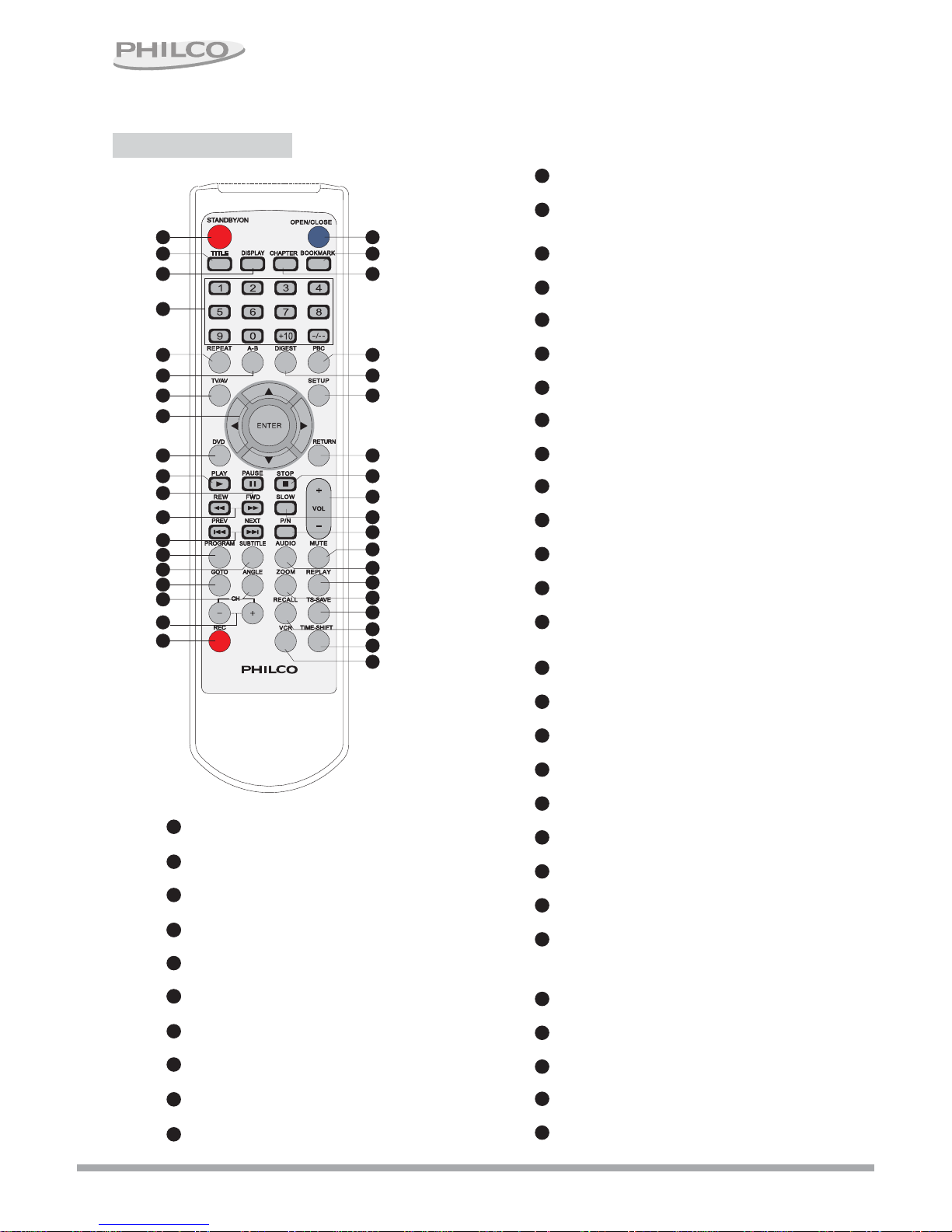
REMOTE CONTROL
1
2
3
4
5
6
7
8
9
10
11
12
13
14
15
16
17
18
19
20
21
22
23
24
25
26
27
28
29
30
31
32
33
34
36
37
35
Repeat a specific segment (A-B)
6
A-B button
Change camera angles
ANGLE button
17
5
REPEAT button
Repeat playback
Skip to back track/chapter and next track/chapter
13 PREV/NEXT buttons
Switch between standby and working status
STANDBY/ON button
1
Switch to TV/AV modes
7TV/AV button
9DVD buttons
Switch to DVD mode
Press to bookmark memory playback
21 BOOKMARK button
Press to simultaneously view 9 pictures on screen
24 DIGEST button
NTSC/PAL conversion
P/N button
30
Zoom in the displayed frame
ZOOM button
27
34
Backward 5 seconds
33 REPLAY button
Skip to previous channel
36 RECALL button
2
TITLE button
Show the title of disk. When activated,
allows the user to select the desired title for playback
NUMBER buttons
4
Number selection
15 SUBTITLE buttons
Press to select the subtitle languages for your preference
CURSOR buttons
8
Arrow selection. (OSD navigation buttons)
PLAY button
10
Playback
STOP button
27
Press to stop playback or recording.
12 REW/FWD button
Rewind / Fast Forward playback
14 PROGRAM button
In AV/TV mode, press PROG button to activate
the HDD content and then playback
3
DISPLAY button
Open/Close the screen display
16
GOTO button
Search specific time or track/ title/ chapter to play
18 CH+/- button
Skip to back channelnext /
19 REC button
Recording start button.
20 OPEN/CLOSE button
Open/Close the disk tray
25 SETUP button
Activate the setup menu
26 RETURN button
Return to last menu
11 PAUSE button
Pause playing or used in Still
29
SLOW button
To Playback at slower speed(1/2; 1/4; 1/8)
28 VOL+/- button
Change the volume of analog audio
MUTE button
31
Select mute on/off the analog audio
37 TIME-SHIFT button
Play buffer to TV
35 TS-SAVE button
Save the buffer of time-shift
22 CHAPTER button
Search specific chapter to play
38
38 VCR button
Enter/exit VCR mode
AUDIO button
27
32
Select different audio channels 23 PBC button
While playing a disc of VCD 2.0, it's used for switching ON/OFF on
play menu.
While playing the disc of DVD, its' used for returning a master menu.
HD-DVD57
3

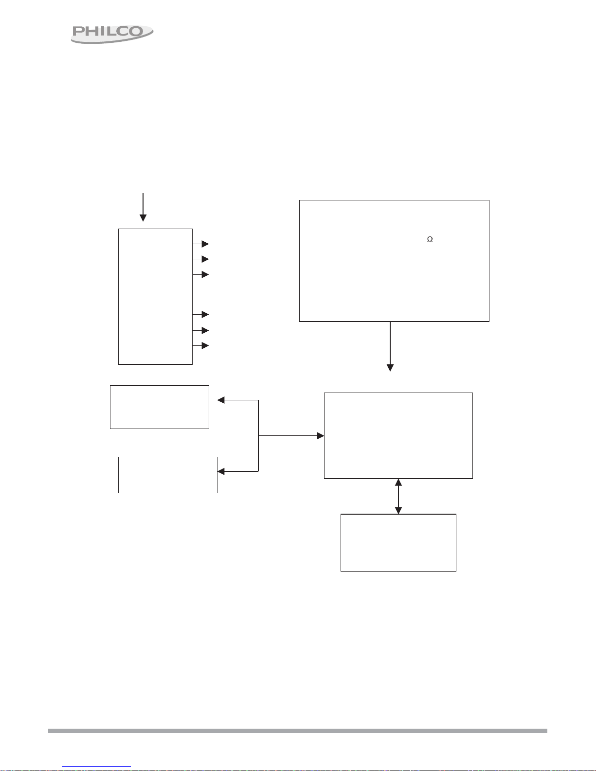
POWER
BOARD
VIDEO OUT VIDIO IN PUT
AUDIO OUT AUDIO IN PUT
TUNER75 IN PUT
S-VIDEO OUT
CB.CR.YOUT
COAXIAL OUT
OPTICAL OUT
AV BOARD
MAIN BOARD
MPEG VIDEO DECODER&
MPEG-2
AUDIO/ VIDEO CODER
DVD LOADER
DRIVE
40GB HDD
40GB HDD DRIVE
PT16312
KEY SCANNING &
VFD DISPLAY
~110~240V
+12V
+5V
-12V
+3.3V
+2.5V
+1.8V
4
BLOCK DIAGRAM

SS9800
MPEG
DECODER
CS92288
MPEG-2
A/V CODEC
CS4955
VIDEO
—— D/A
ENCODER
CS4360
AUDIO
DACS
CS5331
AUDIO
ADC
AUDIO
L.R CH
SAA7114
VIDEO
DECOD
ER
S-VIDEO
TO-TUNER
CPLD
ATAPI
TO DVD LOADER DRIVE
HDD ATAPI I/O CHAN
DRAM
1M*16 4PCS
DRAM
2M*32
FLASH
16M TO VFD BOARD
CN104
P-CTL
5VSTB
1.8V
2.5V
VCC
3.3V
TO S-VIDEO
TO TUNER
AUDIO L3CH
COMPOSITE VIDEO
AUDIO R(3CH)
Host interface
To front panel
To front panel
S-VIDEO
5
SCHEMATIC DIAGRAM

1
2
3
4
5
6
7
8
9
10
11
12
13
14
15
16
17
19
18
20
21
24
23
22
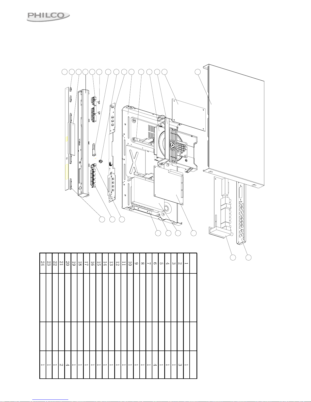
NO. ITEM NAME MATERIAL QUANTITY
Mirror bar pc
Left decorative bar ABS
Tray door ABS
Front panel ABS
Left four-key button ABS
Small light conductor PMMA
Big light conductor PMMA
LED stander PS
VFD driver board
Chasis SECC
Loader mechanism PS
DVD loader
Iron stand SECC
Power board
Top cover SECC
Rear panel SECC
AV board
Main board
Hard disc
Copper column
Rubber pad RUBBER
Open/close button ABS
Right four-key button ABS
Right decorative bar ABS
EXPLODED VIEW
6

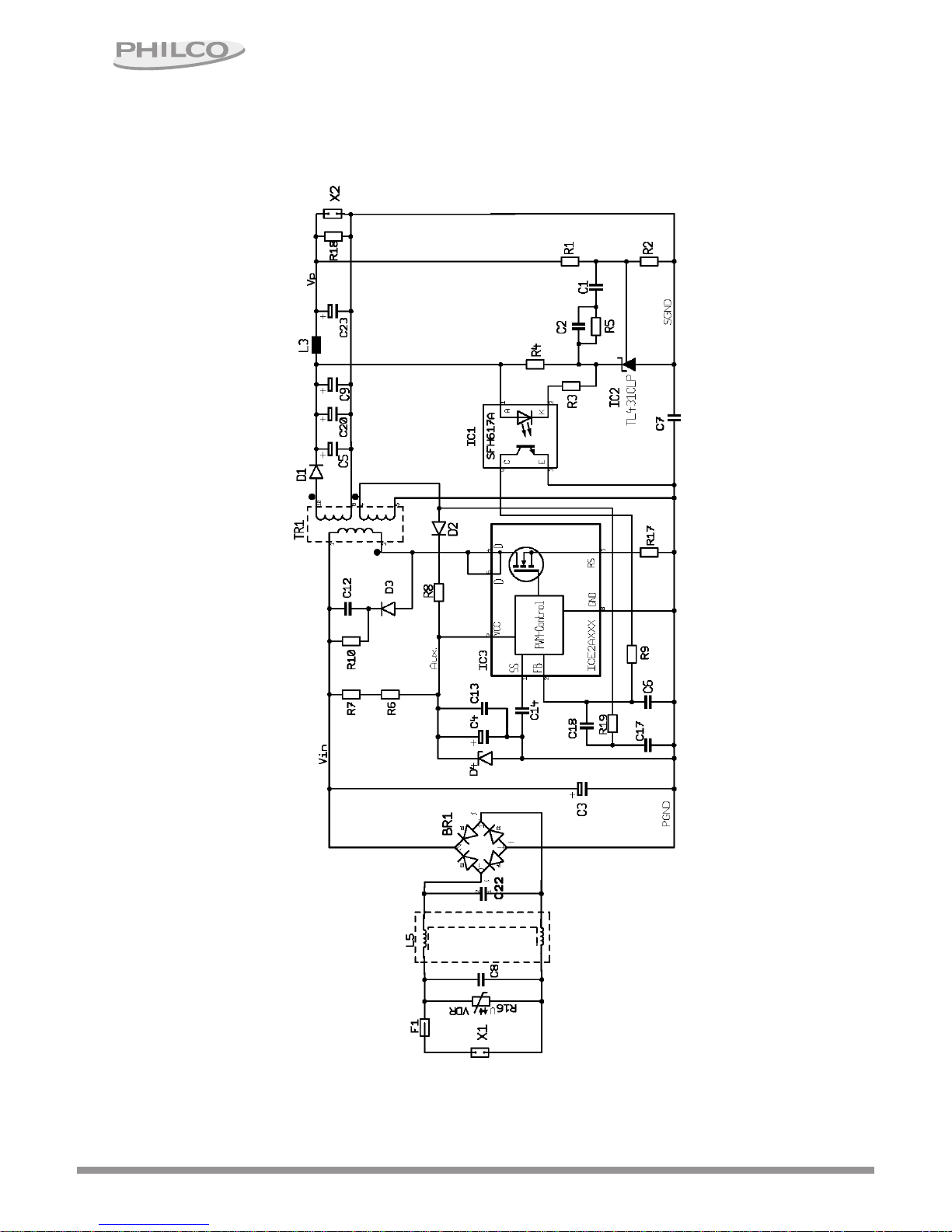
Circuit Diagram: ICE2AXXX for OFF ¨C Line Switch Mode Power Supplies
7

ICE2AXXX for OFF – Line Switch Mode Power Supplies
Protection Functions
The block diagram displayed in Fig. 4 shows the interal functions of the protection unit. The
comparators C1, C2, C3 and C4 compare the soft-start and feedback-pin voltages. Logic gates
connected to the comparator outputs ensure the combination of the signals and enables the setting of
the “Error-Latch”.
8

ICE2AXXX for OFF – Line Switch Mode Power Supplies
Overload and Open-Loop Protection
•Feedback voltage (VFB) exceeds 4.8V and soft start
voltage (VSS) is above 5.3V (soft start is completed) (t1)
•After a 5µs delay the CoolMOS is switched off (t2)
•Voltage at Vcc – Pin (VCC) decreases to 8.5V (t2)
•Control logic is switched off (t3)
•Start-up resistor charges Vcc capacitor (t3)
•Operation starts again with soft start after Vcc voltage
has exceeded 13.5V (t4)
Fig. 6
Fig. 7
t1 t2 t3 t4
V
CC
VFB
VSS
t1, t2
t1
,
t2
t3 t4
V
CC
VFB
VSS
9

ICE2AXXX for OFF – Line Switch Mode Power Supplies
References
[1] Keith Billings,
Switch Mode Power Supply Handbook
[2] Ralph E. Tarter,
Solid-State Power Conversion Handbook
[3] R. D. Middlebrook and Slobodan Cuk,
Advances in Switched-Mode Power Conversion
[4] Herfurth Michael,
Ansteuerschaltungen für getaktete Stromversorgungen mit Erstellung eines linearisierten
Signalflußplans zur Dimensionierung der Regelung
[5] Herfurth Michael,
Topologie, Übertragungsverhalten und Dimensionierung häufig eingesetzter
Regelverstärker
[6] Infineon Technologies, Datasheet,
CoolSET-II
Off – Line SMPS Current Mode Controller with 650V/800V CoolMOSä
ää
äon Board,
[7] Robert W. Erickson,
Fundamentals of Power Electronics
10

Preliminary Product Information
This document contains information for a new product.
Cirrus Logic reserves the right to modify this product without notice.
CS98000
Internet DVD (iDVD) Chip Solution
Features
l
Powerful Dual 32-bit RISCs >160MIPS
l
Software based on popular RTOS, C/C++
l
MPEG video decoder supports DVD, VCD,
VCD 3.0, SVCD standards
l
Video input with picture-in-picture & zoom
l
8-bit multi-region OSD w/vertical flicker filter
l
Universal subpicture unit for DVD and SVCD
l
PAL<->NTSC Scaling ~ Transcoding
l
Supports SDRAM and FLASH memories
l
Powerful 32-bit Audio DSP >80 MIPS
l
Decodes: 5.1 channel AC-3, MPEG Stereo
l
Plays MP-3 CDs (a MP-3 CD =12 albums)
l
Karaoke echo mix and pitch shift
l
Optional 3-D Virtual, bass & treble control
l
8-channel dual-zone PCM output
l
IEC-60958/61937 Out: AC-3, DTS, MPEG
l
Multi-Mode Serial Audio I/O: I2S & AC-Link
l
AV Bus or ATAPI interface or DVD/CD/HD
l
GPIO support for all common sub-circuits
Description
Overall the CS98000 Crystal DVD Processor is targeted
as a market specific consumer entertainment processor
empowering new product classes with the inclusion of a
DVD player as a fundamental feature. This integrated
circuit when used with all the other Crystal mixed signal
data converters, DSPs and high quality factory firmware
enables the conception and rapid design of market lead-
ing internet age products like:
• DVD A/V Mini-System
• Home Media Controller
• Combination DVD Player
• Car/SUV Entertainment Unit
Future Firmware Enhancements:
• Web I/O via AC-Link Input & Built-in Soft Modem
• DVD Audio Navigation
• MLP Decoder, DTS Decoder, AAC Decoder
• MP-3 Encoder, Ripping Controller
ORDERING INFORMATION
CS98000-CQ 0° to 70° C 208-pin
CS98010-CQ 0° to 70° C 128-pin
Memory Controller
SDRAM Control
FLASH Control
RISC-1
I-Cache D-Cache
MMU MAC
RISC-2
I-Cache D-Cache
MMU MAC
MPEG Decoder
VLC Parser IDCT
RAM MoCo
Dataflow Engine
DMA / BitBlit
SRAM Buffer
Subpicture Decode
Scaler
Video Input
Filter Scaler
Video Processor
On-Screen Display
Picture-in-Picture
Video/Graphics Display
Audio I/O
PCM Out
PCM In
XMT958
Registers
STC
Interrupts
System Controls
Clock Manager
External I/Os
Remote Input
GPIOs
SDRAM
A/V Bus
ATAPI-IDE
Local Bus
32- Bit DSP
CPU / MAC
I-Cache
X,Y Data
Memory
11

CS98000
6. PIN DESCRIPTION
Table 5 lists the conventions used to identify the pin type and direction in the table that follows.
I Input
IS Input, with schmitt trigger
ID Input, with pull down resistor
IU Input, with pull up resistor
O Output
O4 Output – 4mA drive
O8 Output – 8mA drive
T4 Tri-State-able Output – 4mA drive
B Bi-direction
B4 Bi-direction – 4mA drive
B4U Bi-direction – 4mA drive, with pull-up
B8U Bi-direction – 8mA drive, with pull-up
B4S Bi-direction – 4mA drive, with schmitt trigger
B4SU Bi-direction – 4mA drive, with pull-up and schmitt trigger
Pwr +2.5V or +3.3V power supply voltage
Gnd Power supply ground
Name_N Low active
Name_L Low active
Table 5. Pin Type legend
H_D_[15:0]
H_CS_[3:0]
H_A_[4:0]
H_ALE
H_RD
H_WR
H_CKO
H_RDY
VIN_D[7:0]
VIN_HSNC
VIN_VSNC
VIN_CLK
VIN_FLD
M_A_[11:0]
M_BS_L
M_D_[31:0]
M_DQM_[3:0]
M_RAS_L
M_CAS_L
M_WE_L
M_AP
M_CKE
M_CKO
NVR_OE_L
NVR_WR_L
HSYNC
VSYNC
CLK27_O
VDAT_[7:0]
AUD_BCK
AUD_LRCK
AUD_DO_[3:0]
AIN_BCK
AIN_LRCK
AIN_DATA
CDC_DI
CDC_DO
CDC_RST
CDC_CK
CDC_SY
GPIO_D[20-0]
IR_IN
MFG_TST
XTLCLOCK
RST_N
CS98000
Host/Loader
(30)
Video In
(12)
Memory IF
(57)
Video out
(11)
DAC Out
(7)
MISC.
(41)
CODEC IF
(5)
ADC In
(3)
SPDIF_O
GPIO_H[16-14]
GPIO_V10
GPIO_[15-10, 8-7, 4-2, 0]
12

CS98000
6.1 Pin Assignments
Table 6 lists the pin number, pin name and pin type
for the 208 pin CS98000 package. The primary
function and pin direction is shown for all signal
pins. For some signal pins, a secondary function
and direction are also shown. For pins having more
than one function, the primary function is chosen
when the chip is reset.
Pin Name Type Primary Function Dir Secondary Function Dir Note
1 VDD_PLL Pwr PLL Power 2.5V
2 M_A_11 O8 SDRAM Address[11] O ROM/NVRAM Address[11] O
3 M_A_10 O8 SDRAM Address[10] O ROM/NVRAM Address[10] O
4 GPIO_D18 B4U GenioDVD[18] B System Clock PLL Bypass I
5 M_A_9 O8 SDRAM Address[9] O ROM/NVRAM Address[9] O
6 M_A_8 O8 SDRAM Address[8] O ROM/NVRAM Address8] O
7 M_A_7 O8 SDRAM Address[7] O ROM/NVRAM Address[7] O
8 GPIO_D16 B4SU GenioDVD[16] B
9 M_A_6 O8 SDRAM Address[6] O ROM/NVRAM Address[6] O
10 M_A_5 O8 SDRAM Address[5] O ROM/NVRAM Address[5] O
11 M_A_4 O8 SDRAM Address[4] O ROM/NVRAM Address[4] O
12 GPIO_D17 B4U GenioDVD[17] B
13 M_A_3 O8 SDRAM Address[3] O ROM/NVRAM Address[3] O
14 M_A_2 O8 SDRAM Address[2] O ROM/NVRAM Address[2] O
15 M_A_1 O8 SDRAM Address[1] O ROM/NVRAM Address[1] O
16 M_A_0 O8 SDRAM Address[0] O ROM/NVRAM Address[0] O
17 GPIO_D19 B4U GenioDVD[19] B Memory Clock PLL Bypass I
18 VSS_IO Gnd I/O Ground
19 M_CKO O8 SDRAM Clock O
20 VDD_IO Pwr I/O Power 3.3V
21 M_BS_L O8 SDRAM Bank Select O
22 M_CKE B8 SDRAM Clock Enable O GenioMis(7) B
23 M_AP O8 SDRAM Auto Pre-charge O
24 M_RAS_L O8 SDRAM Row Strobe O
25 M_CAS_L O8 SDRAM Column Strobe O
26 GPIO_D20 B4U GenioDVD[20] B
27 M_WE_L O8 SDRAM Write Enable O
28 M_DQM_0 O8 SDRAM DQM[0] O
29 M_DQM_1 O8 SDRAM DQM[1] O
30 GPIO_D0 B4U GenioDVD[0] B
31 M_DQM_2 O8 SDRAM DQM[2] O
32 M_DQM_3 O8 SDRAM DQM[3] O
33 M_D_8 B8U SDRAM Data[8] B ROM/NVRAM Data[8] B
34 GPIO_D1 B4U GenioDVD[1] B
35 VSS_IO Gnd I/O Ground
Table 6. Pin assignments
13

CS98000
36 VSS_CORE Gnd Core Ground
37 M_D_7 B8U SDRAM Data[7] B ROM/NVRAM Data[7] B
38 VDD_IO Pwr I/O Power 3.3V
39 GPIO_D2 B4U GenioDVD[2] B
40 M_D_9 B8U SDRAM Data[9] B ROM/NVRAM Data[9] B
41 VDD_CORE Pwr Core Power 2.5V
42 M_D_6 B8U SDRAM Data[6] B ROM/NVRAM Data[6] B
43 GPIO_D3 B4U GenioDVD[3] B
44 M_D_10 B8U SDRAM Data[10] B ROM/NVRAM Data[10] B
45 M_D_5 B8U SDRAM Data[5] B ROM/NVRAM Data[5] B
46 M_D_11 B8U SDRAM Data[11] B ROM/NVRAM Data[11] B
47 GPIO_D4 B4U GenioDVD[4] B
48 M_D_4 B8U SDRAM Data[4] B ROM/NVRAM Data[4] B
49 M_D_12 B8U SDRAM Data[12] B ROM/NVRAM Data[12] B
50 GPIO_D5 B4U GenioDVD[5] B
51 M_D_3 B8U SDRAM Data[3] B ROM/NVRAM Data[3] B
52 UNUSED may leave unconnected
53 UNUSED may leave unconnected
54 M_D_13 B8U SDRAM Data[13] B ROM/NVRAM Data[13] B
55 M_D_2 B8U SDRAM Data[2] B ROM/NVRAM Data[2] B
56 M_D_14 B8U SDRAM Data[14] B ROM/NVRAM Data[14] B
57 GPIO_D6 B4U GenioDVD[6] B
58 VSS_IO Gnd I/O Ground
59 M_D_1 B8U SDRAM Data[1] B ROM/NVRAM Data[1] B
60 M_D_15 B8U SDRAM Data[15] B ROM/NVRAM Data[15] B
61 GPIO_D7 B4U GenioDVD[7] I B
62 M_D_0 B8U SDRAM Data[0] B ROM/NVRAM Data[0] B
63 VSS_CORE Gnd Core Ground
64 M_D_24 B8U SDRAM Data[24] B ROM/NVRAM Address[20] O
65 GPIO_D11 B4U GenioDVD[11] B
66 VDD_CORE Pwr Core Power 2.5V
67 M_D_23 B8U SDRAM Data[23] B ROM/NVRAM Address[19] O
68 M_D_25 B8U SDRAM Data[23] B ROM/NVRAM Address[21] O
69 GPIO_D10 B4U GenioDVD[10] B
70 M_D_22 B8U SDRAM Data[22] B ROM/NVRAM Address[18] O
71 M_D_26 B8U SDRAM Data[26] B ROM/NVRAM Address[22] O
72 M_D_21 B8U SDRAM Data[21] B ROM/NVRAM Address[17] O
73 GPIO_D9 B4U GenioDVD[9] B
74 M_D_27 B8U SDRAM Data[27] B ROM/NVRAM Address[23] O
75 M_D_20 B8U SDRAM Data[20] B ROM/NVRAM Address[16] O
76 M_D_28 B8U SDRAM Data[28] B
Table 6. Pin assignments (Continued)
14

CS98000
77 GPIO_D8 B4U GenioDVD[8] B
78 M_D_19 B8U SDRAM Data[19] B ROM/NVRAM Address[15] O
79 M_D_29 B8U SDRAM Data[29] B
80 M_D_18 B8U SDRAM Data[18] B ROM/NVRAM Address[14] O
81 NV_WE_L B4U NVRAM Write Enable O GenioMis[8] B
82 VSS_CORE Gnd Core Ground
83 M_D_30 B8U SDRAM Data[30] B ROM/NVRAM Decode Low O
84 VDD_CORE Pwr Core Power 2.5V
85 H_ALE B4U Host Address Latch O GenioHst[13] B
86 M_D_17 B8U SDRAM Data[18] B ROM/NVRAM Address[13] O
87 M_D_31 B8U SDRAM Data[31] B ROM/NVRAM Decode High O
88 M_D_16 B8U SDRAM Data[16] B ROM/NVRAM Address[12] O
89 GPIO_H14 B4U GenioHst[14] B
90 NV_OE_L O4 ROM/NVRAM Output
Enable O
91 VDD_IO Pwr I/O Power 3.3V
92 H_RD B4S Host Read Strobe O DVD Data Strobe I 1
93 H_WR B4 Host Write Strobe O DVD Data Enable I 1
94 GPIO_H15 B4U GenioHst[15] B
95 H_RDY B4 Host Ready I DVD Data Ready O 1
96 VSS_IO Gnd I/O Ground
97 H_A_2 B4 Host Address[2] O GenioHst[10] B 1
98 GPIO_H16 B4U GenioHst[16] B
99 H_A_1 B4 Host Address[1] O GenioHst[9] B 1
100 H_A_0 B4 Host Address[0] O GenioHst[8] B 1
101 H_CS_1 B4 Host Chip Select [1] O DVD Error I 1
102 H_A_4 B4 Host Address[4] O GenioHst[12] B 1
103 VSS_CORE Gnd Core Ground
104 VSS_PLL Gnd PLL Ground
105 VDD_PLL Pwr PLL Power 2.5V
106 H_CS_0 B4 Host Chip Select[0] O DVD Start Sector I 1
107 H_A_3 B4 Host Address[3] O GenioHst[11] B 1
108 VDD_CORE Pwr Core Power 2.5V
109 H_D_15 B4 Host Data[15] B CD Data I 1, 2
110 H_D_14 B4 Host Data[14] B CD Left Right Clock I 1, 2
111 H_CS_3 B4 Host Chip Select[3] O GenioHst[18] B 1
112 H_D_13 B4S Host Data[13] B CD Clock I 1, 2
113 H_D_12 B4 Host Data[12] B CD Error I 1, 2
114 H_D_11 B4 Host Data[11] B DVD Control Data In I 1, 2
115 H_CS_2 B4 Host Chip Select[2] O GenioHst[17] B 1
116 H_D_10 B4 Host Data[10] B DVD Control Data Out O 1, 2
Table 6. Pin assignments (Continued)
15

CS98000
117 H_D_9 B4 Host Data[9] B DVD Control Ready I 1, 2
118 H_D_8 B4 Host Data[8] B DVD Control Clock O 1, 2
119 VSS_IO Gnd I/O Ground
120 H_CKO B4 Host Clock O GenioHst[19] B 1
121 H_D_7 B4 Host Data[7] B DVD Data[7] I 1
122 H_D_6 B4 Host Data[6] B DVD Data[6] I 1
123 H_D_5 B4 Host Data[5] B DVD Data[5] I 1
124 AUD_BCK B4 Audio Out Bit Clock O GenioMis[3] B
125 H_D_4 B4 Host Data[4] B DVD Data[4] I 1
126 VSS_CORE Gnd Core Ground
127 H_D_3 B4 Host Data[3] B DVD Data[3] I 1
128 AUD_LRCK O4 Audio Out LR Clock O
129 VDD_CORE Pwr Core Power 2.5V
130 H_D_2 B4 Host Data[2] B DVD Data[2] I 1
131 VDD_IO Pwr I/O Power 3.3V
132 H_D_1 B4 Host Data[1] B DVD Data[1] I 1
133 AUD_DO_2 B4 Audio Out Data[2] O GenioMis[2] B
134 H_D_0 B4 Host Data[0] B DVD Data[0] I 1
135 AUD_DO_0 O4 Audio Out Data[0] O
136 AUD_DO_1 B4 Audio Out Data[1] O GenioMis[1] B
137 AIN_BCK IU Audio In Bit Clock I
138 VSS_CORE Gnd Core Ground
139 AIN_LRCK IU Audio In LR Clock I
140 AIN_DATA B4U Audio In Data I GenioMis[0] B
141 VDD_CORE Pwr Core Power 2.5V
142 CDC_DI IU Serial CODEC Data In I
143 VSS_IO Gnd I/O Ground
144 CDC_DO T4 Serial CODEC Data Out O
145 VIN_CLK IU Video Input Clock I
146 CDC_RST T4 Serial CODEC Reset O
147 CDC_CK IU Serial CODEC Bit Clock I
148 CDC_SY B4U Serial CODEC Sync B
149 GPIO_V10 B4U GenioMis[26] B
150 GPIO_D15 B4U GenioDvd[15]
151 GPIO_D14 B4U GenioDvd[14]
152 GPIO_D13 B4SU GenioDvd[13]
153 VIN_VSNC B4U Video Input Vsync I GenioMis[25] B
154 CLK27_O B4U Video Output Clock O GenioMis[6] B
155 GPIO_D12 B4U GenioDvd[12]
156 VDD_PLL Pwr PLL Power 2.5V
157 VSS_PLL Gnd PLL Ground
Table 6. Pin assignments (Continued)
16

CS98000
158 VSS_CORE Gnd Core Ground
159 HSYNC B4U Video Output Hsync O GenioMis[4] B
160 VIN_HSYNC B4U Video Input Hsync I GenioMis[24] B
161 VDD_CORE Pwr Core Power 2.5V
162 VSYNC B4U Video Output Vsync O GenioMis[5] B
163 VDAT_0 O4 Video Output Data[0] O
164 VIN_D0 B4U Video Input Data[0] I GenioMis[16] B
165 VDAT_1 O4 Video Output Data[1] O
166 VDAT_2 O4 Video Output Data[2] O
167 VDAT_3 O4 Video Output Data[3] O
168 VIN_D1 B4U Video Input Data[1] I GenioMis[17] B
169 VDAT_4 O4 Video Output Data[4] O
170 VDAT_5 O4 Video Output Data[5] O
171 UNUSED may leave unconnected
172 VDAT_6 O4 Video Output Data[6] O
173 VDAT_7 O4 Video Output Data[7] O
174 GPIO_0 B4U General Purpose IO[0] B Audio PLL Input Bypass I
175 VIN_D2 B4U Video Input Data[2] I GenioMis[18] B
176 VSS_CORE Gnd Core Ground
177 AUD_DO_3 B4U Audio Out Data[3] O General Purpose IO[1] B
178 VDD_CORE Pwr Core Power 2.5V
179 VIN_D3 B4U Video Input Data[3] I GenioMis[19] B
180 VDD_IO Pwr I/O Power 3.3V
181 GPIO_2 B4U General Purpose IO[2] B
182 VSS_IO Gnd I/O Ground
183 GPIO_3 B4U General Purpose IO[3] B
184 VIN_D4 B4U Video Input Data[4] I GenioMis[20] B
185 GPIO_4 B4U General Purpose IO[4] B
186 SCL B4U I2C Clock B General Purpose IO[5] B
187 SDA B4U I2C Data B General Purpose IO[6] B
188 GPIO_7 B4U General Purpose IO[7] B
189 VIN_D5 B4U Video Input Data[5] I GenioMis[21] B
190 GPIO_8 B4U General Purpose IO[8] B
191 AUD_XCLK B4U Audio 256x/384x Clock B General Purpose IO[9] B
192 GPIO_10 B4U General Purpose IO[10] B
193 VIN_D6 B4U Video Input Data[6] I GenioMis[22] B
194 GPIO_11 B4U General Purpose IO[11] B
195 GPIO_12 B4U General Purpose IO[12] B
196 GPIO_13 B4U General Purpose IO[13] B
197 GPIO_14 B4U General Purpose IO[14] B
198 VIN_D7 B4U Video Input Data[7] I GenioMis[23] B
Table 6. Pin assignments (Continued)
17

CS98000
158 VSS_CORE Gnd Core Ground
159 HSYNC B4U Video Output Hsync O GenioMis[4] B
160 VIN_HSYNC B4U Video Input Hsync I GenioMis[24] B
161 VDD_CORE Pwr Core Power 2.5V
162 VSYNC B4U Video Output Vsync O GenioMis[5] B
163 VDAT_0 O4 Video Output Data[0] O
164 VIN_D0 B4U Video Input Data[0] I GenioMis[16] B
165 VDAT_1 O4 Video Output Data[1] O
166 VDAT_2 O4 Video Output Data[2] O
167 VDAT_3 O4 Video Output Data[3] O
168 VIN_D1 B4U Video Input Data[1] I GenioMis[17] B
169 VDAT_4 O4 Video Output Data[4] O
170 VDAT_5 O4 Video Output Data[5] O
171 UNUSED may leave unconnected
172 VDAT_6 O4 Video Output Data[6] O
173 VDAT_7 O4 Video Output Data[7] O
174 GPIO_0 B4U General Purpose IO[0] B Audio PLL Input Bypass I
175 VIN_D2 B4U Video Input Data[2] I GenioMis[18] B
176 VSS_CORE Gnd Core Ground
177 AUD_DO_3 B4U Audio Out Data[3] O General Purpose IO[1] B
178 VDD_CORE Pwr Core Power 2.5V
179 VIN_D3 B4U Video Input Data[3] I GenioMis[19] B
180 VDD_IO Pwr I/O Power 3.3V
181 GPIO_2 B4U General Purpose IO[2] B
182 VSS_IO Gnd I/O Ground
183 GPIO_3 B4U General Purpose IO[3] B
184 VIN_D4 B4U Video Input Data[4] I GenioMis[20] B
185 GPIO_4 B4U General Purpose IO[4] B
186 SCL B4U I2C Clock B General Purpose IO[5] B
187 SDA B4U I2C Data B General Purpose IO[6] B
188 GPIO_7 B4U General Purpose IO[7] B
189 VIN_D5 B4U Video Input Data[5] I GenioMis[21] B
190 GPIO_8 B4U General Purpose IO[8] B
191 AUD_XCLK B4U Audio 256x/384x Clock B General Purpose IO[9] B
192 GPIO_10 B4U General Purpose IO[10] B
193 VIN_D6 B4U Video Input Data[6] I GenioMis[22] B
194 GPIO_11 B4U General Purpose IO[11] B
195 GPIO_12 B4U General Purpose IO[12] B
196 GPIO_13 B4U General Purpose IO[13] B
197 GPIO_14 B4U General Purpose IO[14] B
198 VIN_D7 B4U Video Input Data[7] I GenioMis[23] B
Table 6. Pin assignments (Continued)
18
This manual suits for next models
1
Table of contents
Other Philco DVD Player manuals