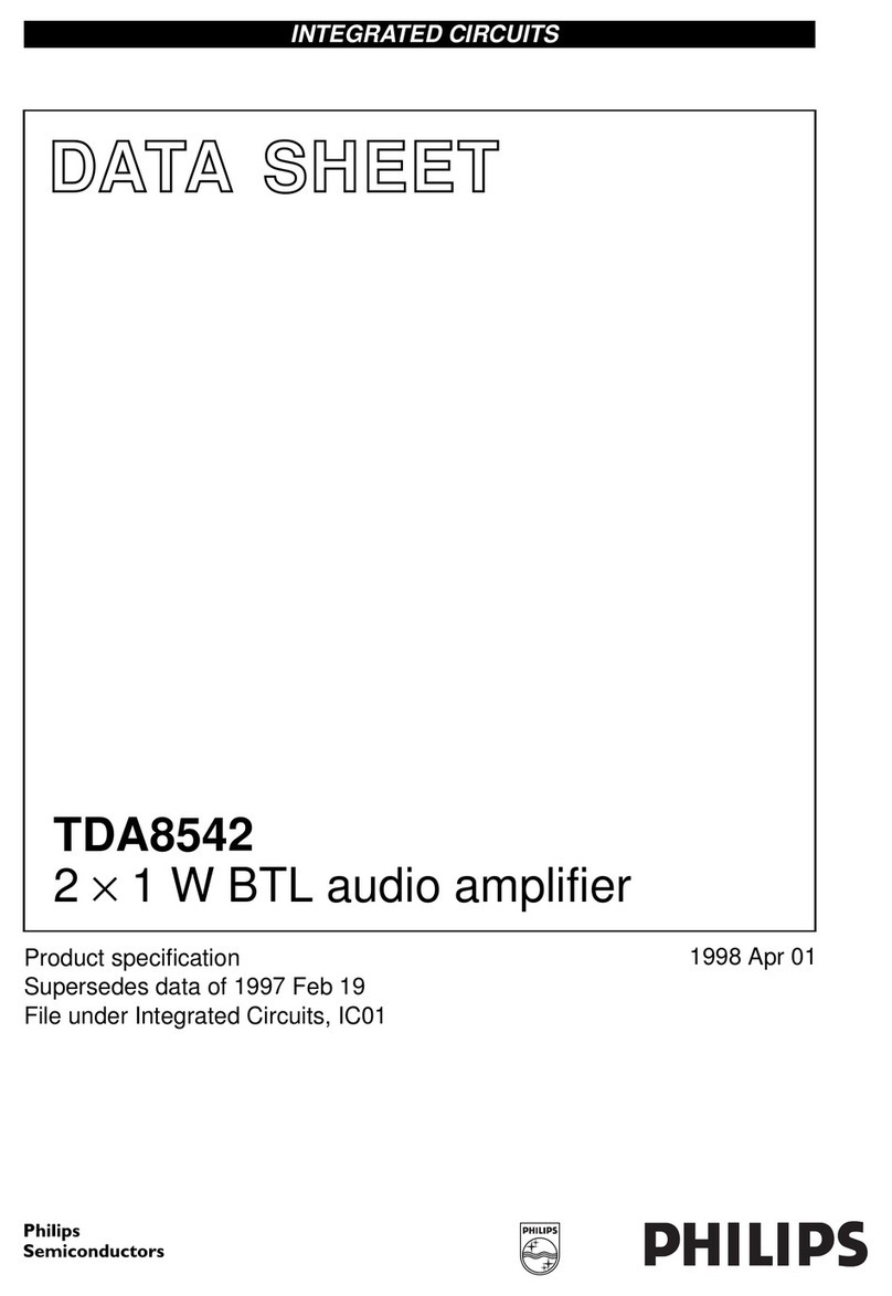
Philips TDA8561Q User manual

DATA SHEET
Product specification
Supersedes data of 1997 Sep 22
File under Integrated Circuits, IC01
1999 Jun 30
INTEGRATED CIRCUITS
TDA8561Q
2×24 W BTL or 4 ×12 W
single-ended car radio power
amplifier

1999 Jun 30 2
Philips Semiconductors Product specification
2×24 W BTL or 4 ×12 W single-ended
car radio power amplifier TDA8561Q
FEATURES
•Requires very few external components
•High output power
•Flexibility in use; Quad single-ended or stereo BTL
•Low output offset voltage
•Fixed gain
•Diagnostic facility (distortion, short-circuit and
temperature detection)
•Good ripple rejection
•Mode select switch (operating, mute and standby)
•Load dump protection
•AC and DC short-circuit safe to ground and to VP
•Low power dissipation in any short-circuit condition
•Thermally protected
•Reverse polarity safe
•Electrostatic discharge protection
•No switch-on/switch-off plop
•Flexible leads
•Low thermal resistance
•Identical inputs (inverting and non-inverting).
GENERAL DESCRIPTION
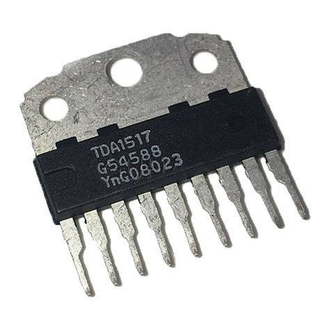
TheTDA8561Qisanintegratedclass-Boutputamplifierin
a 17-lead single-in-line (SIL) power package. It contains
4×12 W Single-Ended (SE) or 2 ×24 W Bridge-Tied
Load (BTL) amplifiers.
The device is primarily developed for car radio
applications.
QUICK REFERENCE DATA
ORDERING INFORMATION
SYMBOL PARAMETER CONDITIONS MIN. TYP. MAX. UNIT
VPpositive operating supply voltage 6 14.4 18 V
IORM repetitive peak output current −−4A
I
Ptotal quiescent current −80 −mA
Isb standby current −0.1 100 µA
Stereo BTL application
Pooutput power RL=4Ω; THD = 10% −24 −W
RR supply voltage ripple rejection 46 −−dB
Vno noise output voltage Rs=0Ω−70 −µV
Z
I
input impedance 25 −−kΩ
∆VO|DC output offset voltage −−150 mV
Quad single-ended application
Pooutput power THD = 10%
RL=4Ω−7−W
R
L
=2Ω−12 −W
RR supply voltage ripple rejection 46 −−dB
Vno noise output voltage Rs=0Ω−50 −µV
Z
I
input impedance 50 −−kΩ
TYPE
NUMBER PACKAGE
NAME DESCRIPTION VERSION
TDA8561Q DBS17P plastic DIL-bent-SIL power package; 17 leads (lead length 12 mm) SOT243-1

1999 Jun 30 3
Philips Semiconductors Product specification
2×24 W BTL or 4 ×12 W single-ended
car radio power amplifier TDA8561Q
BLOCK DIAGRAM
Fig.1 Block diagram.
mode
select
switch
MEA858 - 1
output 1
15 kΩ
15 kΩ
x1
VA
stand-by
switch
VP
mute
switch
stand-by
reference
voltage
513
VP1 VP2
18 kΩ
2
kΩ
mute switch
VA
Cm
power stage
18 kΩ
mute switch
VA
Cm
power stage
6
8
14
18 kΩ
mute switch
VA
Cm
power stage
18 kΩ
mute switch
VA
Cm
power stage
12
10
2711
ground
(signal)
GND1 GND2
power ground (substrate)
output 4
output 3
output 2
non-inverting
input 1
non-inverting
input 4 17
1
TDA8561Q
mute
reference
voltage
input
reference
voltage
2
kΩ
60
kΩ
60
kΩ
inverting
input 2 3
PROTECTIONS
thermal
short-circuit
diagnostic
output
16
4
supply voltage
ripple rejection
inverting
input 3 15
2
kΩ
60
kΩ
2
kΩ
60
kΩ
9
not connected

1999 Jun 30 4
Philips Semiconductors Product specification
2×24 W BTL or 4 ×12 W single-ended
car radio power amplifier TDA8561Q
PINNING
SYMBOL PIN DESCRIPTION
−INV 1 1 non-inverting input 1
GND(S) 2 signal ground
INV 2 3 inverting input 2
RR 4 supply voltage ripple rejection
VP1 5 supply voltage
OUT 1 6 output 1
GND1 7 power ground 1
OUT 2 8 output 2
n.c. 9 not connected
OUT 3 10 output 3
GND2 11 power ground 2
OUT 4 12 output 4
VP2 13 supply voltage
MODE 14 mode select switch input
INV 3 15 inverting input 3
VDIAG 16 diagnostic output
−INV 4 17 non-inverting input 4
Fig.2 Pin configuration.
1
2
3
4
5
6
7
8
9
10
11
12
13
14
15
16
17
TDA8561Q
INV 1
GND(S)
INV 2
RR
OUT 1
GND1
OUT 2
n.c.
OUT 3
GND2
OUT 4
V
MODE
INV 3
DIAG
INV 4
P2
VP1
MEA859 - 1
V

1999 Jun 30 5
Philips Semiconductors Product specification
2×24 W BTL or 4 ×12 W single-ended
car radio power amplifier TDA8561Q
FUNCTIONAL DESCRIPTION
The TDA8561Q contains four identical amplifiers and can
be used for Single-Ended (SE) or Bridge-Tied Load (BTL)
applications. The gain of each amplifier is fixed at 20 dB
(26 dB in BTL). Special features of the device are:
Mode select switch (pin 14)
•Low standby current (<100 µA)
•Low switching current (low cost supply switch)
•Mute facility.
Toavoidswitch-onplops,itisadvised to keep theamplifier
in the mute mode during ≥100 ms (charging of the input
capacitors at pins 1, 3, 15 and 17). This can be achieved
by:
•Microcontroller control
•External timing circuit (see Fig.11).
Diagnostic output (pin 16)
DYNAMIC DISTORTION DETECTOR (DDD)
At the onset of clipping of one or more output stages, the
dynamic distortion detector becomes active and pin 16
goes LOW. This information can be used to drive a sound
processor or DC volume control to attenuate the input
signal and thus limit the distortion. The output level of
pin 16 is independent of the number of channels that are
clipping (see Figs 3 and 4).
SHORT-CIRCUIT PROTECTION
When a short-circuit occurs at one or more outputs to
ground or to the supply voltage, the output stages are
switched off until the short-circuit is removed and the
device is switched on again, with a delay of approximately
20 ms, after removal of the short-circuit. During this
short-circuit condition, pin 16 is continuously LOW.
When a short-circuit across the load of one or both
channels occurs the output stages are switched off for
approximately 20 ms. After that time it is checked during
approximately 50 µs to see whether the short-circuit is still
present. Due to this duty cycle of 50 µs/20 ms the average
current consumption during this short-circuit condition is
very low (approximately 40 mA).
During this short-circuit condition, pin 16 is LOW for 20 ms
and HIGH for 50 µs (see Fig.5).
The power dissipation in any short-circuit condition is very
low.
Fig.3 Distortion detector waveform; BTL
application.
handbook, halfpage
V
0
VP
VO
0
t
MGA705
16
Fig.4 Distortion detector waveform; single-ended
application.
handbook, halfpage
0
VP
VO
t
0
MGA706
V16

1999 Jun 30 6
Philips Semiconductors Product specification
2×24 W BTL or 4 ×12 W single-ended
car radio power amplifier TDA8561Q
TEMPERATURE DETECTION
When the virtual junction temperature Tvj reaches 150 °C, pin 16 will be active LOW.
OPEN-COLLECTOR OUTPUT
Pin 16 is an open-collector output, which allows pin 16 of more devices being tied together.
LIMITING VALUES
In accordance with the Absolute Maximum Rating System (IEC 134).
SYMBOL PARAMETER CONDITIONS MIN. MAX. UNIT
vPpositive supply voltage
operating −18 V
non-operating −30 V
load dump protection during 50 ms; tr≥2.5 ms −45 V
IOSM non-repetitive peak output current −6A
I
ORM repetitive peak output current −4A
T
stg storage temperature −55 +150 °C
Tamb operating ambient temperature −40 +85 °C
Tvj virtual junction temperature −150 °C
Vpsc AC and DC short-circuit safe voltage −18 V
Vpr reverse polarity −6V
P
tot total power dissipation −60 W
Fig.5 Short-circuit waveform.
handbook, full pagewidth
MGL214
short-circuit over the load
20 ms
50 µs
t
t
VP
current
in
output
stage
V16

1999 Jun 30 7
Philips Semiconductors Product specification
2×24 W BTL or 4 ×12 W single-ended
car radio power amplifier TDA8561Q
THERMAL CHARACTERISTICS
In accordance with IEC 747-1.
SYMBOL PARAMETER VALUE UNIT
Rth j-a thermal resistance from junction to ambient in free air 40 K/W
Rth j-c thermal resistance from junction to case (see Figs 6 and 7) 1.3 K/W
Fig.6 Equivalent thermal resistance network;
BTL application.
handbook, halfpage
2.2 K/W
0.2 K/W
2.2 K/W
virtual junction output 1 output 2
case
MEA861 - 1
Fig.7 Equivalent thermal resistance network;
single-ended application.
handbook, halfpage
3.0 K/W
0.7 K/W
3.0 K/W
virtual junction
output 1 output 2
case
3.0 K/W
0.7 K/W
3.0 K/W
output 3 output 4
MEA860 - 2
0.2 K/W

1999 Jun 30 8
Philips Semiconductors Product specification
2×24 W BTL or 4 ×12 W single-ended
car radio power amplifier TDA8561Q
DC CHARACTERISTICS
VP= 14.4 V; Tamb =25°C; measured in Fig.8; unless otherwise specified.
Notes
1. The circuit is DC adjusted at VP= 6 to 18 V and AC operating at VP= 8.5 to 18 V.
2. At18V<V
P< 30 V the DC output voltage ≤0.5VP.
SYMBOL PARAMETER CONDITIONS MIN. TYP. MAX. UNIT
Supply
VPpositive supply voltage note 1 6 14.4 18 V
IPtotal quiescent current −80 160 mA
VODC output voltage note 2 −6.9 −V
∆VODC output offset voltage −−150 mV
Mode select switch
Von switch-on voltage level 8.5 −−V
MUTE CONDITION
Vmute mute voltage 3.3 −6.4 V
VOoutput voltage in mute position VImax = 1 V; f = 1 kHz −−2mV
∆VODC output offset voltage (between
pins 6 to 8 and 10 to 12) −−150 mV
STANDBY CONDITION
Vsb standby voltage 0 −2V
I
sb standby current −−100 µA
Isw switch-on current −12 40 µA
Diagnostic output (pin 16)
VDIAG diagnostic output voltage any short-circuit or clipping −−0.6 V

1999 Jun 30 9
Philips Semiconductors Product specification
2×24 W BTL or 4 ×12 W single-ended
car radio power amplifier TDA8561Q
AC CHARACTERISTICS
VP= 14.4 V; RL=4Ω; f = 1 kHz; Tamb =25°C; unless otherwise specified.
SYMBOL PARAMETER CONDITIONS MIN. TYP. MAX. UNIT
Stereo BTL application (measured in Fig.8)
Pooutput power note 1
THD = 0.5% 15 19 −W
THD = 10% 20 24 −W
THD total harmonic distortion Po=1W −0.06 −%
Pooutput power VP= 13.2 V
THD = 0.5% −16 −W
THD = 10% −20 −W
B power bandwidth THD = 0.5%; −20 to −Hz
Po=−1 dB; with respect to 15 W 15000
fllow frequency roll-off at −1 dB; note 2 −45 −Hz
fhhigh frequency roll-off at −1dB 20 −−kHz
Gvclosed loop voltage gain 25 26 27 dB
SVRR supply voltage ripple rejection note 3
on 48 −−dB
mute 46 −−dB
standby 80 −−dB
ZIinput impedance 25 30 38 kΩ
Vno noise output voltage
on Rs=0Ω; note 4 −70 −µV
on Rs=10kΩ; note 4 −100 200 µV
mute notes 4 and 5 −60 −µV
α
cs channel separation Rs=10kΩ40 60 −dB
∆Gvchannel unbalance −−1dB
DYNAMIC DISTORTION DETECTOR
THD total harmonic distortion V16 ≤0.6 V; no short-circuit −10 −%
Quad single-ended application (measured in Fig.9)
Pooutput power note 1
THD = 0.5% 4 5 −W
THD = 10% 5.5 7 −W
THD total harmonic distortion Po=1W −0.06 −%
POoutput power RL=2Ω; note 1
THD = 0.5% 7.5 10 −W
THD = 10% 10 12 −W
fllow frequency roll-off at −1 dB; note 2 −25 −Hz
fhhigh frequency roll-off at −1dB 20 −−kHz
Gvclosed loop voltage gain 19 20 21 dB

1999 Jun 30 10
Philips Semiconductors Product specification
2×24 W BTL or 4 ×12 W single-ended
car radio power amplifier TDA8561Q
Notes
1. Output power is measured directly at the output pins of the IC.
2. Frequency response externally fixed.
3. Ripple rejection measured at the output with a source impedance of 0 Ω, maximum ripple amplitude of 2 V (p-p) and
at a frequency of between 100 Hz and 10 kHz.
4. Noise measured in a bandwidth of 20 Hz to 20 kHz.
5. Noise output voltage independent of Rs(Vi= 0 V).
SVRR supply voltage ripple rejection note 3
on 48 −−dB
mute 46 −−dB
standby 80 −−dB
ZIinput impedance 50 60 75 kΩ
Vno noise output voltage
on Rs=0Ω; note 4 −50 −µV
on Rs=10kΩ; note 4 −70 100 µV
mute notes 4 and 5 −50 −µV
α
cs channel separation Rs=10kΩ40 60 −dB
∆Gvchannel unbalance −−1dB
DYNAMIC DISTORTION DETECTOR
THD total harmonic distortion V16 ≤0.6 V; no short-circuit −10 −%
SYMBOL PARAMETER CONDITIONS MIN. TYP. MAX. UNIT

1999 Jun 30 11
Philips Semiconductors Product specification
2×24 W BTL or 4 ×12 W single-ended
car radio power amplifier TDA8561Q
TEST AND APPLICATION INFORMATION
Fig.8 Stereo BTL application diagram.
handbook, full pagewidth
MEA862 - 2
100
nF
16 5 13
220 nF 16
8
711
V
P
TDA8561Q
TDA8564Q
2200
µF
60
kΩ
2
ground (signal)
10
kΩ
14
9not connected
3
inverting input 2
60
kΩ
60
kΩ
reference
voltage
220 nF 17 12
60
kΩ
non-inverting
input 4
4
15 10
power ground (substrate)
non- inverting
input 1
supply voltage
ripple rejection
inverting input 3
diagnostic
mode
switch

1999 Jun 30 12
Philips Semiconductors Product specification
2×24 W BTL or 4 ×12 W single-ended
car radio power amplifier TDA8561Q
Fig.9 Quad single-ended application diagram 1.
handbook, full pagewidth
MEA863 - 2
100
nF
16 5 13
220 nF 16
8
711
V
P
TDA8561Q
TDA8564Q
2200
µF
60
kΩ
2
ground (signal)
10
kΩ
14
9not connected
3
inverting
input 2 60
kΩ
60
kΩ
reference
voltage
220 nF
100
µF
17 12
60
kΩ
non-inverting
input 4
4
15 10
power ground (substrate)
non- inverting
input 1
supply voltage
ripple rejection
inverting
input 3
220 nF
1/2Vp
1000 µF
220 nF 1000 µF
1000 µF
1000 µF
mode
switch

1999 Jun 30 13
Philips Semiconductors Product specification
2×24 W BTL or 4 ×12 W single-ended
car radio power amplifier TDA8561Q
Fig.10 Quad single-ended application diagram 2.
(1) When short-circuiting the single-ended capacitor, the dissipation will be reduced due to diode D1.
handbook, full pagewidth
MEA864 - 2
100
nF
16 5 13
220 nF 16
8
711
V
P
V
P
TDA8561Q
TDA8564Q
2200
µF
60
kΩ
2
ground (signal)
10
kΩ
14
4
not connected
3
inverting
input 2
60
kΩ
60
kΩ
reference
voltage
220 nF
17 12
60
kΩ
non-inverting
input 4
9
15 10
power ground (substrate)
non- inverting
input 1
inverting
input 3 220 nF
220 nF
2200
µF
2
D1
100
µF
mode
switch

1999 Jun 30 14
Philips Semiconductors Product specification
2×24 W BTL or 4 ×12 W single-ended
car radio power amplifier TDA8561Q
Mode select switch
Toavoid switch-on plops, itisadvised to keep theamplifier
in the mute mode during >100 ms (charging of the input
capacitors at pins 1, 3, 15 and 17.
The circuit in Fig.11 slowly ramps up the voltage at the
mode select switch pin when switching on and results in
fast muting when switching off.
Fig.11 Mode select switch circuitry.
handbook, halfpage
100 kΩ
MGA708
47 µF
10 kΩ100 Ω
mode
select
switch
VP
Fig.12 Total harmonic distortion as a function of output power; VP= 14.4 V, RL=4Ω.
(1) f = 10 kHz.
(2) f = 1 kHz.
(3) f = 100 Hz.
102
MGA709
10110 1
102
10
1
10
P (W)
o
10 2
1
10 2
THD
(%)
(1)
(2)
(3)

1999 Jun 30 15
Philips Semiconductors Product specification
2×24 W BTL or 4 ×12 W single-ended
car radio power amplifier TDA8561Q
handbook, full pagewidth
18
50
0810121416
MGA710
10
20
30
40
Po
(W)
V (V)
P
(1)
(3)
(2)
Fig.13 Output power as a function of supply voltage.
(1) THD = 30%.
(2) THD = 10%.
(3) THD = 0.5%.
Fig.14 Power bandwidth as a function of frequency; THD = 0.5%, VP= 14.4 V, RL=4Ω.
10
20
105
MGA711
104
103
102
10
12
14
16
18
f (Hz)
Po
(W)

1999 Jun 30 16
Philips Semiconductors Product specification
2×24 W BTL or 4 ×12 W single-ended
car radio power amplifier TDA8561Q
Fig.15 Total harmonic distortion as a function of frequency; VP= 14.4 V, RL=4Ω.
(1) Po= 0.1 W.
(2) Po=1W.
(3) Po=10W.
105
MGA712
104
103
102
10
1
10 2f (Hz)
10 1
THD
(%)
(1)
(2)
(3)
100
50
105
MGA713
104
103
102
10
90
80
70
60
f (Hz)
RR
(dB) (1)
(2)
(3)
Fig.16 Ripple rejection as a function of frequency.
(1) On condition.
(2) Mute condition.
(3) Standby condition.

1999 Jun 30 17
Philips Semiconductors Product specification
2×24 W BTL or 4 ×12 W single-ended
car radio power amplifier TDA8561Q
Fig.17 Quiescent current as a function of supply voltage; RL=∞.
handbook, full pagewidth
18
100
60 8 10121416
MGA714
68
76
84
92
V (V)
P
Iq
(mA)
SINGLE-ENDED APPLICATION
102
MGA715
10110 1
102
10
1
10
P (W)
o
10 2
1
10 2
THD
(%)
(2)
(1)
(3)
Fig.18 Total harmonic distortion as a function of output power; VP= 14.4 V, RL=2Ω.
(1) f = 10 kHz. (2) f = 1 kHz. (3) f = 100 Hz.

1999 Jun 30 18
Philips Semiconductors Product specification
2×24 W BTL or 4 ×12 W single-ended
car radio power amplifier TDA8561Q
Fig.19 Output power as a function of supply voltage.
(1) THD = 30%.
(2) THD = 10%.
(3) THD = 0.5%.
handbook, full pagewidth
18
15
08 10121416
MGA716
3
6
9
12
Po
(W)
V (V)
P
(2)
(3)
(1)
Fig.20 Power bandwidth as a function of frequency; THD = 0.5%, VP= 14.4 V, RL=2Ω.
0
10
105
MGA717
104
103
102
10
2
4
6
8
f (Hz)
Po
(W)

1999 Jun 30 19
Philips Semiconductors Product specification
2×24 W BTL or 4 ×12 W single-ended
car radio power amplifier TDA8561Q
Fig.21 Total harmonic distortion as a function of frequency; VP= 14.4 V, RL=2Ω.
(1) Po= 0.1 W.
(2) Po=1W.
105
MGA718
104
103
102
10
1
10 2f (Hz)
10 1
THD
(%)
(1) (2)
Fig.22 Channel separation as a function of frequency.
handbook, full pagewidth
80
30
105
MGA719
104
103
102
10
70
60
50
40
f (Hz)
(dB)
αcs

1999 Jun 30 20
Philips Semiconductors Product specification
2×24 W BTL or 4 ×12 W single-ended
car radio power amplifier TDA8561Q
BTL APPLICATION
Fig.23 Total power dissipation as a function of output power; VP= 14.4 V, RL=4Ω(1 channel driven BTL or
4 channels in single-ended mode).
14
204
MGA720
4
Ptot
(W)
P (W)
o
6
8
10
12
8 1216202428
Table of contents
Other Philips Amplifier manuals

Philips
Philips TDA5360 User manual

Philips
Philips Amplifier User manual

Philips
Philips PM 3344 User manual

Philips
Philips CMQ405 User manual

Philips
Philips TDA8586 User manual

Philips
Philips TDA2549 User manual

Philips
Philips SWV2116 User manual

Philips
Philips BGY148A User manual

Philips
Philips FA 950 User manual

Philips
Philips TDA1597 User manual

Philips
Philips FA 911 User manual

Philips
Philips 5534A User manual

Philips
Philips BGY88 User manual

Philips
Philips BGY1916 User manual

Philips
Philips FA741/00 User manual

Philips
Philips NE5205A User manual

Philips
Philips TDA8922 User manual

Philips
Philips TDA1562Q User manual

Philips
Philips FA 931 User manual

Philips
Philips BGY685AL User manual