2
1234
1234
C
D
F
A
B
E
DV-355
1. CONTRAST OF MISCELLANEOUS PARTS
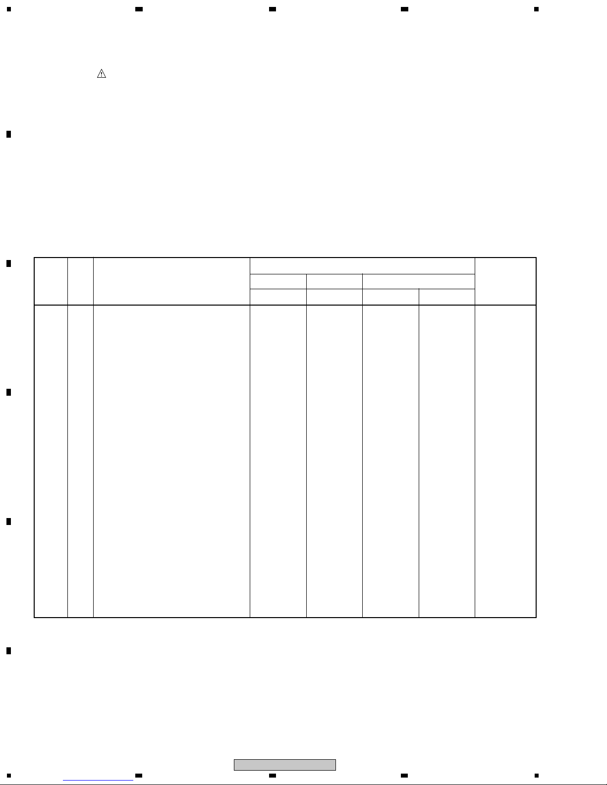
7CONTRAST TABLE for DV-355 and DV-355-K
DV-355/RDXU/RA, DV-355-K/RDXU/RBNC, RPWXU and DV-250/KUXU are constructed the same except for the
following:
PCB ASSEMBLIES
P9 - 3 FJMB ASSY VWS1515 VWS1522 VWS1522 VWS1522
P9 - 7 >POWER SUPPLY Unit VWR1351 VWR1352 VWR1352 VWR1352
(or VWR1353) (or VWR1354) (or VWR1354) (or VWR1354)
PACKING
P7 - 1 >Power Cable ADG7022 ADG1158 ADG1158 Not used
P7 - 2 NSP Warranty Card ARY7057 ARY7025 Not used Not used
P7 - 5 Operating Instructions (English) VRB1285 VRB1287 VRB1287 VRB1287
P7 -11 Paper Board VHC1089 VHC1089 VHC1089 Not used
P7 -12 Packing Case VHG2158 VHG2189 VHG2190 VHG2199
Operating Instructions (Arabic) Not used Not used VRC1151 Not used
>Power Cable Not used Not used Not used ADG1160 No. 1
Accessory Box Not used Not used Not used VHC1092 No. 2
EXTERIOR SECTION
P9 -13 Rear Panel VNA2435 VNA2423 VNA2424 VNA2444
P9 -18 Tray Panel VNK4959 VNK4974 VNK4974 VNK4974
P9 -19 Front Panel Assy VXA2490 VXA2511 VXA2511 VXA2511
P9 -20 Pioneer Badge VAM1129 VAM1130 VAM1130 VAM1130
P9 -21 NSP Energy Star Label AAX7876 Not used Not used AAX7876
P9 -26 Bonnet Case S VXX2830 VXX2831 VXX2831 VXX2831
NSP Caution Label E VRW1935 Not used Not used Not used
NSP Caution Label F VRW1936 Not used Not used Not used
Label Not used VRW1872 VRW1872 VRW1872 for Bonnet
Remarks
Part No.
DV-250 DV-355 DV-355-K
KUXU RDXU/RA RDXU/RBNC RPWXU
Ref.
No. Mark Symbol and Description
NOTES : ÷Parts marked by “ NSP ” are generally unavailable because they are not in our Master Spare Parts List.
÷The mark found on some component parts indicates the importance of the safety factor of the part.
Therefore, when replacing, be sure to use parts of identical designation.
÷Reference Nos. indicate the pages and Nos. in the service manual for the base model.
÷When ordering resistors, first convert resistance values into code form as shown in the following examples.
Ex. 1 When there are 2 effective digits (any digit apart from 0), such as 560 ohm and 47k ohm (tolerance is shown by
J = 5%, and K = 10%).
560 Ω=56 ×10 1 =561 ................................................... RD1/4PU 561J
47k Ω=47 ×10 3=473 .................................................. RD1/4PU 473J
0.5 Ω=R50 ...................................................................... RN2H Â50K
1 Ω=1R0 ......................................................................... RS1P 1Â0K
Ex. 2 When there are 3 effective digits (such as in high precision metal film resistors).
5.62k Ω=562 ×10 1=5621 ........................................... RN1/4PC 5621F
•The numbers in the remarks column correspond to the numbers on the “EXPLODED VIEWS”.
•For PCB assemblies, Refer to “CONTRAST OF PCB ASSEMBLIES”, “PCB PARTS LIST”, “2. SCHEMATIC DIAGRAM” and “3. PCB CONNECTION
DIAGRAM”.


