Power One H Series User manual

CassetteStyle AC-DC Converters HSeries
Edition1/04.2002 1/20
70 Watt AC-DC Converters H Series
• Universal input voltage range suitable for most AC
mains
• Efficient input filter and built-in surge and transient
suppression circuitry
• Outputs individually isolated
• Outputs fully protected against overload
Table of Contents Page
Summary.......................................................................... 1
Type Survey and Key Data .............................................. 2
Type Key .......................................................................... 2
Functional Description...................................................... 3
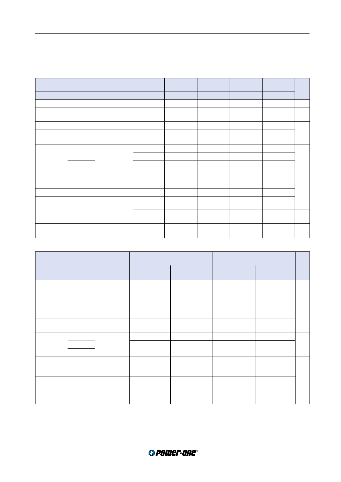
Electrical Input Data ......................................................... 4
Electrical Output Data ...................................................... 5
Auxiliary Functions ........................................................... 8
Summary
The H series of AC-DC converters represents a flexible
range of power supplies for use in advanced electronic sys-
tems. Features include high efficiency, reliability and low
output voltage noise.
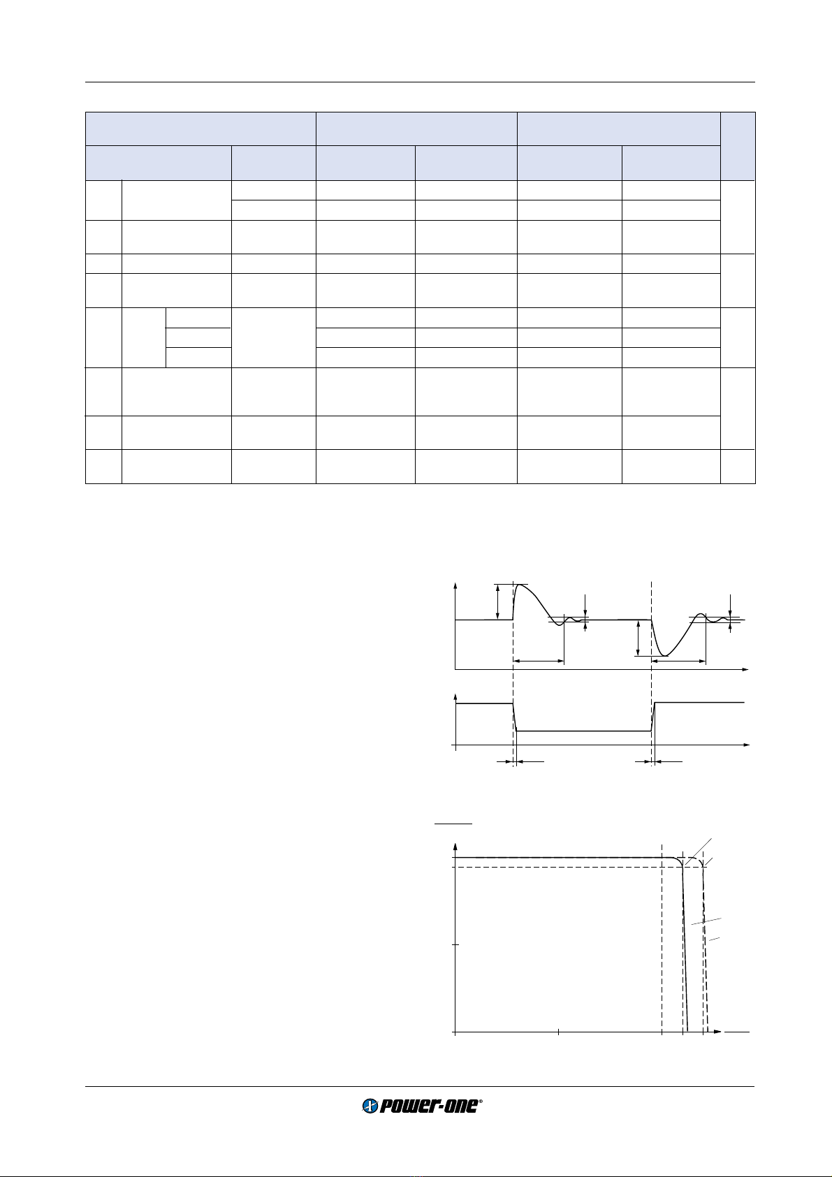
The converter inputs are protected against surges and tran-
sients occuring at the source lines. An input over- and
undervoltage lock-out circuitry disables the outputs if the
input voltage is outside the specified range. The modules
include an inrush current limitation preventing circuit break-
ers and fuses from being damaged at switch-on.
All outputs are open- and short-circuit proof and are pro-
tectedagainstovervoltages by meansof built-in suppressor
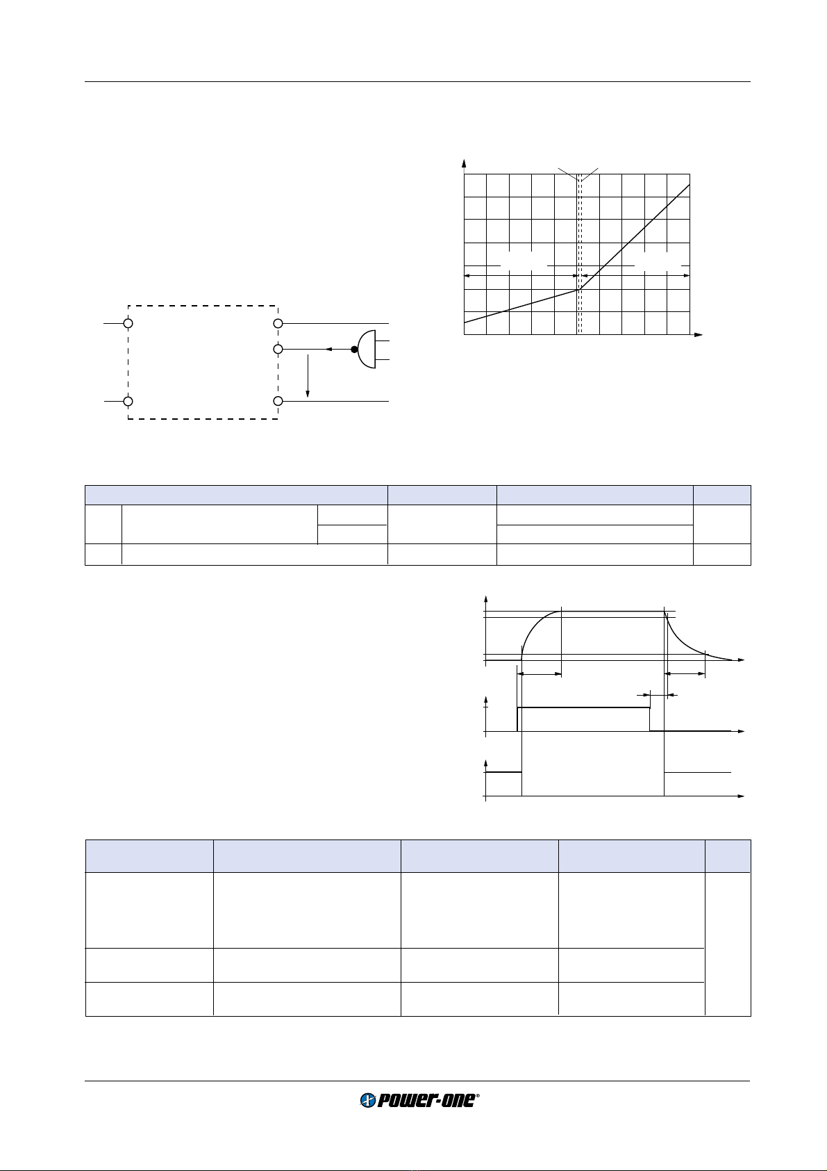
diodes. The outputs can be inhibited by a logic signal ap-
plied to the connector pin 2 (i). If the inhibit function is not
used pin 2 should be connected to pin 23 to enable the out-
puts.
LED indicators display the status of the converter and allow
visual monitoring of the system at any time.
Full input to output, input to case, output to case and output
to output isolation is provided. The modules are designed
and built according to the international safety standard IEC/
EN 60950 and have been approved by the safety agencies
LGA (Germany) and UL (USA). The UL Mark for Canada
has been officially recognized by regulatory authorities in
provinces across Canada.
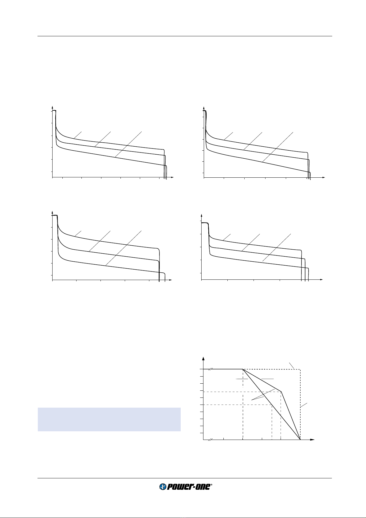
The case design allows operation at nominal load up to
50°C in a free air ambient temperature. If forced cooling is
provided, the ambient temperature may exceed 50°C but
the case temperature should remain below 80°C under all
conditions. Applying a derating factor, operation above
50°C with reduced output power is possible.
A temperature sensor generates an inhibit signal which
disablestheoutputs if thecase temperature
T
Cexceedsthe
limit. The outputs are automatically re-enabled when the
temperature drops below the limit.
Two different options are available to adapt the converters
to individual applications (D, V).
The modules may either be plugged into 19" rack systems
according to DIN 41494, or be chassis mounted.
Important: These products are intended to replace the
110H and the 230H units.
Safety according to IEC/EN 60950
168
6.6"
39
1.54"
8TE
111
4.37"
3U
Page
Electromagnetic Compatibility (EMC) ............................ 10
Immunity to Environmental Conditions........................... 11
Mechanical Data ............................................................ 12
Safety and Installation Instructions ................................ 13
Description of Options.................................................... 16
Accessories.................................................................... 20
Input voltage range 85...255 V AC
1, 2 or 3 isolated outputs up to 48 V DC
Class I equipment
LGA

CassetteStyle AC-DC Converters HSeries
Edition1/04.2002 2/20
Type Key
Type Key L H 2 5 40 -2 R D V
Input voltage range
U
i:
85...255 V AC .............................................. L
Series .............................................................................. H
Number of outputs....................................................... 1...3
Output 1,
U
o1 nom:
5.1 V ............................................................ 0
12 V ............................................................. 3
15 V ............................................................. 5
24 V ............................................................. 6
48 V ............................................................. 9
Single output modules ................................................... 01
Output 2 and 3,
U
o2 nom,
U
o3 nom:
12 V ........................................................... 20
15 V ........................................................... 40
Options and features:
Ambient temperature range
T
A:
–10...50°C...................................................-2
Output voltage control input
(single output modules only)....................... R
Save data signal (D1...D8, to be specified) D 1
ACFAIL signal (V2, V3, to be specified).......V 1, 2
1Option D excludes option V and vice versa
2Option V only for modules with
U
o1 = 5.1 V
Type Survey and Key Data
Table 1: Type survey
Output 1 Output 2 Output 3 Input Voltage Range and Efficiency1 Options
U
o nom
I
o nom
U
o nom
I
o nom
U
o nom
I
o nom
U
i min...
U
i max hmin
[V DC] [A] [V DC] [A] [V DC] [A] 85...255 VAC/47...63 Hz [%]
5.1 11 - - - - LH1001-2R 74 V2, V3 2
12.0 6 - - - - LH1301-2R 81 D1...D8
15.0 4.5 - - - - LH1501-2R 83
24.0 3 - - - - LH1601-2R 83
48.0 1.5 - - - - LH1901-2R 83
12.0 2.0 12.03 2.0 - - LH2320-2 81
15.0 1.7 15.03 1.7 - - LH2540-2 81
5.1 5.0 12.03 0.7 12.03 0.7 LH3020-2 78
5.1 5.0 15.03 0.6 15.03 0.6 LH3040-2 78
1 Efficiency at
U
i nom and
I
o nom.
2 Option V only for modules with
U
o1 = 5.1 V.
3 Outputs 2 and 3 unregulated.
Example: LH1501-2RD3: AC-DC converter, input voltage range 85...255 V AC, providing one output with
15 V/4.5 A, equipped with an output voltage control input (R) and undervoltage monitoring (D3).

CassetteStyle AC-DC Converters HSeries
Edition1/04.2002 3/20
Fig. 1
AC-DC converter block diagram
Input filter
Current
limitation
output 3
Main control circuit
Current
limitation
output 2
29
11
8
23
5
26
32
17
14
20
2
Forward converter
approx. 70 kHz
4
4
Y
Y
Y Y
14
17
i
D/V
R
G
N
P
2
3
03084
1
Functional Description
The input voltage is fed via an input fuse, an input filter, an
inrush current limiter and a rectifier to the input capacitor.
This capacitor sources a single transistor forward con-
verter. Each output is powered by a separate secondary
winding of the main transformer. The resulting voltages are
rectified and their ripples smoothed by a power choke. The
control logic senses the main output voltage
U
o1 and gener-
ates, with respect to the maximum admissible output cur-
rents, the control signal for the primary switching transistor.
This signal is fed back via a coupling transformer.
The auxiliary outputs
U
o2 and
U
o3 are unregulated. Each
auxiliary output's current is sensed and transferred to the
main control circuit using a current transformer. If one of the
outputs is driven into current limit, the other outputs will re-
duce their output voltages as well because all output cur-
rents are controlled by the same control circuit.
1Input fuse
2Transient suppressor (VDR)
3Inrush current limiter (NTC)
4R input for LH 1000

CassetteStyle AC-DC Converters HSeries
Edition1/04.2002 4/20
Electrical Input Data
General conditions:
–
T
A= 25°C, unless
T
Cis specified.
–Connector pins 2 and 23 interconnected, R input not connected.
Table 2: Input data
Input LH
Characteristics Conditions min typ max Unit
U
iOperating input voltage
I
o= 0…
I
o nom 85 255 V AC
U
i nom Nominal input voltage
T
C min…
T
C max 230
I
iInput current
U
i nom,
I
o nom 1 0.44 Arms
P
i 0 No-load input power:
U
i nom W
Single output
I
o1,2,3 = 0 1 2.5
Double output 7 9
Triple output 7 9
P
i inh Idle input power inhibit mode 2.5
I
inr p 3 Peak inrush current
U
i
=
U
i max 42 A
t
inr r Rise time
R
S= 0 Ω 4300 µs
t
inr h Time to half-value
T
C= 25°C1600
R
iInput resistance
T
C= 25°C 800 mΩ
R
NTC 2 NTC resistance 8000
C
iInput capacitance 140 270 µF
U
I RFI Cond. Input RFI EN 55022 A
EI RFI Rad. Input RFI
U
i nom,
I
o nom B
U
i abs Input voltage limits 0 284 V AC
without any damage
1With multiple output modules, all outputs, loadad with
I
o nom.
2Initial switch-on cycle. Subsequent switch on/off cycles increase the inrush current peak value.
3
I
inr p
=
U
i/(
R
s
+
R
i+
R
NTC)
4
R
S= source resistance.
Input fuse
A fuse mounted inside the module protects the module
against severe defects. If operated from a DC source this
fuse may not fully protect the module when the input volt-
age exceeds 200 V DC! In applications where the convert-
ers operate at source voltages above 200 V DC an external
fuse or circuit breaker at system level should be installed.
Table 3: Fuse specification
Series Fuse type Fuse rating
LH slow blow SPT 2.5 A, 250 V
Input Under-/Overvoltage Lock-out
If the input voltage remains below approx. 60 V AC or ex-
ceeds approx. 280 VAC, an internally generated inhibit sig-
nal disables the output(s). When checking this function the
absolute maximum input voltage rating
U
i abs must be care-
fully considered (see table:
Input data
). Between
U
i min and
the undervoltage lock-out level the output voltage may be
below the value defined in table:
Output data
(see:
Techni-
cal Information: Measuring and Testing
).
Input Transient Protection
A VDR together with the input fuse and a symetrical input
filterforman effectiveprotection against highinput transient
voltages.
Inrush Current Limitation
The modules incorporate an NTC resistor in the input cir-
cuitry which –at initial turn on –reduces the peak inrush
current value by a factor of 5...10 to protect connectors and
switching devices from damage. Subsequent switch-on cy-
cles within short periods will cause an increase of the peak
inrush current value due to the warming-up of the NTC re-
sistor.
Inrush Current Peak Value
The inrush current peak value (initial switch-on cycle) can
be determined by the following calculation:
U
i rms •√2
I
inr p = –––––––––––––––
(
R
s ext +
R
i+
R
NTC)
R
s ext
R
i
R
NTC
I
inr p
U
i rms
C
i
04001
Fig. 2
Equivalent circuit diagram for input impedance.

CassetteStyle AC-DC Converters HSeries
Edition1/04.2002 5/20
Electrical Output Data
General conditions
–
T
A= 25°C, unless
T
Cis specified.
–Connector pins 2 and 23 interconnected, R input not connected.
Table 4a: Output data
Output LH 1001 LH 1301 LH 1501 LH 1601 LH 1901
5.1 V 12 V 15 V 24 V 48 V
Characteristics Conditions min typ max min typ max min typ max min typ max min typ max Unit
U
oOutput voltage
U
i nom,
I
o nom 5 5.20 11.76 12.24 14.70 15.30 23.52 24.48 47.04 48.96 V
U
o p Output overvoltage 7.5 21 25 41 85
protection
I
o nom Output current1 0 11 0 6 0 4.5 0 3 0 1.5 A
I
o L Output current limit 2
U
i min...
U
i max 11.44 6.24 4.68 3.12 1.56
T
C min...
T
C max
u
oOutput Low freq.
U
i nom,
I
o nom 1 5 610 510 410 210mV
pp
voltage Switch. freq. IEC/EN 612046 30 50 60 100 50 80 30 50 20 40
noise Total BW = 20 MHz 60 200 70 200 75 200 75 200 35 150
D
U
o U Static line regulation
U
i min...
U
i nom ±50 ±100 ±100 ±150 ±150 mV
U
i nom...
U
i max
I
o nom
D
U
o I Static load regulation
U
i nom,
I
o nom...0 50 150 150 150 150
u
o d 4Dynamic Voltage
U
i nom ±200 ±400 ±200 ±200 ±150
load deviation
I
o nom ↔ 1/2
I
o nom
t
d 4regulation Recovery IEC/EN 61204 100 80 80 80 120 µs
time
aUo Temperature
U
i min...
U
i max ±1.0 ±2.4 ±3.0 ±4.8 ±9.6 mV/K
coefficient D
U
o/D
T
C0...
I
o nom
1If the output voltage is increased above
U
o nom through R input
control, the output current should be reduced accordingly so
that
P
o nom is not exceeded.
2See fig.:
Output voltage U
o1
versus output currents.
3Measured according to IEC/EN 61204 sub clause 3.10 with a
Table 4b: Output data
Output LH 2320 LH 2540
2 x 12 V 2 x 15 V
Characteristics Conditions Output 1 Output 2 Output 1 Output 2
min typ max min typ max min typ max min typ max Unit
U
oOutput voltage
U
i nom,
I
o nom 11.76 12.24 11.40 12.60 14.70 15.30 14.25 15.75 V
U
i nom,
I
o2/3 = 0 –13.80 –17.25
U
o p Output overvoltage 21 25 25 31
protection
I
o nom Output current 0 2 0 2 0 1.7 0 1.7 A
I
o L Output current limit 2
U
i min...
U
i max 2.08 2.08 1.77 1.77
T
C min...
T
C max
u
o3 Output Low freq.
U
i nom,
I
o nom 1 5 1 5 0.5 5 0.5 5 mVpp
voltage Switch. freq. IEC/EN 612046 15 30 20 40 15 30 20 40
noise Total BW = 20 MHz 50 150 50 150 40 150 40 150
D
U
o U Static line regulation
U
i min...
U
i nom ±50 ±80 ±60 ±80 mV
U
i nom...
U
i max
I
o nom
D
U
o I Static load regulation
U
i nom 50
see: LH2320-2:
60
see: LH2540-2:
I
o nom...05
D
U
o2
(typ.) vs. I
o2
D
U
o2
(typ.) vs. I
o2
aUo Temperature
U
i min...
U
i max ±2.4 ±3.0 mV/K
coefficient D
U
o/D
T
C0...
I
o nom
probe according to annex. A of the same standards.
4See fig.:
Dynamic load regulation of U
o1.
5Condition for specified output. Other output(s) loaded with con-
stant current
I
o=
I
o nom.
6See:
Technical Information: Measuring and Testing.

CassetteStyle AC-DC Converters HSeries
Edition1/04.2002 6/20
Table 4c: Output data
Output LH 3020 LH 3040
5.1 V, 2 x 12 V 5.1 V, 2 x 15 V
Characteristics Conditions Output 1 Output 2/3 Output 1 Output 2/3
min typ max min typ max min typ max min typ max Unit
U
oOutput voltage
U
i nom,
I
o nom 5.00 5.20 11.40 12.60 5.00 5.20 14.25 15.75 V
U
i nom,
I
o2/3 = 0 –13.80 –17.25
U
o P Output overvoltage 7.5 25 7.5 31
protection
I
o nom Output current 0 5 0 0.7 0 5 0 0.6 A
I
o L Output current limit 2
U
i min...
U
i max 5.20 0.73 5.20 0.62
T
C min...
T
C max
u
o3 Output Low freq.
U
i nom,
I
o nom 1 5 0.5 5 1 5 0.5 5 mVpp
voltage Switch. freq. IEC/EN 612046 15 30 10 20 15 30 10 20
noise Total BW = 20 MHz 30 150 20 150 30 150 40 150
D
U
o U Static line regulation
U
i min...
U
i nom ±30 ±150 ±30 ±150 mV
U
i nom...
U
i max
I
o nom
D
U
o I Static load regulation
U
i nom 25
see: LH3020-2:
25
see: LH3040-2:
I
o nom...05 D
U
o2
(typ.) vs. I
o2 D
U
o2
(typ.) vs. I
o2
aUo Temperature
U
i min...
U
i max ±1.0 ±1.0 mV/K
coefficient D
U
o/D
T
C0...
I
o nom
Parallel and series connection
Parallel connection of main outputs
The main outputs from any modules with equal nominal
voltage can be connected in parallel. It is important to as-
sure that the main output of a multiple output module is
forced to supply a minimum current of approx. 10% of
I
o nom
to enable correct operation of its own auxiliary output(s). In
parallel operation, one or more of the outputs may operate
continuously in current limit which will cause an increase in
case temperature. Consequently, a reduction of the max.
ambient temperature by 10 K is recommended.
Parallel connection of the outputs from a double output
module (LH2320/2540)
Output one and two of the same double output module can
be connected in parallel without a minimum current require-
ment at the main output.
Parallel connection of the auxiliary outputs from a triple out-
put module (LH 3020/3040)
Output two and three of the same triple output module can
be connected in parallel, if the outputs are decoupled with
diodes or the minimum current is ≥10% of
I
o nom.
Note: Auxiliary outputs from different modules may not be
connected in parallel.
Series connection
Main or auxiliary outputs can be connected in series with
any other output of the same or another module. In series
connection, the maximum output current is limited by the
output with the lowest current limitation. Output ripple and
regulation values are added. Connection wiring should be
kept as short as possible. If ouput terminals are connected
together in order to establish multi-voltage configurations,
e.g.+5.1V,±12 V etc.thecommon ground connectingpoint
should be as close as possible to the connector of the con-
verter to avoid excessive output ripple voltages.
I
o1/
I
o1 nom
1
u
o1d
u
o1d
t
d
t
d
D
U
r
D
U
r
t
U
o
0
t
<10 µs
<10 µs
05131
0.5
Fig. 3
Control deviation of U
o1
d vs. dynamic load change
1.0
0
0.5
U
o1
0.5
U
o1 nom
I
o
I
o nom
1.0 1.2
I
o nom
I
o1
I
o2
,
I
o3
I
oL1
I
oL2
,I
oL3
.95
05022
Fig. 4
Typical output voltage U
o1
versus output currents I
o.
1If the output voltage is increased above
U
o nom through R input
control, the output current should be reduced accordingly so
that
P
o nom is not exceeded.
2See fig.
Output voltage U
o1
versus output currents.
3Measured according to IEC/EN 61204 sub clause 3.10 with a
probe according to annex. A of the same standards.
4See fig.:
Dynamic load regulation of U
o1.
5Condition for specified output. Other output(s) loaded with con-
stant current
I
o=
I
o nom.
6See:
Technical Information: Measuring and Testing.

CassetteStyle AC-DC Converters HSeries
Edition1/04.2002 7/20
Fig. 5
LH2320-2:
D
U
o2
(typ.) vs. I
o2
with different I
o1.
U
i= 230 V AC
Output Protection
Each output is protected against overvoltages which could
occur due to a failure of the internal control circuit. Voltage
suppressor diodes (which under worst case condition may
become a short circuit) provide the required protection. The
suppressor diodes are not designed to withstand externally
applied overvoltages. Overload at any of the outputs will
cause a shut-down of all outputs.
I
o1
= 0%
11.0
11.5
12.0
12.5
13.0
13.5
0.2 0.6 1.0 1.4
0
I
o1
= 100% I
o1
= 50%
U
o2
[V]
I
o2
[A]
1.8 2.2
05133
14.0
14.5
15.0
16.0
16.5
0.4 0.8 1.6
0
I
o1
= 100% I
o1
= 50%
U
o2
[V]
I
o2
[A]
05135
I
o1
= 0%
1.2 2.0
15.5
11.0
11.5
12.0
12.5
13.0
13.5
0.2 0.4 0.6 0.8
0
I
o1
= 100% I
o1
= 50% I
o1
= 0%
U
o2/3
[V]
I
o2/3
[A]
05132
13
14
15
16
17
0.2 0.4 0.6
0
I
o1
= 100% I
o1
= 50%
U
o2/3
[V]
I
o2/3
[A]
05134
I
o1
= 0%
Fig. 6
LH2540-2:
D
U
o2
(typ.) vs. I
o2
with different I
o1.
U
i= 230 V AC
Fig. 7
LH3020-2:
D
U
o2/3
(typ.) vs.I
o2/3
with different I
o1.
U
i= 230 V AC
Fig. 8
LH3040-2:
D
U
o2/3
(typ.) vs. I
o2/3
with different I
o1.
U
i= 230 V AC
Thermal Considerations
If a converter is located in free, quasi-stationary air (con-
vection cooling) at the indicated maximum ambient tem-
perature
T
Amax (see table:
Temperature specifications)
and
is operated at its nominal input voltage and output power,
the temperature measured at the
Measuring point of case
temperature T
C
(see:
Mechanical Data
) will approach the
indicated value
T
C max after the warm-up phase. However,
the relationship between
T
Aand
T
Cdepends heavily on the
conditions of operation and integration into a system. The
thermal conditions are influenced by input voltage, output
current, airflow and temperature of surrounding compo-
nents and surfaces.
T
A max is therefore, contrary to
T
C max,
an indicative value only.
Caution: The installer must ensure that under all operat-
ing conditions
T
Cremains within the limits stated in the
table:
Temperature specifications.
Notes: Sufficient forced cooling or an additional heat sink
allows
T
Ato be higher than 50°C (e.g. 65°C) if
T
C max is not
exceeded.
At an ambient temperature
T
Aof 65°C with only convection
cooling,themaximum permissible currentfor each outputis
approx. 50% of its nominal value as per figure.
0
0.1
0.2
0.3
0.4
0.5
0.6
0.7
0.8
40 60 70 80
I
o
/I
o nom
T
A
[°C]
0.9
1.0 Forced cooling
05142
T
C max
50
Convection cooling
T
A min
LH 2000
LH 3000 LH 1000
Fig. 9
Output current derating versus temperature
Thermal Protection
A temperature sensor generates an internal inhibit signal
which disables the outputs if the case temperature exceeds
T
C max. The outputs are automatically reenabled if the tem-
perature drops below this limit.
Output voltage regulation of multiple output modules
Output 1 is under normal conditions regulated to
U
o1 nom,
independent of the output current.
U
o2 and
U
o3 are unregu-
lated and depend upon their own load and the load on out-
put 1.

CassetteStyle AC-DC Converters HSeries
Edition1/04.2002 8/20
Output Response
The reaction of the outputs is similar whether the input volt-
age is applied or the inhibit is switched low.
An output voltage overshoot will not occur when the module
is turned on or off.
Fig. 12
Output response as a function of input voltage (on/off
switching) or inhibit control
Table 6: Output response time trand tf
Type of Converter
t
rat
P
o = 0 and
t
fat
P
o =
P
o nom
t
rand
t
fat
P
o =3/4
P
o nom
t
rat
P
o =
P
o nom Unit
typ max typ max typ max
LH1001-2R 3 17 3 17 5 25 ms
LH1301-2R 5 25 8 30 10 40
LH1501-2R 3 17 5 25 15 50
LH1601-2R 8 30 15 45 20 70
LH1901-2R 35 100 50 150 85 230
LH2320-2 10 40 15 50 25 80
LH2540-2 8 30 10 40 20 60
LH3020-2 30 85 45 130 75 210
LH3040-2 20 70 30 90 50 150
Conditions:
R input not used. For multiple output modules the figures indicated in the table above relate to the output which reacts
slowest. All outputs are resistively loaded. Variation of the input voltage within
U
i min...
U
i max does not influence the values.
0t
r
t
f
t
t
0
Inhibit
1
Output
0.1
U
o nom
t
0
1
0.95U
o nom
t
h
U
i
05025
Auxiliary Functions
i Inhibit for Remote On and Off
Note: With open i input: Output is disabled (
U
o= off).
The outputs of the module may be enabled or disabled by
means of a logic signal (TTL, CMOS, etc.) applied between
the inhibit input i and the negative pin of output 1 (Vo1–). In
systems with several units, this feature can be used, for ex-
ample, to control the activation sequence of the converters.
Iftheinhibit function is notrequired, connect the inhibitpin2
to pin 23 to enable the outputs (active low logic, fail safe).
For output response refer to:
Hold-up Time and Output Re-
sponse
.
Vi~
Vi~ Vo–
i
Vo+ I
inh
U
inh
06115
1.6
0.8
0
–0.8
–50
U
inh
[V]
I
inh
[mA]
–30 0–10 10 30 50
2.0
1.2
0.4
–0.4
U
inh
= 0.8 V
U
o
= on
U
o
= off
U
inh
= 2.4 V
06032
Fig. 10
Definition of U
inh
and I
inh
.
Fig. 11
Typical inhibit current I
inh
versus inhibit voltage U
inh
Table 5: Inhibit data
Characteristics Conditions min typ max Unit
U
inh Inhibit input voltage to keep
U
o= on
U
i min...
U
i max –50 0.8 V DC
output voltage
U
o= off
T
C min...
T
C max 2.4 50
I
inh Inhibit current
U
inh = 0 –60 –100 –220 µA

CassetteStyle AC-DC Converters HSeries
Edition1/04.2002 9/20
R-Control for Output Voltage Adjustment
Note: With open R input,
U
o ≈
U
o nom.
As a standard feature, single output modules offer an
adjustable output voltage identified by letter R in the type
designation.
The output voltage
U
o1 can either be adjusted with an exter-
nal voltage (
U
ext) or with an external resistor (
R
1or
R
2). The
adjustment range is approximative 0…110% of
U
o nom. For
output voltages
U
o>
U
o nom, the minimum input voltage ac-
cording to:
Electrical Input Data
increases proportionally to
U
o/
U
o nom.
Fig. 13
Voltage adjustment with external voltage U
ext
a)
U
o≈0...110%
U
o nom, using
U
ext between R (14) and
G (17):
U
o
U
ext
U
ext ≈2.5 V • –––––
U
o≈
U
o nom • –––––
U
o nom 2.5 V
Fig. 14
Voltage adjustment with external resistor R
1
or R
2
b)
U
o≈0...100%
U
o nom, using
R
1 between R (14) and
G (17):
R
14000 Ω•
U
o
U
o≈
U
o nom • –––––––––––
R
1≈––––––––––
R
1+ 4000 Ω
U
o nom -
U
o
c)
U
o≈
U
o nom...
U
o max, using
R
2between R (14) and
Vo1+ (20):
U
o max =
U
o nom + 10%
4000 Ω•
U
o•(
U
o nom –2.5 V)
R
2≈––––––––––––––––––––––––
2.5 V •(
U
o–
U
o nom)
U
o nom •2.5 V •
R
2
U
o≈––––––––––––––––––––––––––––––––
2.5 V •(
R
2+ 4000 Ω) –
U
o nom •4000 Ω
Vo1+
R
+
4000 Ω
G
U
ref
U
ext
–
+
06087
Caution: To prevent damage,
U
ext should not exceed
8 V, nor be negative.
Vo1+
R–
+
G
4000 Ω
U
ref
R
1
R
2
06088
Caution: To prevent damage,
R
2should never be less
than 47 kΩ.
Note: R inputs of n units with paralleled outputs may be
paralleled, too, but if only one external resistor is to be
used, its value should be R1/n, or R2/n respectively.
Table 7b: R
2
for U
o
>
U
o nom
(conditions: U
i nom
, I
o nom
, rounded up to resistor values E 96); R
1
=
∞
U
o nom = 5.1 V
U
o nom = 12 V
U
o nom = 15 V
U
o nom = 24 V
U
o nom = 48 V
U
o[V]
R
2[kΩ]
U
o[V]
R
2[kΩ]
U
o[V]
R
2[kΩ]
U
o[V]
R
2[kΩ]
U
o[V]
R
2[kΩ]
5.15 464 12.1 1780 15.2 1470 24.25 3160 48.5 6810
5.20 215 12.2 909 15.4 750 24.50 1620 49.0 3480
5.25 147 12.3 619 15.6 511 24.75 1100 49.5 2370
5.30 110 12.4 464 15.8 383 25.00 825 50.0 1780
5.35 90.9 12.5 383 16.0 332 25.25 715 50.5 1470
5.40 78.7 12.6 316 16.2 274 25.50 590 51.0 1270
5.45 68.1 12.7 274 16.4 237 25.75 511 51.5 1100
5.50 61.9 12.8 249 16.5 226 26.00 453 52.0 953
13.0 200 26.25 402 52.5 845
13.2 169 26.40 383 52.8 806
Table 7a: R
1
for U
o
<
U
o nom
(conditions: U
i nom
, I
o nom
, rounded up to resistor values E 96); R
2
=
∞
U
o nom = 5.1 V
U
o nom = 12 V
U
o nom = 15 V
U
o nom = 24 V
U
o nom = 48 V
U
o[V]
R
1[kΩ]
U
o[V]
R
1[kΩ]
U
o[V]
R
1[kΩ]
U
o[V]
R
1[kΩ]
U
o[V]
R
1[kΩ]
0.5 0.432 2.0 0.806 2.0 0.619 4.0 0.806 8.0 0.806
1.0 0.976 3.0 1.33 4.0 1.47 6.0 1.33 12.0 1.33
1.5 1.65 4.0 2.0 6.0 2.67 8.0 2.0 16.0 2.0
2.0 2.61 5.0 2.87 8.0 4.53 10.0 2.87 20.0 2.87
2.5 3.83 6.0 4.02 9.0 6.04 12.0 4.02 24.0 4.02
3.0 5.76 7.0 5.62 10.0 8.06 14.0 5.62 28.0 5.62
3.5 8.66 8.0 8.06 11.0 11.0 16.0 8.06 32.0 8.06
4.0 14.7 9.0 12.1 12.0 16.2 18.0 12.1 36.0 12.1
4.5 30.1 10.0 20.0 13.0 26.1 20.0 20.0 40.0 20.0
5.0 200.0 11.0 44.2 14.0 56.2 22.0 44.2 44.0 44.2

CassetteStyle AC-DC Converters HSeries
Edition1/04.2002 10/20
Display Status of LED
Fig. 15
LEDs
"OK"
and
"i"
status versus input voltage
Conditions: I
o£
I
o nom
, T
C£
T
C max
, U
inh £
0.8 V
U
i uv
= undervoltage lock-out, U
i ov
= overvoltage lock-out
LED
"OK"
status versus output current
Conditions: U
i min...
U
i max
, T
C£
T
C max
, U
inh £
0.8 V
LED
"i"
versus case temperature
Conditions: U
i min...
U
i max
, I
o£
I
o nom
, U
inh £
0.8 V
LED
"i"
versus U
inh
Conditions: U
i min...
U
i max
, I
o£
I
o nom
, T
C£
T
C max
Uo1
> 0.95…0.98Uo1 adj
Ui max Ui ov
Ui min
Ui uv
Ui
Ui abs
OKi
Uo1 > 0.95…0.98Uo1 adj
Io nom IoL
Io
OK
Uo1 < 0.95…0.98Uo1 adj
TC
i
TC max TPTC threshold
Ui inh
i
+50 V
+0.8 V +2.4 V
-50 V
Uinh threshold
LED off LED on
LED Status undefined
06090
but especially in battery driven mobile applications. The H
series has been successfully tested to the following specifi-
cations:
Electromagnetic Compatibility (EMC)
A metal oxide VDR together with an input fuse and an input
filter form an effective protection against high input tran-
sient voltages which typically occur in most installations,
Electromagnetic Immunity
Table 8: Immunity type tests
Phenomenon Standard1 Level Coupling Value Waveform Source Test In Per-
mode2 applied imped. procedure oper. form. 3
Electrostatic IEC/EN 2 contact discharge 4000 Vp1/50 ns 330 Ω10 positive and yes A
discharge 61000-4-2 10 negative
(to case) discharges
Electromagnetic IEC/EN x antenna 20 V/m AM 80% n.a. 26…1000 MHz yes A 4
field 61000-4-3 1 kHz
Electrical fast IEC/EN 1 direct, i/c, +i/–i 500 Vpbursts of 5/50 ns 50 Ω1 min positive yes
transient/burst 61000-4-4 2.5/5 kHz over 1 min negative
15 ms; burst transients per
period: 300 ms coupling mode
Surge IEC/EN 1 i/c 500 Vp1.2/50 µs 12 Ω5 pos. and 5 neg. yes A
61000-4-5 1 +i/–i 500 Vp2 Ωsurges per
1Related and previous standards are referenced in:
Technical Information: Standards
.
2i = input, o = output, c = case.
3A = Normal operation, no deviation from specifications, B = Normal operation, temporary deviation from specs possible.
4For converters with 3 output voltages, temporary deviation from specs possible.
Electromagnetic Emissions
Table 9: Emissions at U
i nom
and I
o nom
Series Standard
CISPR 11/EN 55011
CISPR 22/EN 550221
≤30 MHz ≥30 MHz
LH <A<B
1Related and previous standards are referenced in section
Tech-
nical Information
:
Safety.

CassetteStyle AC-DC Converters HSeries
Edition1/04.2002 11/20
Table 11: Temperature specifications, values given are for an air pressure of 800...1200 hPa (800...1200 mbar)
Temperature Standard -2
Characteristics Conditions min max Unit
T
AAmbient temperature1 Operational2 –10 504 °C
T
CCase temperature3 –10 80
T
SStorage temperature1 Not operational –25 100
1MIL-STD-810D section 501.2 and 502.2.
2See:
Thermal Considerations
.
3Overtemperature lock-out at
T
C>95°C (PTC).
4For single output units up to 71 °C with derating.
Immunity to Environmental Conditions
Table 10: Mechanical stress
Test method Standard Test conditions Status
Ca Damp heat IEC/DIN IEC 60068-2-3 Temperature: 40±2 °C Unit not
steady state MIL-STD-810D section 507.2 Relative humidity: 93+2/-3 % operating
Duration: 21 days
Ea Shock IEC/EN/DIN EN 60068-2-27 Acceleration amplitude: 15 gn= 147 m/s2Unit
(half-sinusoidal) MIL-STD-810D section 516.3 Bump duration: 6 ms operating
Number of bumps: 18 (3 each direction)
Eb Bump IEC/EN/DIN EN 60068-2-29 Acceleration amplitude: 10 gn= 98 m/s2Unit
(half-sinusoidal) MIL-STD-810D section 516.3 Bump duration: 16 ms operating
Number of bumps: 6000 (1000 each direction)
Fc Vibration IEC/EN/DIN EN 60068-2-6 Acceleration amplitude: 0.15 mm (10...60 Hz) Unit
(sinusoidal) MIL-STD-810D section 514.3 2 gn= 20 m/s2(60..150 Hz) operating
Frequency (1 Oct/min): 10...150 Hz
Test duration: 3.75 h (1.25 h each axis)
Table 12: MTBF
Values at specified Module Types Ground Benign Unit
Case Temperature 40°C
MTBF1 LH 1000 384'000 h
LH 2000 306'000
LH 3000 270'000
1Calculated in accordance with MIL-HDBK-217E (calculation ac-
cording to edition F would show even better results).

CassetteStyle AC-DC Converters HSeries
Edition1/04.2002 12/20
Mechanical Data
Dimensions in mm. Tolerances ±0.3 mm unless otherwise indicated.
Fig. 16
AC-DC converter in case H02, weight 770 g (approx.)
Case aluminium, black finish and self cooling.
111.2
±0.8
(3 HE)
88
(11.6)
168.5
±0.5
127
173.7
±0.5
20
100
±0.6
1.6
6TE
2
5
8
11
14
17
20
23
26
29
32
Male connector H 11 according
to DIN 41 612
38.7
95
±0.5
Measurement point for
case temperatureT
C
M 3; depth = 4 mm
(chassis mount)
22
68
159.4
Mounting plane of
connector H11
25.40
30.48
2TE
7.09
17.25
Mounting holes for retaining clips V,
see Accessories
12.17
103
3.27
20.5 12.1
±0.5
94.5
±0.1
0
31.5
±0.1
ø3.5
ø4.0
OK (LED green)
Inhibit i (LED red)
Potentiometer
(
option D or V
)
Front plate
Main face Rear
face
Back plate
09100
European
Projection

CassetteStyle AC-DC Converters HSeries
Edition1/04.2002 13/20
Table 13: H11 connector pin allocation
Electrical Determination LH 1000 LH 2000 LH 3000
Pin Ident Pin Ident Pin Ident
Inhibit control input 2 i 2 i 2 i
Safe Data or ACFAIL 5 D or V 5 D or V 5 D or V
Output voltage (positive) 8 Vo1+ 8 8 Vo3+
Output voltage (negative) 11 Vo1–11 11 Vo3–
Control input + 14 R
Control input –17 G
Output voltage (positive) 14 Vo2+ 14 Vo2+
Output voltage (negative) 17 Vo2–17 Vo2–
Output voltage (positive) 20 Vo1+ 20 Vo1+ 20 Vo1+
Output voltage (negative) 23 Vo1–23 Vo1–23 Vo1–
Protective earthing1 26 26 26
AC input voltage 29 N 29 N 29 N
AC input voltage 32 P 32 P 32 P
1Leading pin (pregrounding)
Safety and Installation Instructions
Connector Pin Allocation
The connector pin allocation table defines the electrical
potentials and the physical pin positions on the H11 con-
nector. Pin no. 26, the protective earth pin present on all LH
(class I equipment) AC-DC converters is leading, ensuring
that it makes contact with the female connector first.
32 29 26 23 20 17 14 11 852
10028
Fig. 17
View of male H11 connector.
Installation Instructions
The H series AC-DC converters are components, intended
exclusively for inclusion within other equipment by an in-
dustrial assembly operation or by professional installers. In-
stallation must strictly follow the national safety regulations
in compliance with the enclosure, mounting, creepage,
clearance, casualty, markings and segregation require-
ments of the end-use application. See also:
Technical Infor-
mation: Installation and Application.
Connectiontothe system shallbemade via thefemalecon-
nector H11 (see:
Accessories
)
.
Other installation methods
may not meet the safety requirements.
LH AC-DC converters are provided with pin no. 26 ( ),
which is reliably connected with their case. For safety rea-
sons it is essential to connect this pin with the protective
earth of the supply system if required in:
Safety of operator
accessible output circuit
.
The P input (pin no. 32) is internally fused. This fuse is
designed to protect the unit in case of overcurrent and may
not be able to satisfy all customer requirements. External
fuses in the wiring to one or both input pins (no. 29 and/or
no. 32) may therfore be necessary to ensure compliance
with local requirements. See also:
Input fuse
.
Important: Whenever the inhibit function is not in use,
pin 2 (i) should be connected to pin 23 (Vo1–) to enable
the output(s).
Do not open the modules, or guarantee will be invali-
dated.
Make sure that there is sufficient air flow available for con-
vection cooling. This should be verified by measuring the
case temperature when the unit is installed and operated in
the end-use application. The maximum specified case tem-
perature
T
C max shall not be exceeded. See also:
Thermal
Considerations.
If the end-product is to be UL certified, the temperature of
the main isolation transformer should be evaluated as part
of the end-product investigation.
Standards and Approvals
LH AC-DC converters correspond to class I equipment. All
types are UL recognized according to UL 1950, UL recog-
nized for Canada to CAN/CSA C22.2 No. 950-95 and LGA
approved to IEC/EN 60950 standards.
The units have been evaluated for:
•Building in
•Supplementary insulation between input and case,
based on 250 V AC and 400 V DC.
•Double or reinforced insulation between input and out-
put, based on 250 V AC and DC.
•Operational insulation between output(s) and case
•Operational insulation between the outputs
•The use in a pollution degree 2 environment
•Connecting the input to a primary or secondary circuit
with a maximum transient rating of 2500 V (overvoltage
category III based on a 110 V primary circuit, overvoltage
category II, based on a 230 V primary circuit).
The AC-DC converters are subject to manufacturing sur-
veillance in accordance with the above mentioned UL,
CSA, EN and with ISO 9001 standards.

CassetteStyle AC-DC Converters HSeries
Edition1/04.2002 14/20
Isolation
The electric strength test is performed as a factory test in
accordance with IEC/EN 60950 and UL 1950 and should
not be repeated in the field. Power-One will not honour any
guarantee/warranty claims resulting from electric strength
field tests.
Table 14: Isolation
Characteristic Input to Input to Output Output Unit
case output to case to output
Electric Required according to 1.5 3.01 0.5 –kVrms
strength IEC/EN 60950 2.1 4.21 0.7 –kV DC
test voltage Actual factory test 1 s 2.8 5.61 1.4 0.3
AC test voltage equivalent 2.0 4.01 1.0 0.2 kVrms
to actual factory test
Insulation resistance at 500 V DC >300 >300 >300 >1002 MΩ
1In accordance with IEC/EN 60950 only subassemblies are tested in factory with this voltage.
2Tested at 300 V DC.
For creepage distances and clearances refer to
Technical Information: Safety.
Under test conditions the leakage current flows through a
measuring instrument (MI) as described in fig.:
Measuring
instrument for earth leakage current tests
, which takes into
account impedance and sensitivity of a person touching
unearthed accessible parts. The current value is calculated
by dividing the measured voltage by 500 Ω. If inputs and/or
outputs of H-units are connected in parallel, their individual
leakage currents are added.
MI for
output
leakage
current
Vo+
Vo—
10053
MI for
earth
leakage
current
LL
NN
Fig. 19
Test set-up.
Protection Degree
Condition: Female connector fitted to the unit.
IP20: All units fitted with option D or V with potentiometer.
IP40:All units, except those with D or V with potentiometer.
Leakage Currents in AC-DC operation
Leakage currents flow due to internal leakage capacitance
and RFI suppression Y-capacitors. The current values are
proportional to the mains voltage and nearly proportional to
the mains frequency and are specified at an input voltage of
255 V (50 Hz) where phase, neutral and protective earth
are correctly connected as required for class I equipment.
V
MI
500 Ω
1500 Ω
10 kΩ220 nF
22 nF
10061
Fig. 18
Measuring instrument (MI) for earth leakage current tests
according to IEC/EN 60950.
Table 15: Leakage currents
Characteristic LH 1000...3000 Unit
Maximum earth Permissible according to IEC/EN 60950 3.5 mA
leakage current Specified value at 255 V, 50 Hz 1.4
Maximum output Permissible according to IEC/EN 60950 0.25
leakage current Specified value at 255 V, 50 Hz 0.005
Important: Testing by appllyingAC voltages will result in
high and dangerous leakage currents flowing through
the Y-capacitors (see fig.:
Block diagram)
Cleaning agents
In order to avoid possible damage, any penetration of liq-
uids (e.g. cleaning fluids) is to be prevented, since the
power supplies are not hermetically sealed.

CassetteStyle AC-DC Converters HSeries
Edition1/04.2002 15/20
Safety of operator accessible output circuit
If the output circuit of an AC-DC converter is operator ac-
cessible, it shall be an SELV circuit according to the IEC/EN
60950 related safety standards.
The following table shows a possible installation configura-
tion, compliance with which causes the output circuit of an
H series AC-DC converter to be an SELV circuit according
to IEC/EN 60950 up to a configured output voltage (sum of
nominal voltages if in series or +/–configuration) of 36 V.
However, it is the sole responsibility of the installer to as-
sure the compliance with the relevant and applicable safety
regulations. More information is given in:
Technical Infor-
mation:
Safety
.
If the H series AC-DC converters are used as DC-DC con-
verters, please refer to the data sheet:
DC-DC converters
≤
100 W: H series.
Table 16: Safety concept leading to an SELV output circuit
Conditions AC-DC converter Installation Result
Nominal Supply Grade of insulation between Measures to achieve the resulting Safety statuts of the AC-DC
voltage input and output, provided safety statuts of the output circuit converter output circuit
by the AC-DC converter
Mains ≤250 V AC Double or reinforced Earthed case1 and installation SELV circuit
according to the applicable standards
1 The earth connection has to be provided by the installer according to the relevant safety standards, e.g. IEC/EN 60950
AC-DC
con-
verter
Mains SELV
Earth connection
+
–
~
~
10021
Fuse
Fuse
Fig. 20
Schematic safety concept.
Use fuses and earth connection as per:
Installation In-
structions
and table:
Safety concept leading to an SELV
output circuit
.

CassetteStyle AC-DC Converters HSeries
Edition1/04.2002 16/20
Table 18: Undervoltage monitor functions
Output type Monitoring Minimum adjustment range Typical hysteresis
U
h [% of
U
t]
JFET NPN
U
i
U
o1 of threshold level
U
tfor
U
t min...
U
t max
U
ti
U
to
U
hi
U
ho
D1 D5 no yes –3.5 V...48 V 1 –2.3...1
D2 D6 yes no
U
i min...
U
i max 1 –3.0...0.5 –
D3 D7 yes yes
U
i min...
U
i max 1 0.95...0.98
U
o1 2 3.0...0.5 "0"
D4 D8 no yes
–
0.95...0.98
U
o1 2
–
"0"
1Threshold level adjustable by potentiometer (not recommended for mobile applications)
2Fixed value between 95% and 98% of
U
o1 (tracking)
JFET output (D1…D4):
Connector pin D is internally connected via the drain-
source path of a JFET (self-conducting type) to the nega-
tive potential of output 1.
U
D≤0.4 V (logic low) corresponds
to a monitored voltage level (
U
iand/or
U
o1) <
U
t. The cur-
rent
I
Dthrough the JFET should not exceed 2.5 mA. The
JFET is protected by a 0.5 W Zener diode of 8.2 V against
external overvoltages.
U
i,
U
o1 status D output,
U
D
U
ior
U
o1 <
U
tlow, L,
U
D≤0.4 V at
I
D= 2.5 mA
U
iand
U
o1 >
U
t+
U
hhigh, H,
I
D≤25 µA at
U
D= 5.25 V
Vo1+
Vo1–
D
U
D
I
D
R
p
Input
11006
Fig. 21
Options D1...D4, JFET output
NPN output (D5...D8):
Connector pin D is internally connected via the collector-
emitter path of a NPN transistor to the negative potential of
output 1.
U
D≤0.4 V (logic low) corresponds to a monitored
voltage level (
U
iand/or
U
o1) >
U
t+
U
h. The current
I
D
through the open collector should not exceed 20 mA. The
NPN output is not protected against external overvoltages.
U
Dshould not exceed 40 V.
U
i,
U
o1 status D output,
U
D
U
ior
U
o1 <
U
thigh, H,
I
D≤25 µA at
U
D= 40 V
U
iand
U
o1 >
U
t+
U
hlow, L,
U
D≤0.4 V at
I
D= 20 mA
Vo1+
Vo1–
D
U
D
I
D
R
p
Input
11007
Fig. 22
Options D5...D8, NPN output
D Undervoltage Monitor
The input and/or output undervoltage monitoring circuit op-
erates independently of the built-in input undervoltage lock-
out circuit.Alogic "low" (JFET output) or "high" signal (NPN
output)
is generated at pin 5 as soon as one of the moni-
tored voltages drops below the preselected threshold level
U
t. The return for this signal is Vo1–(pin 23). The D output
recovers when the monitored voltage(s) exceed(s)
U
t+
U
h.
The threshold level
U
tis adjustable by a potentiometer, ac-
cessible through a hole in the front cover.
Option D exists in various versions D1...D8 as shown in the
followingtable.
Description of Options
Table 17: Survey of options
Option Function of Option Characteristic
D 1Input and/or output undervoltage monitoring circuitry Safe data signal output (D1...D8)
V1 2 Input and output undervoltage monitoring circuitry ACFAILsignal according to VME specifications ( V2, V3)
1Option D excludes option V and vice versa
2Only available with main output voltage
U
o1 = 5.1 V

CassetteStyle AC-DC Converters HSeries
Edition1/04.2002 17/20
0
1
0.95
0
U
i
[VDC]
0
t
t
t
t
low min4
t
low min4
t
high min
t
h1
U
ti
+
U
hi
U
ti
Input voltage failure Switch-on cycle Input voltage sag Switch-on cycle and subsequent
input voltage failure
U
D high
U
D low
U
D
0
JFET
NPN
t
U
o1
U
o1 nom
U
D high
U
D low
U
D
t
low min4
t
h1
0
0
U
D high
U
D low
U
D
0
JFET
NPN
U
o1
U
D high
U
D low
U
D
t
low min4
U
to
3
Output voltage failure
0
I
D high
I
D low
I
D
t
0
I
D high
I
D low
I
D
t
t
t
t
3
2
33 33
U
o1 nom
U
to
+
U
ho
Input voltage monitoring
Output voltage monitoring
11008
Threshold tolerances and hysteresis:
If
U
iis monitored, the internal input voltage after the input
filter and rectifier is measured. Consequently this voltage
differs from the voltage at the connector pins by the voltage
drop D
U
ti across the input filter. The value of D
U
ti depends
upon the input voltage range, threshold level
U
t, tempera-
ture and input current. The input current is a function of the
input voltage and the output power.
Fig. 24
Relationship between U
i
,
U
o1
,
U
D
,
I
D
and U
o1
/U
o nom
versus time.
1With output voltage monitoring the hold-up time
t
h= 0
2The D signal remains high if the D output is connected to
an external source.
3
t
low min = 40...200 ms, typically 80 ms
D
U
ti
U
hi
U
D low
U
D
U
D high
U
i
P
o
=
P
o nom
P
o
= 0
P
o
= 0
U
ti
P
o
=
P
o nom
11021
Fig. 23
Definition of U
ti, D
U
ti
and
U
hi
(JFET output)

CassetteStyle AC-DC Converters HSeries
Edition1/04.2002 18/20
Formula for threshold level for desired value of
t
h:
2 •
P
o•(
t
h+ 0.3 ms) •100
U
ti = ––––––––––––––––––––– +
U
i min2
C
i min •η
where as:
C
i min = minimum internal input capacitance [mF], accord-
ing to table below
P
o= output power [W]
h
= efficiency [%]
t
h= hold-up time [ms]
U
i min = minimum input voltage [V]
U
ti = threshold level [V]
Remarks:
The threshold level
U
ti of option V2 and V3 is adjusted dur-
ing manufacture to a value according to table:
Undervol-
tage monitor functions
, section
Option D
).
A decoupling diode should be connected in series with the
input to avoid the input capacitance discharging through
other loads connected to the same source voltage.
V ACFAIL Signal (VME)
Available for units with
U
o1 = 5.1 V.
This option defines an undervoltage monitoring circuit
for the input or the input and main output voltage equivalent
to option D and generates the ACFAIL signal (V signal)
which conforms to the VME standard. The low state level of
theACFAILsignal is specified atasink current of
I
V=48mA
to
U
V≤0.6 V (open-collector output of a NPN transistor).
The pull-up resistor feeding the open-collector output
should be placed on the VME backplane.
After the ACFAIL signal has gone low, the VME standard
requires a hold-up time
t
hof at least 4 ms before the 5.1 V
output drops to 4.875 V when the 5.1 V output is fully
loaded. This hold-up time
t
his provided by the internal input
capacitance. Consequently the working input voltage and
thethresholdlevel
U
ti shouldbeadequately above themini-
mum input voltage
U
i min of the converter so that enough
energy is remaining in the input capacitance.
Table 20: Undervoltage monitor functions
V output Monitoring Minimum adjustment range Typical hysteresis
U
h[% of
U
t]
(VME compatible)
U
i
U
o1 of threshold level
U
tfor
U
t min...
U
t max
U
ti
U
to
U
hi
U
ho
V2 yes no
U
i min...
U
i max 1 –3.0...0.5 –
V3 yes yes
U
i min...
U
i max 1 0.95...0.98
U
o1 2 3.0...0.5 "0"
1Threshold level adjustable by potentiometer (not recommended for mobile applications)
2Fixed value between 95% and 98% of
U
o1 (tracking), output undervoltage monitoring is not a requirement of VME standard
V output (V2, V3):
Connector pin V is internally connected to the open collec-
tor of a NPN transistor. The emitter is connected to the
negative potential of output 1.
U
V≤0.6 V (logic low) corre-
sponds to a monitored voltage level (
U
iand/or
U
o1) <
U
t.
Thecurrent
I
Vthroughtheopen collector shouldnotexceed
50 mA. The NPN output is not protected against external
overvoltages.
U
Vshould not exceed 60 V.
U
i,
U
o1 status V output,
U
V
U
ior
U
o1 <
U
tlow, L,
U
V≤0.6 V at
I
V= 50 mA
U
iand
U
o1 >
U
t+
U
hhigh, H,
I
V≤25 µA at
U
V= 5.1 V
Fig. 25
Output configuration of options V2 and V3
voltage(s) exceed(s)
U
t+
U
h. The threshold level
U
tis ad-
justable by a potentiometer accessible through a hole in the
front cover.
Versions V2 and V3 are available as shown below.
Option V operates independently of the built-in input under-
voltage lock-out circuit. A logic "low" signal is generated at
pin 5 as soon as one of the monitored voltages drops below
the preselected threshold level
U
t. The return for this signal
is Vo1–(pin 23). The V output recovers when the monitored
Table 19 Available internal input capacitance and factory
potentiometer setting of U
ti with resulting hold-up time.
Types LH Unit
C
i min 0.14 mF
U
ti 85 V AC
t
h5ms
Vo1+
Vo1–
V
U
V
I
V
R
p
Input
11009

CassetteStyle AC-DC Converters HSeries
Edition1/04.2002 19/20
3
5.1 V
4.875 V
0
U
i
[VDC]
0
t
t
U
ti
+
U
hi
U
ti
Input voltage failure Switch-on cycle Input voltage sag Switch-on cycle and subsequent
input voltage failure
U
V high
U
V low
U
V
0
V2
t
U
o1
0
U
V high
U
V low
U
V
0
V2
U
i
U
ti
4
Output voltage failure
0
U
V high
U
V low
U
V
3
U
ti
+
U
hi
t
low min 2
t
low min 2
t
low min 2
33
4
4
U
V high
U
V low
U
V
0
V3
t
3
t
low min 2
t
low min 2
33
t
h1
2.0 V
t
h1
4
3
4
t
low min 2
V3
5.1 V
4.875 V
0
U
o1
2.0 V
Input voltage monitoring
Output voltage monitoring
11010
t
t
t
t
Threshold tolerances and hysteresis:
If
U
iis monitored, the internal input voltage is measured af-
ter the input filter and rectifier. Consequently this voltage
differs from the voltage at the connector pins by the voltage
drop ∆
U
ti across input filter and rectifier. The value of ∆
U
ti
depends upon the input voltage range, threshold level
U
t,
temperature and input current. The input current is a func-
tion of input voltage and output power.
Fig. 27
Relationship between U
i
, U
o1
, U
V
, I
V
and U
o1
/U
o nom
versus time.
1VME request: minimum 4 ms
2
t
low min = 40...200 ms, typically 80 ms
3
U
Vlevel not defined at
U
o1 <2.0 V
4The V signal drops simultaneously with the output voltage, if the
pull-up resistor
R
Pis connected to Vo1+. The V signal remains
high if
R
Pis connected to an external source.
D
U
ti
U
hi
U
V low
U
V
U
V high
U
i
P
o
=
P
o nom
P
o
= 0
P
o
= 0
U
ti
P
o
=
P
o nom
11023
Fig. 26
Definition of U
ti
,
∆
U
ti
and U
hi

CassetteStyle AC-DC Converters HSeries
Edition1/04.2002 20/20
Accessories
A variety of electrical and mechanical accessories are
availableincluding:
–Front panels for 19" rack mounting, Schroff and Intermas
systems.
–Mating H11 connectors with screw, solder, fast-on or
press-fit terminals.
–Connector retention facilities.
–Code key system for connector coding.
–Flexible H11 PCB for mounting of the unit onto a PCB.
–Chassismountingplates for mounting the 19"cassette to
a chassis/wall where only frontal access is given.
–Universal mounting bracket for DIN-rail or chassis moun-
ting.
For more detailed information please refer to:
Accessory
Products
.
H11 female connector,
Code key system
Front panels
Flexible H11 PCB
Mounting plate,
Connector retention clips
Universal mounting bracket for DIN-rail mounting.
This manual suits for next models
9
Table of contents