2022 Rev 1.0 | Subject to change without notice
7 of 22
USER’S GUIDE UG146
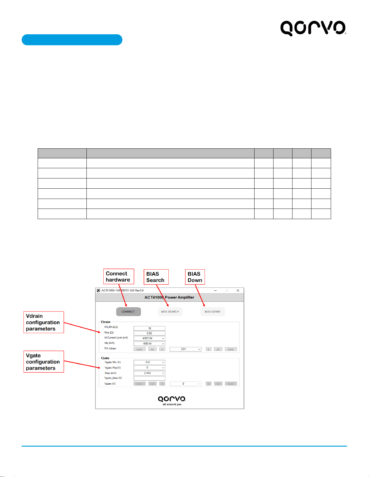
Bias Search
1. Click the BIAS SEARCH button. Note that the search routine can be stopped at any time by pressing the “STOP” button.
2. The GUI sets the ACT41000 current limit to programmed Idq Current Limit threshold and then simultaneously sweeps
the Vgate voltage while measuring the drain current. When the drain current crosses the programmed Idq threshold,
the GUI displays the optimized bias gate voltage value. If there is a setup issue and the and the optimized Vgate voltage
is not found, the GUI displays “not found”.
3. Figure 7 shows the bias search routine.
4. After the optimal bias point is found, click to either move to begin test the RF PAfunctionality or to power down the test.
To avoid damaging the RF PA, always click the “BIAS DOWN” button to power down the system.
RF Testing
1. If moving forward with RF testing, the EVK changes the ACT41000 current limit to the Id Current Limit threshold.
2. The GUI now allows the user to manually change the PAVdrain voltage and the Vgate voltage. For safety, the allowable
Vgate range is still bounded by the Vgate Min and Max settings.
3. Apply RF to the RF PA EVK.
4. To avoid damaging the RF PA, always click the “BIAS DOWN” button to power down the system.
Modifications to Test a Different RF PA
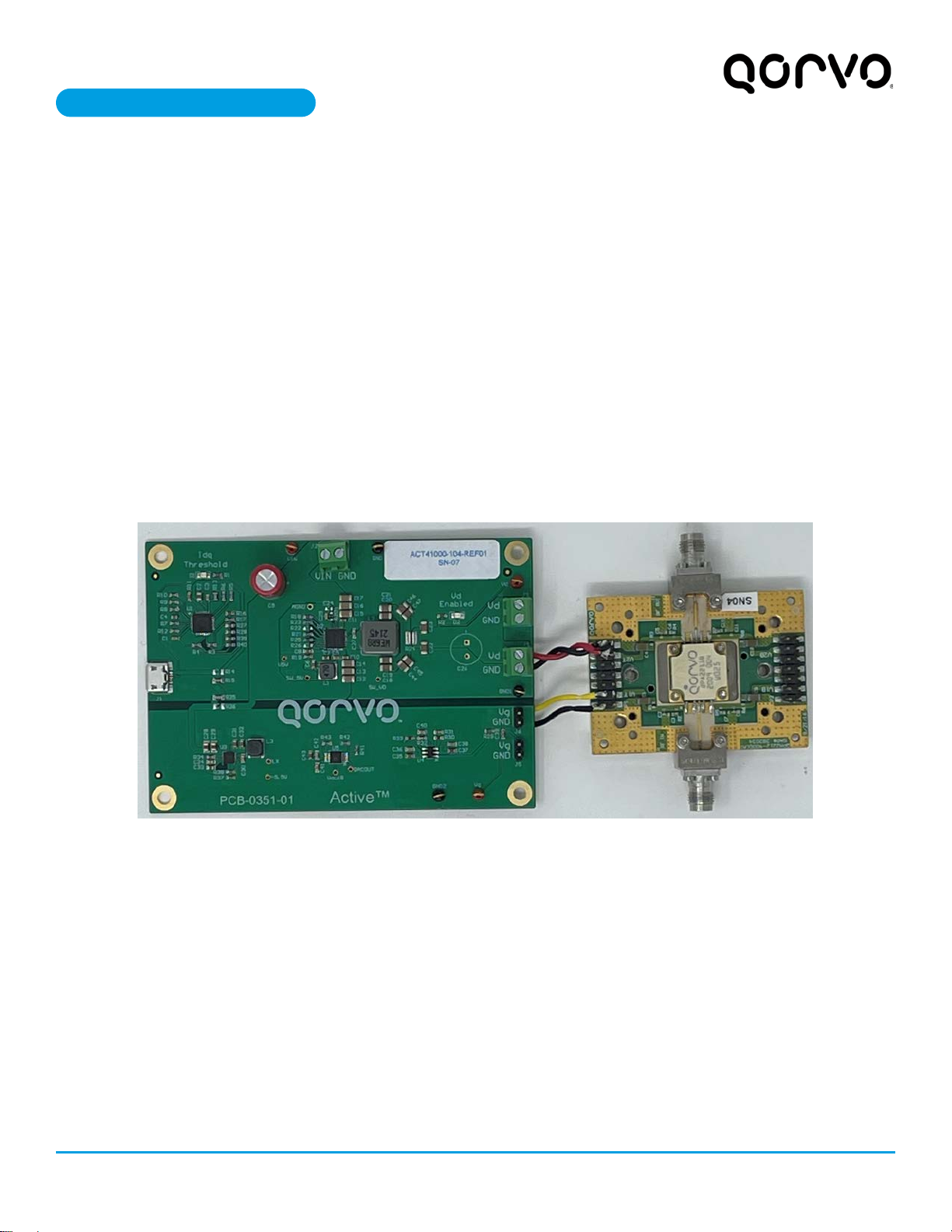
TheACT41000-104-REF01 default settings are compatible with the QPA2211. The design can be easily modified to support
any other RF PAs with drain voltages up to 24V and drain currents up to 4A. Typically, only four modifications needed to
test a different RF PA. These include the following.
PA Vdrain Voltage - Drain voltage during the search routine and the RF testing. This voltage is generated by theACT41000.
The PA drain voltage defaults to 22V but can be changed to a different voltage via the GUI. It can also be changed by
replacing the ACT41000-104 with a different version of the IC with a different default output voltage. Refer to theACT41000
datasheet for additional details and equations.
Id Current Limit – Drain current limit threshold during RF testing. This current is the same as the ACT41000EVK-104 output
current limit, which is set to 4A. The current limit is a function of the 20mΩ current sense resister (R5), the 16kΩ ILIM resistor
(R9), and the I2C ILIM Output Current Limit bits which are set to 100uA by default. The ACT41000 integrates a digital-to-
analog converter (ILIM DAC) for the purpose of generating the reference current used by the Current Limit block. Although
any of these three items can be used to change the Id Current Limit, the easiest way to change the output current limit is
with the ILIM DAC field in the GUI. Note that the RILIM and Rcs resistance values in the GUI must always match the actual
hardware values. The output current limit is easily changed by modifying any of these three parameters. Refer to the
ACT41000 datasheet for additional details and equations.
Idq Current – The RF PA Drain current threshold that corresponds to the optimal gate voltage. The Idq current setting is
achieved by changing the ACT41000 I2C ILIM current limit bits. The Idq step size is always 1/256 of the maximum Id
allowable current. If a smaller Id step size is needed, the user must reduce the maximum allowable Id current by changing
resistors on the PCB.
Vgate Min and Vgate Max – The minimum and maximum allowable voltages that can be applied to the gate. These two
voltages can only be adjusted using the GUI inputs.