UG132
1.0, 05-Dec-2019
Innovative Power
TM
ActiveSwitcher
TM
is a trademark of Qorvo.
3
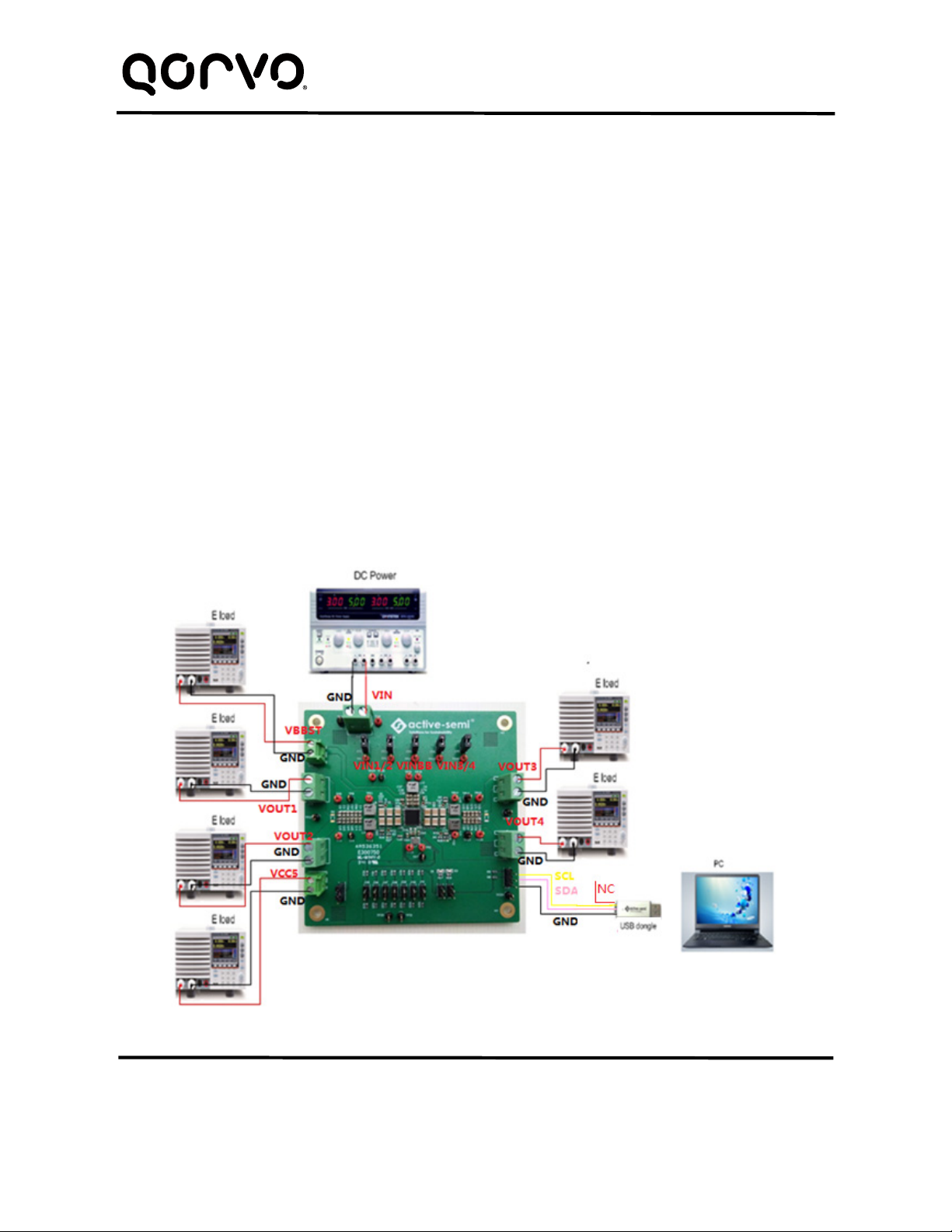
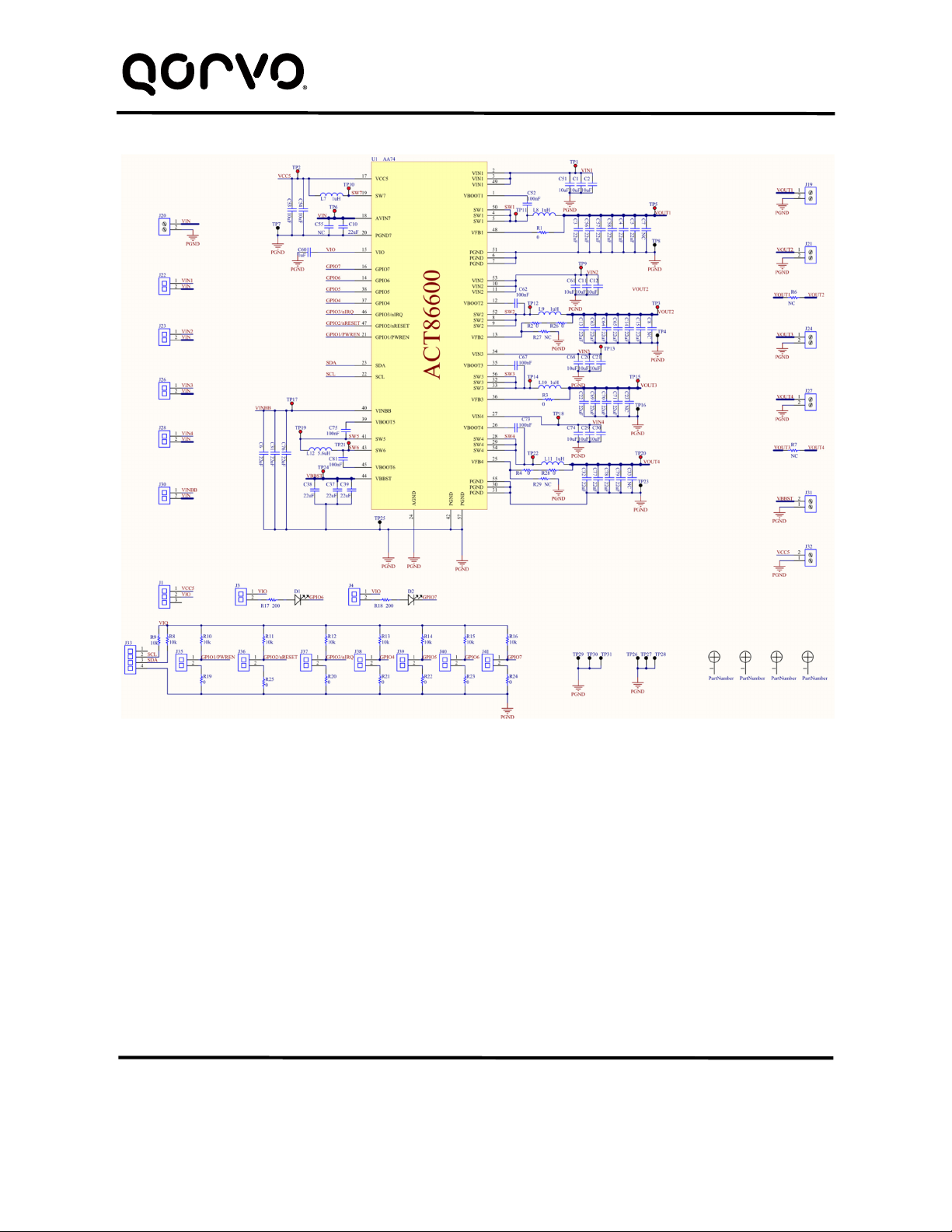
In the figure above,
VIN is input voltage to the EVK.
VIN1 is input voltage to BUCK1 and VOUT1 is the output voltage.
VIN2 is input voltage to BUCK2 and VOUT2 is the output voltage.
VIN3 is input voltage to BUCK3 and VOUT3 is the output voltage.
VIN4 is input voltage to BUCK4 and VOUT4 is the output voltage.
VINBB is input voltage to BUCK-BOOST and VBBST is the output voltage.
VCC5 is the IC’s 5.0V output
GND is the PCB’s common ground plane.
Quick Start
Hardware Setup
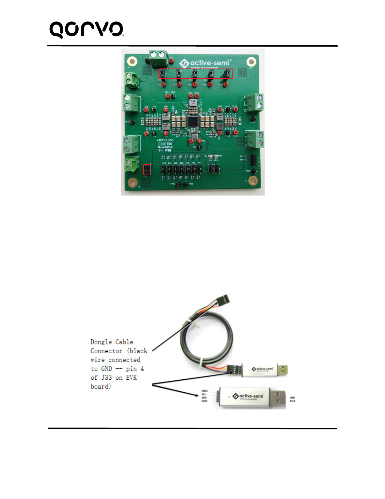
1. Decide which voltage will power VIO. Qorvo recommends powering VIO from the VCC5 output for
general evaluation. Install a shorting jumper between J1-1 and J1-2 to power VIO from VCC5. Or use
a wire to connect J1-2 to any Buck converter output.
2. Connect a lab supply between J20-1 and J20-2 to power VIN.
3. Install a shorting jumper on J22, J23, J26, J28, and J30 to power each switching converter from the
same lab supply as VIN. If a switching converter needs to be powered from a different input voltage,
remove the shorting jumper and connect that converters input to a different lab supply.
a. J22-1 powers VIN1.
b. J23-1 powers VIN2.
c. J26-1 powers VIN3.
d. J28-1 powers VIN4.
e. J30-1 powers VINBB.
4. Connect an appropriate load to each power supply output.
5. Note that the typical setup is to apply the same 12V input voltage to all inputs. VIN1/2/3/4 and VINBB
are connected to VIN by jumpers. When 12V input voltage is applied to VIN, input voltages of
VIN1/2/3/4 and VINBB will be 12V. Using different input voltage sources requires careful consideration
of startup sequencing. Each buck regulator may be connected to its own power input and it is not
mandatory to connect all regulator inputs to the same input power supply.
6. Turn on the lab supplies, and the outputs turn on and sequence up automatically.