manuals.online logo
Brands
  1. Home
  2. •
  3. Brands
  4. •
  5. QRPproject
  6. •
  7. Radio
  8. •
  9. QRPproject Blue Cool Radio User manual

QRPproject Blue Cool Radio User manual

This manual suits for next models

1

Popular Radio manuals by other brands

Grundig G6 AVIATOR owner's manual

Grundig

Grundig G6 AVIATOR owner's manual

Makita DMR114 instruction manual

Makita

Makita DMR114 instruction manual

PURE Move R3 manual

PURE

PURE Move R3 manual

Motorola CP040 Detailed service manual

Motorola

Motorola CP040 Detailed service manual

Bosch GPB18V-5C Operating/safety instructions

Bosch

Bosch GPB18V-5C Operating/safety instructions

Ocean Digital WR-230 user manual

Ocean Digital

Ocean Digital WR-230 user manual

Realistic TRC-457 owner's manual

Realistic

Realistic TRC-457 owner's manual

Uniden AX 144 owner's manual

Uniden

Uniden AX 144 owner's manual

SIGNIFY EA2173 instruction manual

SIGNIFY

SIGNIFY EA2173 instruction manual

auna multimedia 10026443 user manual

auna multimedia

auna multimedia 10026443 user manual

GME TX680 instruction manual

GME

GME TX680 instruction manual

Motorola MTM5 00 Series Basic service manual

Motorola

Motorola MTM5 00 Series Basic service manual

Tivoli Audio ONE+ owner's manual

Tivoli Audio

Tivoli Audio ONE+ owner's manual

Sirius Satellite Radio SDVK1 installation guide

Sirius Satellite Radio

Sirius Satellite Radio SDVK1 installation guide

Sirius XM RAdio EDGE user guide

Sirius XM RAdio

Sirius XM RAdio EDGE user guide

Trevi XF 100 user guide

Trevi

Trevi XF 100 user guide

EisSound KBSound iSelect user manual

EisSound

EisSound KBSound iSelect user manual

Kirisun DM588-02 user manual

Kirisun

Kirisun DM588-02 user manual

manuals.online logo
manuals.online logoBrands
  • About & Mission
  • Contact us
  • Privacy Policy
  • Terms and Conditions

Copyright 2025 Manuals.Online. All Rights Reserved.

Rev:Nobember 20. 2006
1
The blue cool Radio BCR
© QRPproject Motzener Straße 36-38 12277 Berlin http://www.QRPproject.de Telefon: +49(30) 85 96 13 23 e-mail: support@QRPproject.de
Manual written by : FIservice Peter Zenker DL2FI email:[email protected]e
Rev: November 20 2006
2
Welcome to start assembling your BCR - Blue Cool Radio. We divided the
complete kit into functional groups which can be tested individually after
assembling. Please follow the manual while assembling because each group
except the first one need the groups built before to be tested. The follow
up inside a group also is not by chance but follows logical and safety rules.
Besides this rules we tried to make it easier for you by using a graphical
coordinate system. Behind all parts you find the coordinates of the part, in
the placement plans you find the same system as a drawing. Following the
coordinates will make it easy to find the correct place for any part.
The first group to be built ist the voltage regulator section
Group 1 Voltage Regulation
BCR should be powered by a 12 Volt power supply or a package of 10 AA
NiMH cells which also give 12,0 V (Working range is 11 to 15 V). Most
stages in BCR work at stabilzed 8 V. We desided to use 8V to protect a
batterie package against low voltage which may destroy it. The choosen
regulator IC 7808 needs 9,5 V to work properly, a NiMH pack with ten AA
cells never should be used below 9,5 V.
The seperate 5V Regulator generates the supply for the central PIC
Processor which controlls the BCR.
Start at the upper left corner at coordinates A/2
Find IC 6, an 78L05 Integrated Circuit in a TO92 housing. It´s flat side
must be positioned as shown in the drawing. As allways good in RF
technique, do not solder it with
„long legs“, the lower part of the IC
should be not more the 2-3 mm
above the PCB.
[ ] IC6 8L05 TO92 A-2, solder
Tantalum Caps are polarised The PLUS side is marked either with a plus sign
(+) or a bar. Also the longer leg identifies the PLUS side. Most Tantalum
caps look like a drop.
[ ] C90 1uF 35V Tantal A-2
[ ] C91 1uF 35V Tantal A-2
Go ahead at F/5 in the lower right corner. The blocking caps often have a
right angle edge in their legs. Please take the time to rework this with a
long nose plier to make it possible to place them very flat to the PCB. If
they are placed to high above the PCB this will cause failures.
[ ] C87 100nF (104) H-4
+-
Akku 12V,intern
Bu4
12V,extern
Ladebuchse
Si1
C87D16
S2
IC5IC6 C88C89C90C91
+12V+8V+5V
Ein-Aus
100nF
1N5402
1uF1uF 780878LO5 1uF1uF
Rev:Nobember 20. 2006
3
[ ] C88 1uF 35V Tantalperle E-5
[ ] C89 1uF 35V Tantalperle E-5
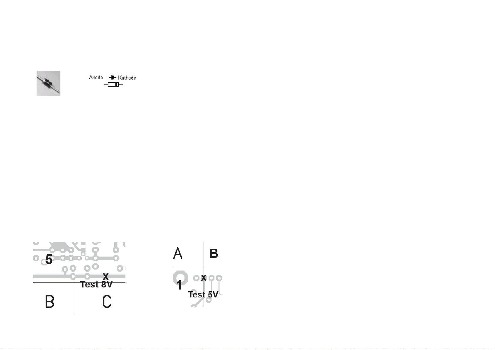
Attention: The following Diode must be placed the right way. The Kathode
of a Diode is marked by a band. If the Tyoe of the Diode is completely
coded by bands, the thickest one markes the cathode. Place the band
according to the placement plan.
[ ] D16 1N5402 G/H-5
IC5 is a voltage regulator in a TO220 Housing, which can handle about 1
Ampere at the desired Voltafe. It must be screwed directly to the PCB´s
ground plane. Because the metall plate of the IC is Ground, we need no
isolation. The printing of the IC looks to the upper side. Before installing
bend the 3 legs 90 degrees down just behind its body. Use a small
screwdriver to get a soft bent.
Screw the IC to its place before you solder it. However, it shoud lay flat on
the PCB to enable the heat to flow away.
[ ] IC5 7808 TO220 F-5
[ ] S2 Toggle Switch 2xUmupright Typ MS500 G-5
[ ] Si1 Fuse Holder G/H-5
[ ] Bu4 DCBU 2,1-PR DC Jack 2,1mm H-4/5
[ ] Si1 Put a fuse into the holder.
Now recheck all your work to find eventually solder failures. Use an
Ohmmeter to check the resistance between the switch and ground, it must
be in the range of several Kilo Ohm.
Connect a power supply. Best choise is a Laboratory supply with adjustable
current limit. Connect it to Jack BU4. Dont short the BCR Fuse with a wire,
there have been others burning their project, you better should not do so.
If you didn´t see any smoke, you now can test your work.
[ ] Test the 8 Volt stabilized line. A good access point is the solderlug at B/
5 (see picture)
[ ] Now the 5V stabilized. You find a solderlug in B1 for good access.
If both Voltages are stable at 8V and 5V +/- some percent, go ahead to
group 2, the controller section.
Rev: November 20 2006
4
Group 2 Controller Section
This section we call the digital heart of our BCR. All functions of the radio
are controlled by the Common PIC Controller. If the controller is in
function, it gives you some internal tools as an advantage: The controler
side tone enables testing the AF part, and the Controllers RF part gives us a
complete signal Generator to
test the IF section later on.
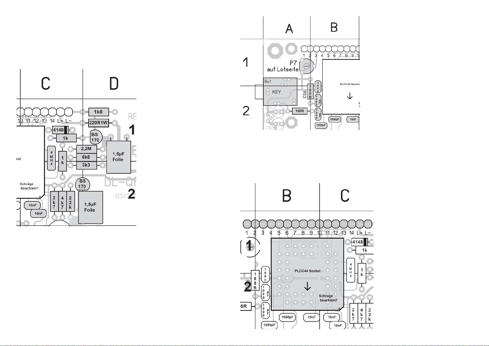
[ ] R63 not used with green
display
[ ] R54 220R 1Watt D-1
[ ] D15 1N4148 C-1
[ ] R56 1K C-1
[ ] R55 2M2 C/D-1
[ ] R62 6,8K C/D-1
[ ] R61 3,3K C/D-2
[ ] R59 1K C-1/2
[ ] R57 2,7K C-2
[ ] R58 4,7K C-2
[ ] R60 22k C-2
[ ] C86 10nF (103) C-2
[ ] C77 10nF (103) C-2
[ ] Q5 4,0MHz Resonator C-1/2
[ ] C84 1,5uF C/D-2
(This one must be installed
lying, with legs bent down by
90 degrees, otherwise you will have trouble with the display later on.
[ ] C83 1,5uF 63V Folie Also Lying D-1/2
[ ] C85 10nF (103) B-2
[ ] C80 1000pF(102) B-2
[ ] C79 1000pF (102) B-2
[ ] C78 1000pF (102) B-2
[ ] R52 100R A-2
[ ] C76 1000pF (102) B-2
[ ] C81 100nF (104) B-1/2
[ ] R53 100R A/B-1/2
[X] C82 100nF SMD 0805 Bottom
[ ] Bu1 3,5mmStereo Jack A-1/2
The following trimmer
potentiometer must be placed
at the bottom side of the PCB
[ ] P7 5K PIHER PT6 A/B-1
Now solder the socket for the PIC
and the socket for the display.
Carefully think what you are
doing, before you solder them,
especially the big PIC socket is
the hell to desolder if it is wrong.
Look at the PIC socket (PLCC
socket). One of its 4 corners
shows a 45 dgree angle. This corner must be placed into the lower left
corner as can be seen in the picture below. Place the socket on the part side
of the PCB. Again compare the 45 degree corner with the drawing. All pins
must find there way into their holes easily without forcing the socket . If it
is at its place, hold it with your fingers and control at the solder side if all
pins found their way
through the PCB. If this is
ok, firmly press the socket
against the PCB and solder
two pins at diagonal
corners. Recheck if the
socket is placed absolutely
flat on the PCB. If not,
resolder the 2 pinst while
pressing the socket down.
If it is ok, solder carefully
all remaining pins.
Use bright light and a
magnifier to controll if all
pins are soldered properly.
[ ] IC4 Socket PLCC44 B/C-
1/2
Rev:Nobember 20. 2006
5
Now the socket for the display. It helps a lot, if you use the display itself as
a justify tool. Take the display, a 16pin connector male and a 16PIN
connector female plus 4 of the 12mm spacers and the small 2mm Screws.
Do not solder yet.
Place the 16pin female connector into the mainboard.
Plug the 16pin male connector into the female connector
Place the display on the upper pins of the male connector. The ends of the
pins look through the holes of the display. Now mount the 4 spacers at all 4
corners of the display between main board and display. Fasten all 4 screws
while holding the display. 16pin connectors must be as exact as possible in
a 90 degree angle on to the mainboard. If this is ok, solder the pins at the
bottom of the mother board and the display board. The ends of the
connector Pins will just flush with the PCB but this is ok because the boards
are throughplated. Start with the outer pins, check again the right angle. If
ok, solder the remaining pins.
[ ] Disp1 16 PIN male, straight A/B/C-1
[ ] Disp2 16 PIN female straight A/B/C-1
[ ] DiSP3 LCD-Display DEM 16216 SYH-LY
[ ] Remove the Display and put the Display, screws and spacers to a safe
place.
Now the C-Mos Transistors. Remember, they are extremly ESD sensitive. Use
ESD tools or decharge yourself by touching a metal ground plate.
(Drawing = first picture section 2)
[ ] T16 BS170 C/D-2
[ ] T17 BS170 C/D-1 There ar e only a few parts left: :
[ ] L10 33mH radial Choke C-2/3
[ ] P8 10K Potentiometer SMC-10-V
B/C-3
[ ] DG1 Shaft encoder ALPS
A/B-3
To complete the controller section, you
now need the DDS Modul. If you got it ready built and tested from
QRPproject, go ahead to the next page where the connectors are installed.
Otherwise assemble the DDS Module now.
Assembling the DDS Modul:
If you have own expierience in soldering SMT parts, you may start
immediate. If not, I recommend to read something about SMT soldering or
to ask an OM with some expierience.
Start with IC1. Adjust it carefully above the Pads, the Dot mus show to the
Callsign upper left corner. Solder to edge pins, controll the pposition again
and solder the remaining pins.
[ ] IC 1 AD9834
Now the other parts from left to rights:
[ ] C1 100nF 0805 [ ] R1 150R 0805
[ ] C2 100nF 0805 [ ] R3 10R 0805
[ ] R2 10R 0805 [ ] C4 10uF Tantal Gr. B
[ ] C3 10uF Tantal Gr. B [ ] C6 100nF 0805
[ ] C5 100nF 0805 [ ] C9 10nF 0805
[ ] C10 100nF 0805 [ ] R4 6k8 0805
[ ] C7 100nF 0805 [ ] C8 10nF 0805
[ ] R5 220R 0805 [ ] R6 220R 0805
[ ] C11 39pF 0805 [ ] L1 1,8uF 0805
[ ] C12 5,6pF 0805 [ ] C13 68pF 0805
[ ] L2 1uH 0805 [ ] C14 5p6 0805
[ ] C15 39pF 0805 [ ] C16 10nF 0805
Rev: November 20 2006
6
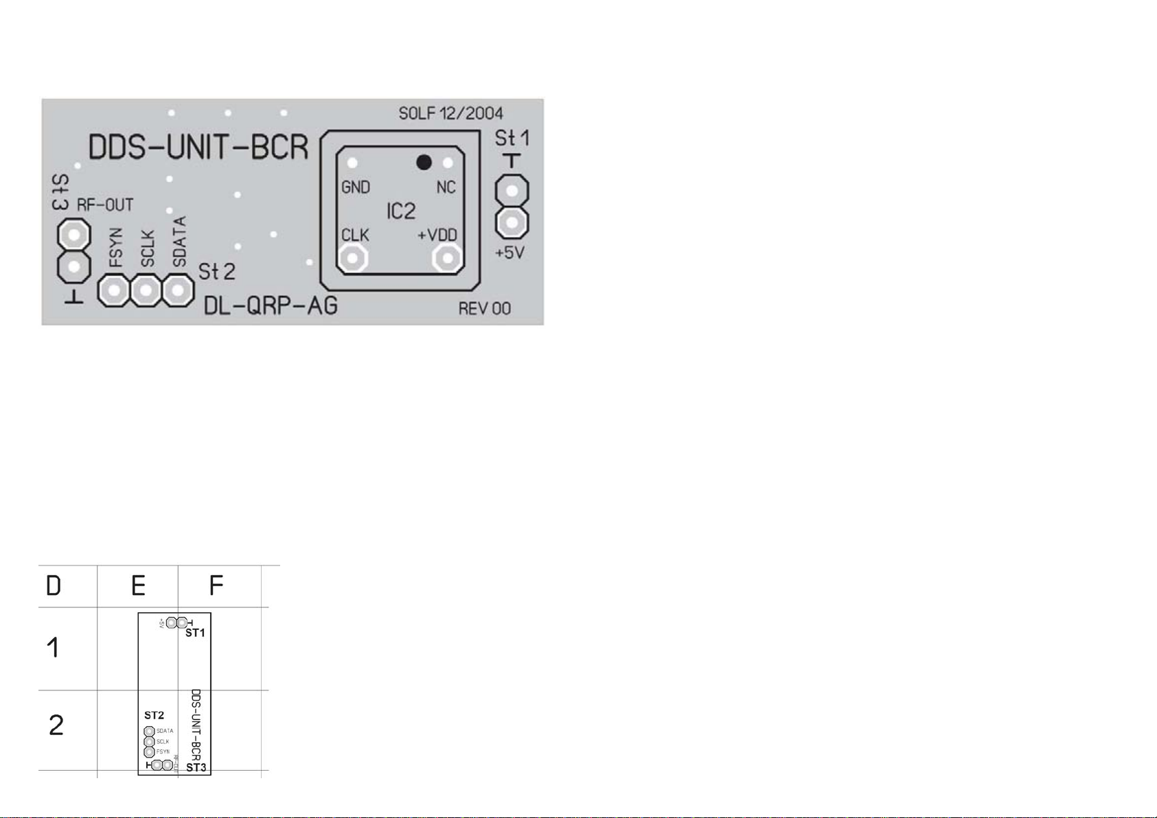
Now turn around the PCB. Here you will install the Clock Oscillator and the
3 connectors.
Solder first the integrated Clock. Take care to place the sharp edge to the
upper right corner as shopwn in the picture.
[ ] Clock oscillator
Now mount the 2x2pin and 1x3 pin male connectors. They are placed at the
side where the clock is and soldered at the side where the DDS is. Adjust
them to a 90 degree angle before soldering.
[ ] ST1 connector 2 Pin male
[ ] ST2 connector 3 Pin male
[ ] ST3 connector 2 Pin male
Starting her,e same prodedure for
both, ready made and self soldered
DDS Modules:
Place the female connectors into their
holes, place the modules into the
connectors, adjust the modul on the
connectors and solder.
[ ] ST1 2 PIN female, 90degrees angle
on Mainboard, solder from solder side.
[ ] ST2 3 PIN same
[ ] ST3 2 PIN same
Now place the PIC processor itself into the socket. Find at first the 45
degree side of the PIC. This side must look to the inner part of the PCB.
Dont force too much power while pressing the PIC into the socket, it must
find its place very smooth.
[ ] IC4 PIC16F877 PLCC + B/C-1/2
[ ] Reinstall the Display
[ ] Install the DDS Module
Check all your work with a magnifier for shorts and unsoldered Pins. If this
is ok, apply 12 Volt and start testing of section 2.
After power on, adjust Contrast Pot P7 (on solder side of the PCB) to make
the signs in the display readable. If so, swith power off an on again.
The display should show it´s initial sequence for a short time: Blue cool
Radio and the Firmware revision e.g. 1.14. After the initial frequency it
should show VFO A and B both at 7030 kHz.
At St3 RF- 0ut you will find the RF output of the DDS. Though the
controller is in receive mode, the generated RF is calculated: Display
frequency plus or minus RF depending on the band. You may control it with
a receiver or a counter if you want so. Because most of you will play with
the controller menue, we go on with the description of the Firmware now.
How to use the DDS_BCR
Press the Shaft encoder short: Change Rate sequential 10Hz, 50 Hz, 1kHz
If you are in „Radio“ mode, 100kHz rate is added. Change of rate is
signalized by a short beep (later on, if the AF is installed) Rate is displayed
by decimal point /resolution of the shown frequency.
Press shaft encoder long (> 1s) The display will switch to MENUE.
By turning the shaft encoder, you scroll through the menue
Menue:
0 break Leave the menue without changing anything
1 VFO A/B Switch between VFO A/B
2 Band 0 80m (only available with built in 80m Option) Switch to 80m by
pressing the shaft encoder. Actual frequency of actual band will be
Rev:Nobember 20. 2006
7
stored.
2 Band 1 40m Switch to 40m by pressing the Shaft encoder. Actual fre-
quency of actual band will be stored.
3 Band 2 30m Switch to 30m by pressing the Shaft encoder. Actual fre-
quency of actual band will be stored.
4 Band 3 20m Switch to 20m by pressing the Shaft encoder. Actual fre-
quency of actual band will be stored.
5 Band 4 17m Switch to 17m by pressing the Shaft encoder. Actual fre-
quency of actual band will be stored.
6 Band 5 Radio Switch to Radio (Braoadcast) by pressing the Shaft enco-
der. Actual frequency of actual band will be stored. In Radio Mode TX is
inhibited and 100kHz steps is added.
7 light on/off Backlight on / off. If you see ON in the display, pressing the
shaft encoder will switch to ON. If you see OFF in the display, pressing
the shaft encoder will switch to OFF
8 light auto Backlight automatic. If ON, any touch of the Dial will switch
the backlight on. Backlight switches to off automatically after 2 s inacti-
vity
9 SETUP start of the SETUP Menu
10 keyer Internal keyer electrinic ON /OFF
11 memory read Reads memory. The PIC stores up to 20 Frequencies (num-
ber 01 to 20, shown in the upper left corner of the display. Each Memory
place stores Bandnumber plus Frequency for VFOA and VFOB. With the
shaft encoder you can choose the memory number, the content of the
memory is shown in the display. Cancel stops the operation. There are
two ways to choose the memory contents:
1. Shortly pressing the shaft encoder (only 1 beep) overtakes the stored
frequencies into VFO A/B and switches to the band.
2. Pressing the Shaft encoder long overtakes the frequencies into the VFO
and starts the SCAN function. During Scan the Controller stops for any
recognized signal for a short time. Touching the CW key or the Shaftenco-
der stops scanning at this frequency. Scan allways goes from A to B so
Frequency A allways must be lower then frequency B. ATTENTION: Use
only logical values, otherwise the controller will „hang up“ . If you run in
such a situation the only way to get out is the „Set Default“ function.
12 memory store Write top Memoryr. Choose the Memory like in Menue 12.
Store the actual VFO and Band information by pressing the Shaft encoder.
Any content in the memory will be overwritten.
13 tune. Switches the transmitter to TUNE. During TUNE power and SWR
are displayed.
14 split 1k DDS switches VFO A to receive only and VFO B to transmit only.
TX VFO starts exactly 1 kHz above the RX frequency. The Shaft encoder
now changes only the TX frequency, RX stays stable
15 split 2k DDS switches VFO A to receive only and VFO B to transmitt
only. TX VFO starts exactly 2 kHz above the RX frequency. The Shaft
encoder now changes only the TX frequency, RX stays stable
16 rit Rit on /off. If ON, Row 1 in the display shows RX frequency, row 2
shows TX frequency, original frequency of row 1 was copied to row 2
while switching. Shaft encoder actuates only the RX, TX stays stable.
Paddle in combination with the Shaftencoder:
SPOT: Press shaft encoder end Dot Paddle at the same time. Sidetone is
activated, rate switched to 10 Hz. With the shaft encoder you can adjust
a received CW signal exactlxy to your sidetone which makes your BCR
transceive.
TUNE Press shaftencoder and Dash paddle at the same time. Controller
switches to „TUNE“ mode
SETUP
Go to Menue, choose Setup.
0 Setup break Ends setup Menue, causes hard reset of the controller.
1 DDS-Takt Here you can adjust the clock oscillator. Valu is shown as Hex
Number. ATTENTION: if you store a complete wrong value here, the DDS
will not work any longer. Pressing the Shaft encoder will cause cursor to
go from left to right. Left side are the coarse bits and right side the fine
bits. Right of the lowest bit you will find left, save, cancel. At start the
DDS generates 6075,000 Khz +/. some Hz depending on the Clock fre-
quency. By variing the Hex Number, you can change the generated Fre-
quency until it is exactly 6075,000 kHz. You do this by comparing it with
a good counter or by zerobeating „Deutsche Welle“ at 6075kHz in a
shortwave Radio ( establish a link between DDS Modul and a radio. Tune
the radio to Deutsche Welle. You will hear the DDS as a tone if it is not
exactly at the same frequency. Now tune the DDS until the tone is zero.
If you got the DDS to the correct frequency, use SAVE at the right side to
Rev: November 20 2006
8
store the calibration factor into memory. From now the DDS will generate
very exactly th echoosen frequency
2 ZF (Hz) Here you can adjust the exact IF. The DDS at starting point
generates the estimated IF of BCR which is a little bit lower the the Xtal
frequency (that´s typical for ladder filters). The frequency is shown in the
display in decimal values. The complete procedure is described in the IF
section of the manual.
3 S-Meter Eich S-Meter calibration Menue
1. : No Antenna, Antenna jack open or Dummyload installed (S0). Hex-
value is shown. Press shaft encoder, menue will jump to point 2
2: Apply 50uV ato the Antenna jack, measured Hexvalue is shown. Press
Shaftencoder and leave th eMenbu by SAVE. The Pic will calculate the S-
Meter curve now and store it into memory.
4 pitch Frequency of the sidetone can be choosen by the CW speed poty.
Last stored value shown in the display. The choosen tone frequency must
be aligned with the BFO Frequency during IF adjustment to be transceive.
6 set default This is the „SOS“ point, if all fails. Set default fills all memo-
ries with logicak values. All adjustments will be lost.
Coose „0 Setup break“ to leave the setup Menue
Rev:Nobember 20. 2006
9
Group 3 AF Section
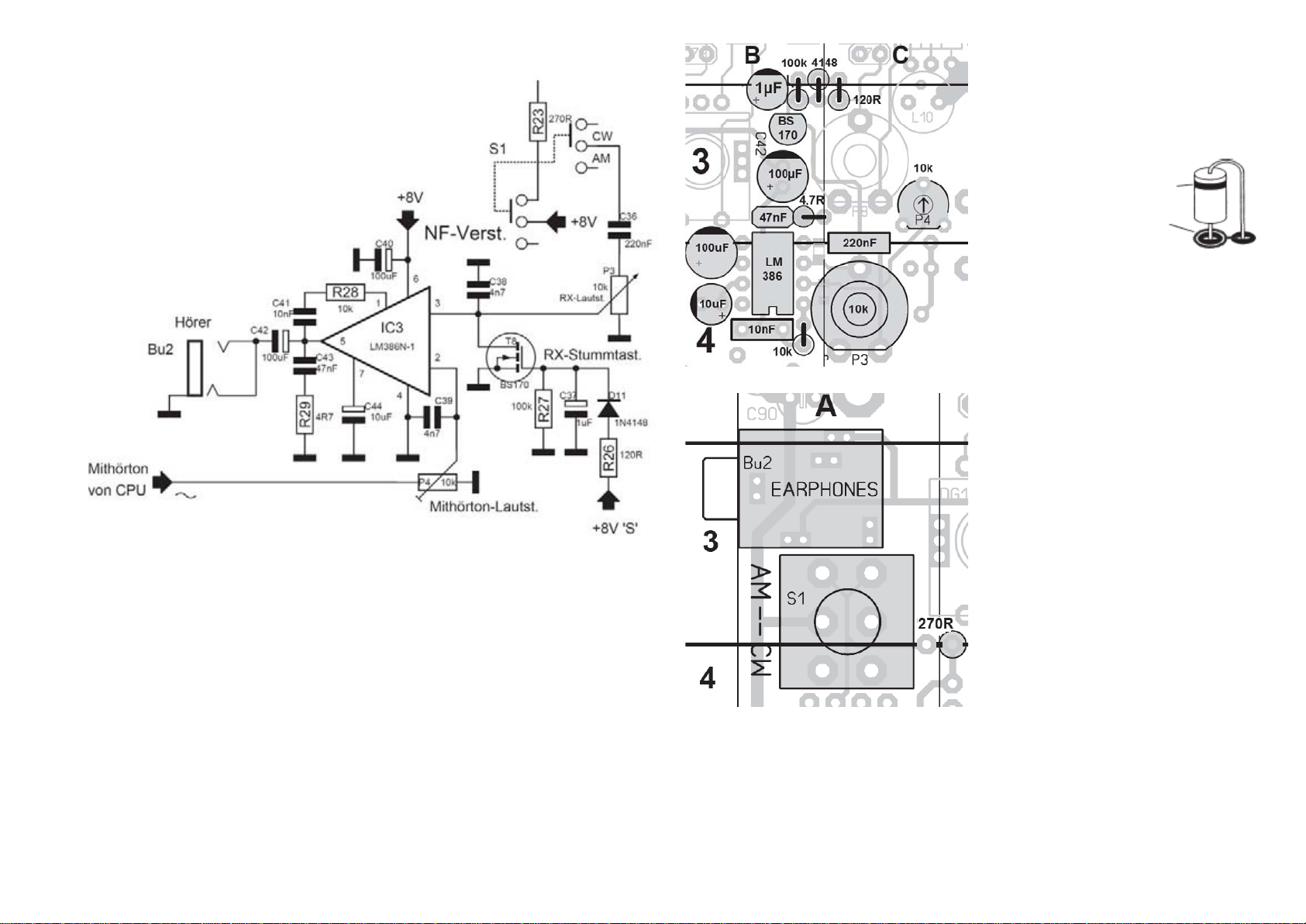
There are only a few parts in Section 3. It represents the AF Amplifier for
both, the received Signals and the TX-sidetone. The AF Amplifier is designed
to drive standard low impedance stereo headphones. Loudness of the
sidetone can be adjusted independent from receiver loudness by trimmpot
P4.
Start with installation of IC3 because it´s easier to be installed if space
around is free of other parts.
[ ] IC3 LM386 B-3/4
[ ] C4110nF Foile spaced 5mm B-4
[ ] R28 10K upright B-4
[ ] C44 10uF 35V rad. B-4
[ ] C40 100uF 16V rad. B-3/4
[ ] C43 47nF (473) B-3
[ ] C36 220nF Foil spaced 5mm
C-3/4
[ ] R29 4,7R upright B-3
[ ] C42 100uF rad. B-3
[ ] R26 120R upright
C-3
Install fullowing diode
also upright. There is a
convention to place
the cathode (banded
side) to th eupper end.
The body is placed inside the printed
circle in the placement plan.
[ ] D11 1N4148 B/C-2/3
[ ] R27 100K upright B-3
[ ] C37 1uF rad B-2/3
[ X] C38 4,7nF SMD 0805 bottom of
PCB
[ X] C39 4,7nF SMD 0805 bottom of
PCB
[ ] R23 270R upright A/B-3/4
[ ] Bu2 3,5mm Stereo Jack A-2/3
[ ] P3 10K Potentiometer SMC-10-V
B/C-4
[ ] P4 10K PT6 Trimmpoti C-3
Remember ESD safety rules if you
install th etransistor!!
[ ] T8 BS170 B-3
[ ] S1 Toggle Switch 2xUm A-3/4
If you again have checked your Work with a magnifier to find possible shorts
and forgotten solder points, you need a headphone and a key to test this
group. If you use a paddle, it must have a 3,5mm Stereo plug with
following connections: Paddle: Tip = Dot, Ring = Dash, Back = Ground.
Handkey (Pumpkey) : Tip and Ground,don´t connect the ring. Switch power
Rev: November 20 2006
10
on and press the key or the dot paddle. You should here the sidetone.
Adjust the level by P4. Go ahead with section 4.
Baugruppe 4 ZF Verstärker / BFO
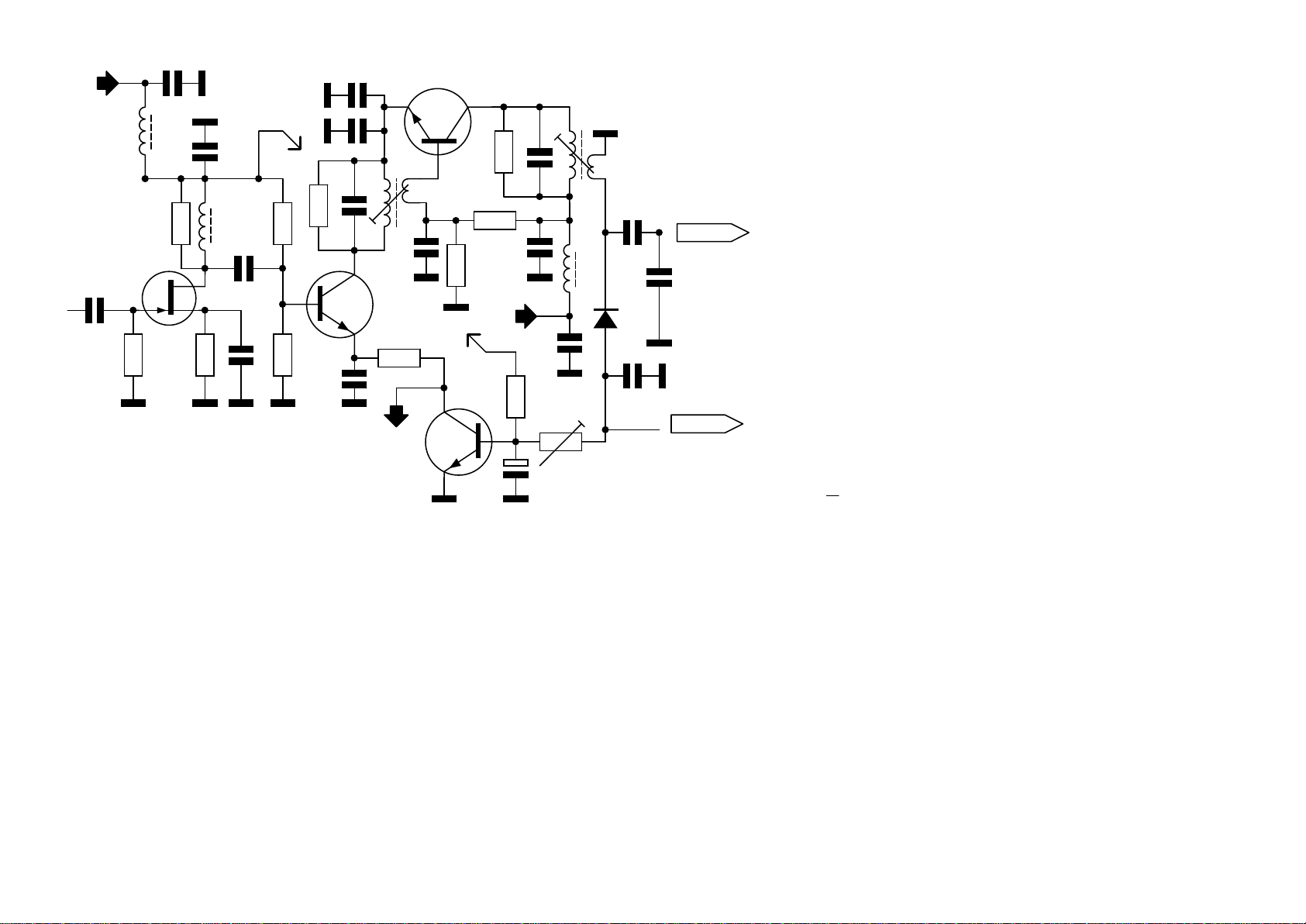
The FET amplifier T3 together with the transformer Dr4/C16 acts as coupler
to couple the impedance of the Ladderfilter to the selectiv amplifier T4/T5.
As far as we know, the design of the following cascaded IF Amplifier by
Peter, DK1HE is absolutely unique and new. You will enjoy it´s features after
your BCR is ready built.
Transistors T4/T5 are in terms of DC serial cascaded and use half of the
Voltage (4V) each. The commen collector current is adjusted by R14 to
about 3,5mA which is significant low compared
to two seperate driven singel Amplifier stages.
By T6 easily the current through the complete
chain can be varied and by this, the Gain factor
of T4/T5 that means the gain of the IF amplifier
can be regulated. In Terms of RF the amplifier
works conventional. C20/C21 decouple both
stages. T4 does not work with the low input
impedance T5 but its working resitance is the
resonate circuit L4/C9 which gives us much
higher gain per stage.
Output of T5 is working with the resonate
circuit L5/C24. By damping resistors R13/R18
the total unregulated gain is adjusted to about
70 dB.
The IF signal is inductiv coupled by L5 to the
following product detector T7 and diode D10.
D10 has to do 2 jobs: 1. it is used as AM
Detector if BCR is used in AM with BFO switched
off and 2. it generates the AGC Voltage directle
from the IF without an extra amplifier. The AGC
curve can be adjusted by P5.
D10 generates a negative voltage which is
proportional to to the IF Voltage. The neagtiv
voltage reduces the base current of T6 in
conjunction with the fieldstrength of the
received signal, so the total collector currend
and total gain decrease. 0dBm (220mV) at the antenna can be kept by the
AGC without any distortions. Because D10 is used with a negativ Voltage,
eben very small signals can start the AGC. By its negativ temperatur
coefficient D10 compensates the tempereratur sensible base-emitter
junction of T6. The AGC works stable over a wide temperature range.
CW and SSB denodulation is done by the MOS tetrode T7. To keep the
number of parts low, it is designed as a self oscillating mixer. The BFO
Quatz is oscillating with an offset of 500-900 Hz. Behind the Lowpas R24/
C35 there is an AF signal, which can be handled by the AF amplifier.
ZF-Vorverst.
ZF-Verstärker
ZF-Verst.-Regelung
+8V
AGC-Spannung
0,2-1V
+8V
T3
T4
T5
T6
D10
P5
C11
C14
C15
C16
C17
C18
R8
R9 R10
R11R12
R13
R14
R15
R16
R17
R18
zu CPU
A
A
C19
C20
C21
C22 C23
C24
C25
C26
C27
C28
L4
L5
1
2
3
4
1
23
4
Dr3- 100uH
Dr4- 33uH
Dr5 - 100uH
0,47uF
50k
1N4148
47nF
47nF
150p
18Wdg 6Wdg
6,8nF
470k
270R
BC550
BF199
BF199
47nF
47nF
8k2
12k
47nF
entfällt
150p
3k3
12k
33pF
47nF 47nF
2Wdg
18Wdg
3k9
270R
1k
150pF
47nF
47nF
2k2
BF244A
Baugruppe ZF-Verstärker / BFO
C92
22p
BFO
AM Signal