Realtek RTL8762C User manual

RealtekConfidential
RTL8762C Evaluation Board User Manual
V1.0
2018/09/17

RealtekConfidential
RTL8762C Evaluation Board User Manual
2
Copyright 2018 Realtek Semiconductor Corporation.
All Rights Reserved.
Revision History
Date
Version
Amendment
Author
2018/07/07
V1.0
First Draft
Jason_Xue
2018/09/19
V2.0
Second Draft
Jason_Xue

RealtekConfidential
RTL8762C Evaluation Board User Manual
3
Copyright 2018 Realtek Semiconductor Corporation.
All Rights Reserved.
Contents
Revision History................................................................................................................................................ 2
Contents of Tables............................................................................................................................................. 4
Contents of Figures............................................................................................................................................ 5
1.RTL8762C Evaluation Board Introduction.................................................................................................... 6
1.1 RTL8762C EVB introduction ................................................................................................................. 6
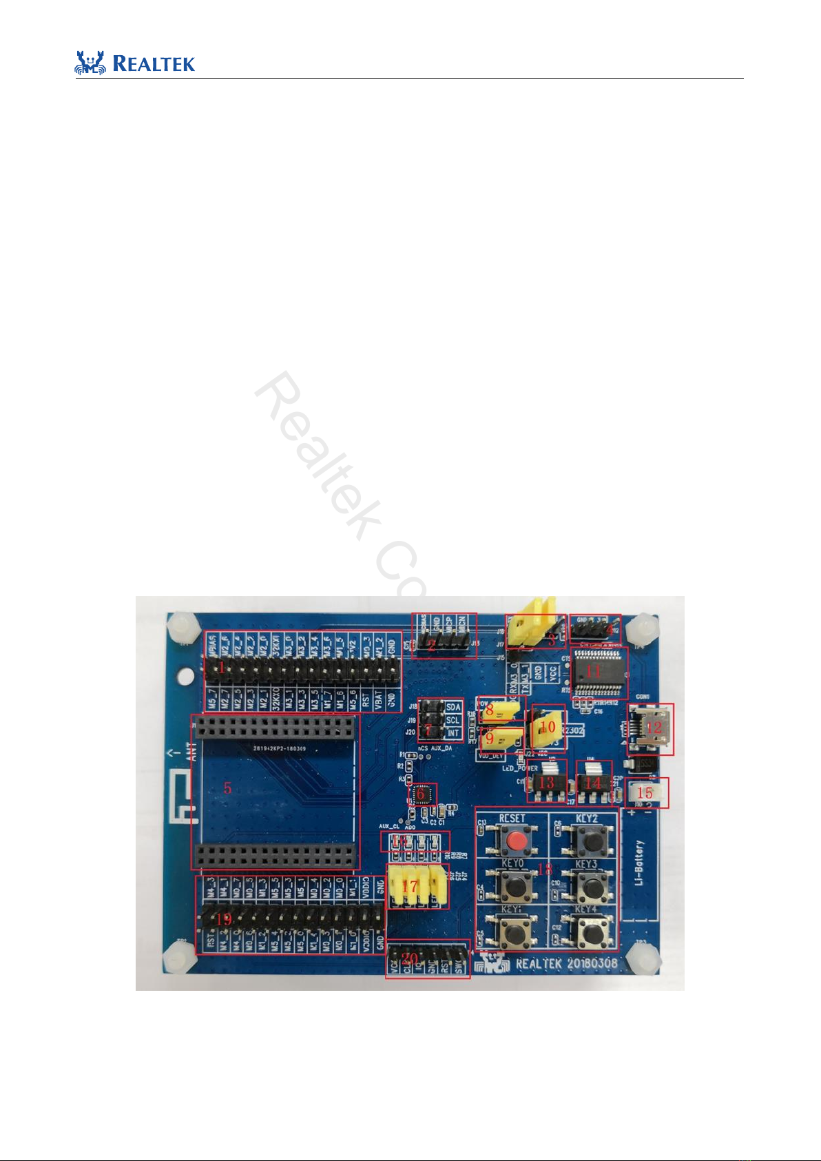
1.2 Evaluation Board Interface...................................................................................................................... 6
1.2.1 Interface Description ........................................................................................................................ 6
1.2.2 Main Chip (Module)......................................................................................................................... 7
1.2.3 Power supply.................................................................................................................................... 8
1.2.4 IO Port .............................................................................................................................................. 9
1.2.5 Interface............................................................................................................................................ 9
1.2.6 Others ............................................................................................................................................. 10
1.2.7 Pin Allocation on Motherboard of Evaluation Board..................................................................... 11
2.Development Board Operation Instructions................................................................................................. 13
2.1 Acquiring Log with Onboard USB to UART Converter....................................................................... 13
2.2 Current test ............................................................................................................................................ 13
2.3 6-axis Motion Sensor............................................................................................................................. 14

RealtekConfidential
RTL8762C Evaluation Board User Manual
4
Copyright 2018 Realtek Semiconductor Corporation.
All Rights Reserved.
Contents of Tables
Table 1.1 IO Pin Allocation on Motherboard...........................................................................................................11

RealtekConfidential
RTL8762C Evaluation Board User Manual
5
Copyright 2018 Realtek Semiconductor Corporation.
All Rights Reserved.
Contents of Figures
Figure 1-1 EVB Interface Block Diagram.............................................................................................................. 6
Figure 1-2 EVB Interface Distribution................................................................................................................... 7
Figure 1-3 Daughter Board..................................................................................................................................... 7
Figure 1-4 Power jumper........................................................................................................................................ 8
Figure 1-5 Connection of HCI UART Jumper........................................................................................................ 9
Figure 1-6 Connection of LOG............................................................................................................................... 9
Figure 1-7 G-sensor I2C connection..................................................................................................................... 10
Figure 1-8 Schematic of LED circuit.................................................................................................................... 10
Figure 1-9 Schematic of Keys ...............................................................................................................................11
Figure 2-1 LOG out connection............................................................................................................................ 13
Figure 2-2 Schematic of Power jumpers on EVB................................................................................................. 13

RealtekConfidential
RTL8762C Evaluation Board User Manual
6
Copyright 2018 Realtek Semiconductor Corporation.
All Rights Reserved.
1.RTL8762C Evaluation Board Introduction
1.1 RTL8762C EVB introduction
This document introduces usage of 8762C Bluetooth® Evaluation Board (EVB) Hardware. 8762C EVB provides
hardware environment for customer to develop their own application, which includes:
1. Voltage converter.
2. 6-axis motion sensor.
3. 4 LEDs and 6 keys.
4. Button battery and Li-ion battery holder.
5. USB to UART converter (FT232RL).
1.2 Evaluation Board Interface
1.2.1 Interface Description
Distribution of EVB block and interface is shown in Figure 1-1 and Figure 1-2.
Figure 1-1 EVB Interface Block Diagram

RealtekConfidential
RTL8762C Evaluation Board User Manual
7
Copyright 2018 Realtek Semiconductor Corporation.
All Rights Reserved.
916.3408
P0_2
GND
M4_1
P3_3
P3_5
P0_0
P0_4
P0_6
P4_0
P4_3
M5_4
RST
M4_2
M4_0
M0_6
M1_2
M5_2
M5_0
M1_4
M0_3
P4_3M0_1
P0_4
VDDIO
GND
M1_0
VDDIO
GND
32KXI_GPIO
MICBIAS
M2_6
M2_4
M2_2
M2_0
M3_0
M3_2
M3_4
M3_6
32KXO_GPIO
M5_7
M2_7
M2_5
M2_3
M2_1
M3_1
M3_3
M3_5
M3_7
M1_5
1V2
M0_3
M1_2
M1_6
M5_6
RST
VBAT
GNDGND
SWD
Interface
VCC
CLK
IO
GND
RST
SWO
MICBIAS
GND
MIC_P
MIC_N
LOG
UART
Interface
FT232_RX
FT232_TX
TX
RX
GND
VCC
GND
GND
GND
KEY1(M4_1)
KEY0(M4_0)
RST
KEY4(M2_5)
KEY3(2_3)
KEY2(2_4)
LED3(M1_4)
LED2(M1_3)
LED1(M0_2)
LED0(M0_1)
LED3_JP
LED2_JP
LED1_JP
LED0_JP
VDEV_JP PowTest_JP
LDO_3V3 P4_5VDD_OUT P4_5
LDO_2V5
P4_5VCR2302
UART
Interface
LED1_JP
LED0_JP
Power
LED/Key
IO
Interface
Figure 1-2 EVB Interface Distribution
1.2.2 Main Chip (Module)
Mark 5: Connection socket used to connect daughter board with mother board. Make sure that the orientation of
PCB antenna on daughter board is the same as the silkscreen mark of antenna on mother board. Daughter board is
shown in Figure 1-3.
Figure 1-3 Daughter Board

RealtekConfidential
RTL8762C Evaluation Board User Manual
8
Copyright 2018 Realtek Semiconductor Corporation.
All Rights Reserved.
1.2.3 Power supply
1) Mark 10: Power supply selection module of motherboard, shown in Figure 1-4.
Figure 1-4 Power jumper
a) 3V3:Powered by USB power source on evaluation board, IC voltage 3.3V.
b) VCR2302: Powered by a CR2302 battery (on the rear)
c) 2V5:Powered by USB on evaluation board, IC voltage is 2.5V, generally used while burning eFUSE.
2) Mark 21: CR2032 battery holder (at the bottom side of PCB)
3) Mark 15: Li-ion battery holder: evaluation board can be powered by Lithium-ion battery.
Note: If EVB is powered by Li-ion battery, jumper cannot be put on mark 10.
4) Mark 13/14: AMS1117 3.3V output and AMS1117 2.5V output LDP chip that provide 5V to 3.3V and 5V to
2.5V voltage conversion circuit when EVB is powered by Li-ion battery.
5) Mark 9: Power G-sensor and SWD VCC. This jumper must be connected during normal operation.
6) Mark 8: Jumper for RTL8762C overall power consumption test. Remove J23 and cascade with an ammeter
when performing overall power consumption test.
Note:
a) J23 must be shorted during normal operation.
b) When performing current measurement, LOG printed must be disabled. UART should be left not
connected and disconnect SWD with debugger to avoid affecting measurement.
c) Under some special circumstance that current measurement at 3V needs to be performed, replace
onboard power supply with external 3V DC power supply.
7) Mark 12: Micro USB 5V power supply. It can be connected to either external 5V power supply or USB port
of PC.

RealtekConfidential
RTL8762C Evaluation Board User Manual
9
Copyright 2018 Realtek Semiconductor Corporation.
All Rights Reserved.
8) Mark 4: GND jumper.
1.2.4 IO Port
1) Mark 1: 2 × 15 IO Jumper
2) Mark 19: 2 × 14 IO Jumper
1.2.5 Interface
1) Mark 2: MIC Test Jumper for external MIC
2) Mark 3: UART /LOG Test Jumper.
a) Connection of Jumper for HCI UART Test is shown in figure 1-5:
Figure 1-5 Connection of HCI UART Jumper
b) Connection of Jumper for Log Test:
Figure 1-6 Connection of LOG
3) Mark 6: G-sensor, which is a 6-axis motion sensor, is powered by VDD_DEV. Thus, J6 need be connected
when G-sensor is required.
4) Mark 7: I2C interface of 6-axis motion sensor. Connection of Jumper J18, J19 and J20 is shown in figure

RealtekConfidential
RTL8762C Evaluation Board User Manual
10
Copyright 2018 Realtek Semiconductor Corporation.
All Rights Reserved.
1-7.
If I2C interface is applied, J18 and J19 should be shorted with jumper. That is to say, connect I2C signal line
to M3_2 and M3-3. INT single line can be connected to M2_2 via J20, and can be left not connected if INT
function is not configured.
If SPI interface is applied, R1 need be removed. Connect test point AD0 and nCS to specified IO port with
SDO and nCS jump wire respectively, and then short J18 and J19 with jumper.
Figure 1-7 G-sensor I2C connection
5) Mark 12: Micro USB interface. It can be used as UART communication port when connected to PC.
6) Mark 20: SWD interface used for SWD debug.
1.2.6 Others
1) Mark 16: 4 independent LED used for development of customized application. Confirm that corresponding
jumpers (J24 to J27) are connected properly before develop. Schematic is shown in figure 1-8.
Figure 1-8 Schematic of LED circuit
2) Mark 17: 4 LED jumpers. When testing power consumption, LED may be lighted up and affect result of test.
Under such circumstance, LED Jumpers should be removed. Default LED configuration is provided in table
1-1. If customers would like to use IOs that not listed in table 1-1 to control LEDs, LEDs can be connected to

RealtekConfidential
RTL8762C Evaluation Board User Manual
11
Copyright 2018 Realtek Semiconductor Corporation.
All Rights Reserved.
specified IO port with jump wire.
3) Mark 18: RESET key and 5 independent keys, as shown in Figure 1-9.
Note: Debouncing capacitors and internal pull-up resistor make up a filter circuit to reduce ripples when
buttons are pressed. However, it can also affect the result of keyboard array scan. Capacitors are not
mounted on board by default. User can solder 0.1uF capacitor on pads when necessary.
Figure 1-9 Schematic of Keys
4) Mark 11: FT232 chip.
1.2.7 Pin Allocation on Motherboard of Evaluation Board
When edges of daughter board are flush with the white lines and PCB antenna on daughter board is aligned with
silkscreen mark on motherboard, the pins on daughter board are properly inserted; otherwise it is necessary to be
cautious about improper connection.
Pin allocation of motherboard is listed as follows:
Table 1.1 IO Pin Allocation on Motherboard & Daughterboard
RTL8762CJ
RTL8752CJ
RTL8762CJF
RTL8752CJF
RTL8762CK
RTL8762CKF
EVB
FunctIOn
EVB socket
P0_0
P0_0
P0_0
P0_0
M0_0
P0_1
P0_1
P0_1
P0_1
LED0
M0_1
P0_2
P0_2
P0_2
P0_2
LED1
M0_2
P0_3
P0_3
P0_3
P0_3
LOG
M0_3
P0_4
P0_4
P0_4
P0_4
M0_4
P0_5
P0_5
P0_5
P0_5
M0_5
P0_6
P0_6
P0_6
P0_6
M0_6
P0_7
P0_7
P0_7
P0_7
M0_7

RealtekConfidential
RTL8762C Evaluation Board User Manual
12
Copyright 2018 Realtek Semiconductor Corporation.
All Rights Reserved.
P1_0
P1_0
P1_0
P1_0
SWDIO
M1_0
P1_1
P1_1
P1_1
P1_1
SWDCLK
M1_1
P1_2
P1_2
P1_2
P1_2
M1_2
P1_3
P1_3
P1_3
LED2
M1_3
P1_4
P1_4
P1_4
LED3
M1_4
P1_5
P1_5
P1_5
P1_5
M1_5
P1_6
P1_6
P1_6
P1_6
M1_6
P1_7
P1_7
P1_7
P1_7
M1_7
MICBIAS
MICBIAS
MICBIAS
MICBIAS
MIC_BIAS
M_MICBIAS
32k_XI
32k_XI
32k_XI
32k_XI
M_32k_XI
32k_XO
32k_XO
32k_XO
32k_XO
M_32k_XO
P2_0
P2_0
P2_0
P2_0
M2_0
P2_1
P2_1
P2_1
P2_1
M2_1
P2_2
P2_2
P2_2
P2_2
ICM20618_INT/
CUT
M2_2
P2_3
P2_3
P2_3
P2_3
KEY3
M2_3
P2_4
P2_4
P2_4
P2_4
KEY2
M2_4
P2_5
P2_5
P2_5
P2_5
M2_5
P2_6
P2_6
P2_6
P2_6
MIC_N
M2_6
P2_7
P2_7
P2_7
P2_7
MIC_P
M2_7
P3_0
P3_0
P3_0
P3_0
UART_TX
M3_0
P3_1
P3_1
P3_1
P3_1
UART_RX
M3_1
P3_2
P3_2
P3_2
P3_2
ICM20618_I2C_
SCL
M3_2
P3_3
P3_3
P3_3
P3_3
ICM20618_I2C_
SDA
M3_3
P3_4
P3_4
P3_4
P3_4
M3_4
P3_5
P3_5
P3_5
P3_5
KEY4
M3_5
P3_6
P3_6
P3_6
P3_6
M3_6
P4_0
P4_0
P4_0
P4_0
SPI0_CLK /
KEY0/SWO
M4_0
P4_1
P4_1
P4_1
P4_1
SPI0_MISO /
KEY1
M4_1
P4_2
P4_2
P4_2
P4_2
SPI0_MOSI
M4_2
P4_3
P4_3
P4_3
P4_3
SPI0_CS_N
M4_3

RealtekConfidential
RTL8762C Evaluation Board User Manual
13
Copyright 2018 Realtek Semiconductor Corporation.
All Rights Reserved.
2. Development Board Operation Instructions
2.1 Acquiring Log with Onboard USB to UART Converter
P0_3 is default log output pin. UART conversion chip on board can transmit log to PC after J15 and J17.1 are
connected.
Connection of Jumper for Log Test is shown in Figure 2-1.
Figure 2-1 LOG out connection
2.2 Current test
The following current test points are reserved on evaluation board:
VDD_DEV is peripheral power supply of EVB.
VDD_BAT powers VBAT and HVD on EVB.
VDD_IO powers VDD_IO on RTL8762C chips (some of packages have no independent VDD_IO Pin)
Figure 2-2 Schematic of Power jumpers on EVB
J23 shall be disconnected when testing power consumption.
Notes:
Log output in the SDK shall be disabled during current measurement to avoid additional power

RealtekConfidential
RTL8762C Evaluation Board User Manual
14
Copyright 2018 Realtek Semiconductor Corporation.
All Rights Reserved.
consumption.
When measuring current under the condition of maintaining voltage at 3.0V, external DC power source
powers chips instead of onboard power supply.
When measuring power consumption, disconnect UART and SWD with debugger to avoid additional
impacts from debug device.
2.3 6-axis Motion Sensor
6-axis motion sensor is powered by VDD_DEV, so J6 needs to be connected before using G-sensor.
If I2C interface is applied, J18 and J19 should be shorted with jumper. That is to say, connect I2C signal line to
M3_2 and M3-3. INT single line can be connected to M2_2 via J20, and can be left not connected if INT function
is not configured.
If SPI interface is applied, R1 need be removed. Connect test point AD0 and nCS to specified IO port with SDO
and nCS jump wire respectively, and then short J18 and J19 with jumper.
Table of contents
Other Realtek Motherboard manuals
Popular Motherboard manuals by other brands

Supermicro
Supermicro H12SSW-iN user manual

NXP Semiconductors
NXP Semiconductors Freescale Semiconductor DEMO9S12NE64 quick start guide

Cypress
Cypress CYTVII-B-H-8M-320-CPU user guide

JETWAY
JETWAY G03-NF96-F Technical manual

SOYO
SOYO SY-P4I Fire DRAGON user manual

Gigabyte
Gigabyte GA-MA785GMT-UD2H user manual