1/19
www.rohm.com 2010.04 - Rev.A
© 2010 ROHM Co., Ltd. All rights reserved.
MSDL (Mobile Shrink Data Link) Transceivers for Mobile Phones
Data rate 1350Mbps
RGB Interface
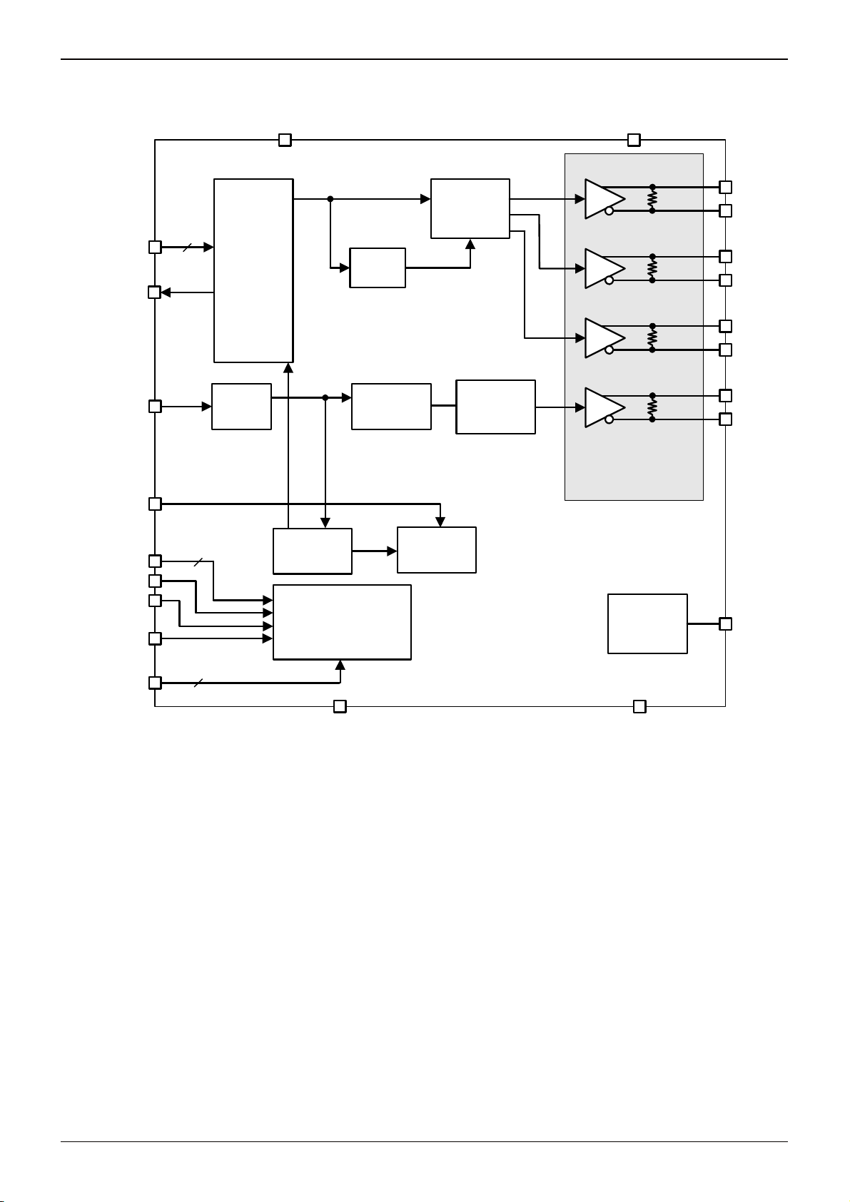
BU7963GUW
●Description
BU7963GUW is a differential serial interface connecting mobile phone LCD modules to the host CPU. Unique technology is
utilized for lower power consumption and EMI. MSDL minimizes the number of wires required - an important consideration
in hinge phones - resulting in greater reliability and design flexibility.
●Features
1) MSDL3 high-speed differential interface with a maximum transfer rate of 1350 Mbps.
2) Compatible with24-bit RGB video mode for LCD controller-to-LCD interface.
3) Pixel clock frequency range from 4 to 45MHz.
4) Depending on the data transfer rate, one, two or three differential data channels can be selected.
●Applications
Serial Interface for LCD Display Interface of Mobile Devices Application.
●Absolute Maximum Ratings:
Parameter Symbol Ratings Unit Remarks
Power Supply Voltage DVDD -0.3 ~ +2.5 V -
MSVDD -0.3 ~ +2.5 V -
Input Voltage VIN -0.3 ~ MSVDD+0.3 V I/O terminals of MSVDD line
-0.3 ~ DVDD+0.3 V I/O terminals of DVDD line
Output Voltage VOUT -0.3 ~ MSVDD+0.3 V I/O terminals of MSVDD line
-0.3 ~ DVDD+0.3 V I/O terminals of DVDD line
Input Current IIN -10 ~ +10 mA -
Output Current IOUT -70 ~ +70 mA -
Preservation Temperature Tstg -55 ~ +125 ℃-
●Operating Conditions:
Parameter Symbol Ratings Unit Conditions
Min Typ Max
Supply Voltage for DVDD VDVDD 1.65 1.80 1.95 V VDVDD = VMSVDD
Supply Voltage for MSVDD VMSVDD 1.65 1.80 1.95 V
Data Transmission Rate DR 120 - 450 Mbps/ch -
Operating Temperature Range Topr -30 25 85 ℃-
No.10058EAT05