Samsung S3F401F Instructions for use

Evaluation Board Manual
S3F401F
16/32-BIT RISC
MICROPROCESSOR
Dec, 2007
REV 1.00

Table of Contents
Chapter 1 Evaluation Board Manual
1. Overview ......................................................................................................................................................1
1.1 Features................................................................................................................................................3
1.2 System Requirements ..........................................................................................................................3
1.3 Board Components...............................................................................................................................4
2. Configuration................................................................................................................................................5
2.1 Detailed Block Configurations...............................................................................................................6
3. Total blocks’ Unit & Jumper Summury.........................................................................................................15
3.1 Function Blocks.....................................................................................................................................15
3.2 Jumper Connection...............................................................................................................................16
3.3 Switches................................................................................................................................................18
4. S3F401F-EVB REV 1.0 Board Schematics .................................................................................................19

EVALUATION BOARD MANUAL S3F401F_BD_UM_REV1.00
1
1 EVALUATION BOARD MANUAL
1. OVERVIEW
S3F401F EVB (Evaluation Board) is a compact platform that is suitable for code development of SAMSUNG's
S3F401F 16-/32-bit RISC microcontroller for an inverter motor and general purpose application.
EVB is consists of several blocks, which can make operate the function of S3F401F. Those functions are from the
followings:
•A 16-/32-bit RISC CPU Core, ARM7TDMI-S
•A built-in 256Kbyte NOR-Flash memory
•An internal 20KB SRAM for stack, data, or code
•An interrupt controller, supporting vectored interrupt
•6xch 16-bit timers with capture and PWM function
•1xch 8-bit basic timer & 3-bit watch-dog timer
•Three programmable I/O port groups
•2xch Inverter motor controller
•2xch 16-bit Encoder counter
•15xch 12-bit ADC
•2xch UART
•2xch SSP
If you need more detail information about S3F401F, meet the samsung web site.
http://www.samsung.com/global/business/semiconductor/productList.do?fmly_id=223

EVALUATION BOARD MANUAL S3F401F_BD_UM_REV1.00
2
BT & WDT
ENC0/1
Crystal or
Ceramic
Oscillator
AHB
ARM7TDMI-S
CORE
SRAM
20KB
FLASH-ROM
256KB
I/O
CONTROLLER
APB
12-BIT ADC
IMC0/1
CLOCK
MONITOR
INTERRUPT
CONTROLLER
ENC0/1IMC0/1
BRIDGE
TAP CONTROLLER
For JTAG
SSP0/1
SSP0/1
UART0/1
UART0/1
Timer0/1/2/3/4/5
Timer0/1/2/3/4/5
Timer0/1/2/3/4/5
Timer0/1/2/3/4/5
TIMER 0/1/2/3/4/5
PLL
Figure 1. S3F401F Block Diagram
EVALUATION BOARD MANUAL S3F401F_BD_UM_REV1.00
3
1.1 FEATURES
Micro-Controller S3F401F, ARM7TDMIS, 16/32-bit RISC Microcontroller
External DC 7~12VBoard Power Source Adjustable voltage regulator out is 3.2V
Board Master Power Switch SW6
Support to protocol for RS-232
Physical interface circuit connected to standard PC through DB9(female)
UART
Interface driver IC MAX3221
Provide SSP, SPI serial communication with external devices (master or slave)
SSP serial EEPROM (8K * 8bit): X25650
Synchronous Serial Port
SSP serial EEPROM (4K * 16bit): 64LC40S
LED IO Port output control display
JTAG Connection 20Way JTAG connector (Multi-ICE Interface, Trace 32 etc.)
1.2 SYSTEM REQUIREMENTS
This section describes the hardware and software system requirements.
ARM Compiler SW
Software Requirements ARM Debugger SW
S3F401F EVB Board Set
Power Supply DC 7~12V ( Recommend Default 12V)
Debugger (Multi-ICE or Trace 32 etc.)
PC(Pentium, 32MB RAM for Windows 95, or 64MB RAM for Windows NT)
COM Port for serial communication
Hardware Requirements
Parallel Port (If using Multi-ICE)

EVALUATION BOARD MANUAL S3F401F_BD_UM_REV1.00
4
1.3 BOARD COMPONENTS
The board consists of the followings.
S3F401F Micro-controller
64LC40S and X25650 as a serial EEPROM for SSP
2 x DSUB Connector for RS-232
2 x Header groups for IMC function
1 x Buzzer
6 x Switches: IRQ x 2, Power, Reset
4 x LED: Power x1, IO Port output x 3
A regulator to generate 3.3V
4MHz Crystal as a master system clock source
Switches for ADC input capacitor selection
7-segment (4-digit) display circuit
A standard 20-pin JTAG interface connector
Dual-line header pins for a port level or signal
53 x Jumpers for function setting control
15 x TP (Test Pole) to check specific pins relating to the digital, analog, PLL power and clock

EVALUATION BOARD MANUAL S3F401F_BD_UM_REV1.00
5
2. CONFIGURATION
S3F401FX
JTAG
POWER BLOCK
Page 1-6
IMC1 HEADER CONNECTOR
Page 1-11
MODE SETTING BLOCK
Page 1-7
UART BLOCK
Page 1-8
IMC0 HEADER CONNECTOR
Page 1-11
Main OSC
7-SEGMENT
Page 1-10
Buzzer
12-bit ADC BLOCK
Page 1 -12
SSP BLOCK
Page 1-9
Figure 2. S3F401F Evaluation Board Top-view

EVALUATION BOARD MANUAL S3F401F_BD_UM_REV1.00
6
2.1 DETAILED BLOCK CONFIGURATIONS
2.1.1 Power Block
5
1
4
2
3
① CN1, CN2, J23: Power Supply Connector
CN1 :VIN
CN2 :GND
J23 :DC adapter connector
② U7: Adjustable Voltage Regulator
3.3V generator JVDD33, VDDCORE, VDDIO
③ SW6: Power Switch
④ DS4: Power Display LED
VDD33 Power-on status display
⑤ J22: JumperSetting
Selection VDDCORE / VDDIO
1-2 connection: The VDD of each block is connected to VDD33.
EVALUATION BOARD MANUAL S3F401F_BD_UM_REV1.00
7
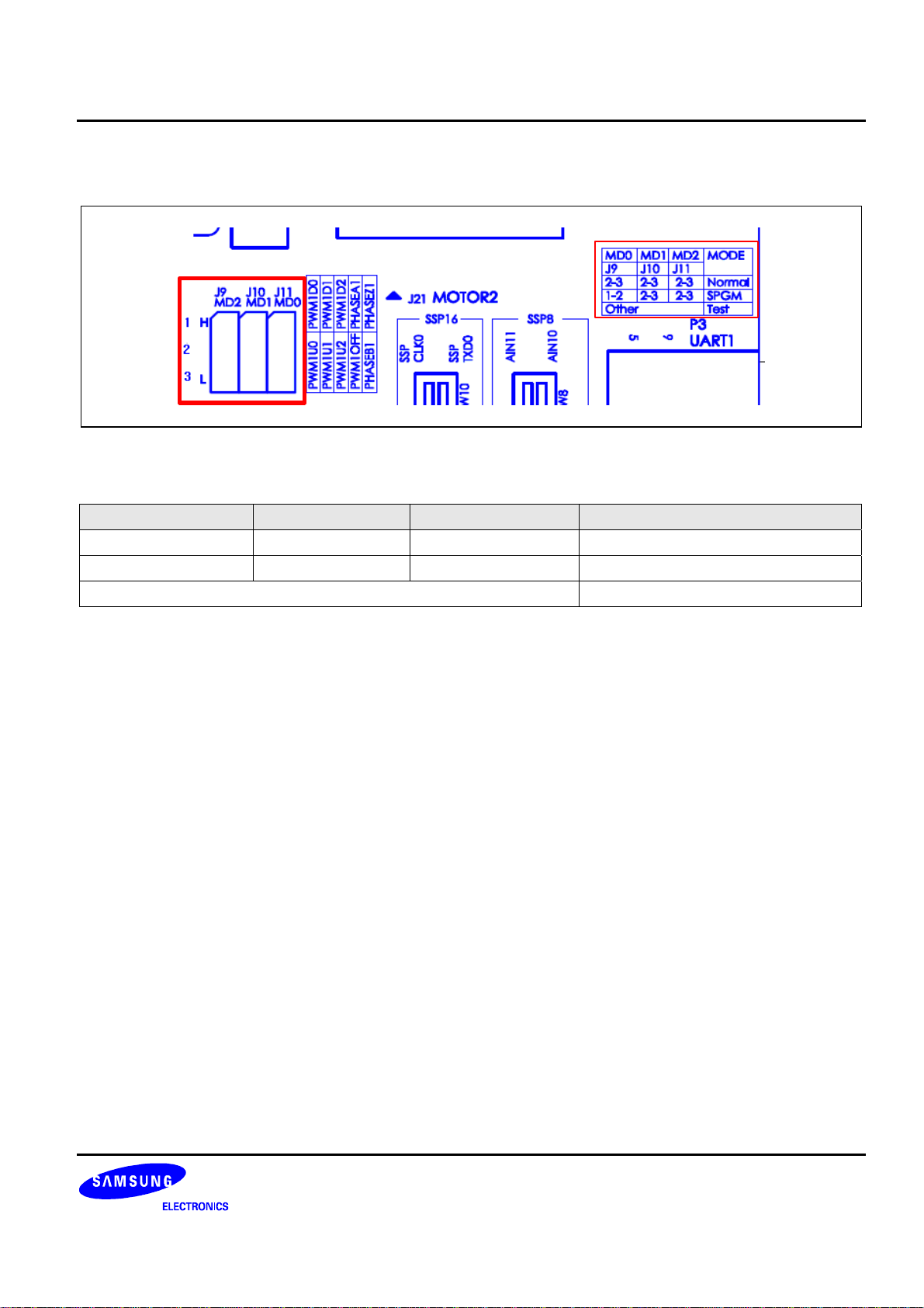
2.1.2 Mode Setting Block
J9 & J10 & J11: Jumper Setting
J9 J10 J11 MD[2:0]
2-3 Connection 2-3 Connection 2-3 Connection NORMAL
1-2 Connection 2-3 Connection 2-3 Connection SPGM
Others Only TEST Mode
EVALUATION BOARD MANUAL S3F401F_BD_UM_REV1.00
8
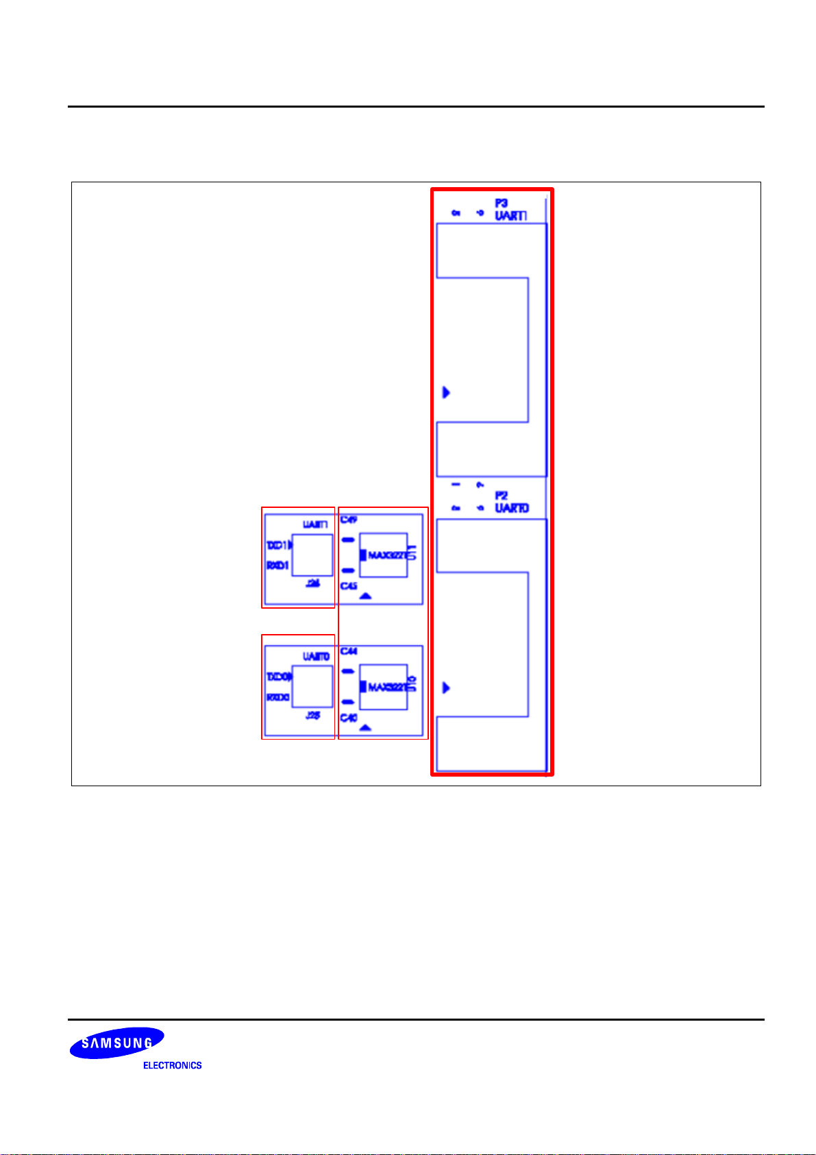
2.1.3 UART Block
1
2
3
④
① U10, U11: UART Driver IC
② P2, P3: UART Connector
③J25 Jumper Setting
TXD0 UARTTXD0 is connected to T1IN of MAX3221.
RXD0 UARTRXD0 is connected to R1OUT of MAX3221.
④J26 Jumper Setting
TXD1 UARTTXD1 is connected to T1IN of MAX3221
RXD1 UARTRXD1 is connected to R1OUT of MAX3221.
Table of contents
Other Samsung Motherboard manuals

Samsung
Samsung UP1500 800-A1 User manual

Samsung
Samsung SyncMaster 710V User manual

Samsung
Samsung API Ultimate Performance UP1100 Instruction Manual

Samsung
Samsung Artik 530 User manual

Samsung
Samsung s3c6410-TFA User manual

Samsung
Samsung AlphaPC 164UX Product manual

Samsung
Samsung AlphaPC 164UX User manual

Samsung
Samsung S3FM02G User manual


