7
SANKEN ELECTRIC CO., LTD.
28103.33
Quasi-Resonant Topology
Primary Switching Regulators
STR-W6756
Because reliability can be affected adversely by improper
storage environments and handling methods, please observe
the following cautions.
Cautions for Storage
• Ensure that storage conditions comply with the standard
temperature (5°C to 35°C) and the standard relative
humidity (around 40% to 75%); avoid storage locations
that experience extreme changes in temperature or
humidity.
• Avoid locations where dust or harmful gases are present
and avoid direct sunlight.
• Reinspect for rust on leads and solderability of the
products that have been stored for a long time.
Cautions for Testing and Handling
When tests are carried out during inspection testing and
other standard test periods, protect the products from
power surges from the testing device, shorts between
the product pins, and wrong connections. Ensure all test
parameters are within the ratings specified by Sanken for
the products.
Remarks About Using Silicone Grease with a Heatsink
• When silicone grease is used in mounting the products on
a heatsink, it shall be applied evenly and thinly. If more
silicone grease than required is applied, it may produce
excess stress.
• Volatile-type silicone greases may crack after long periods
of time, resulting in reduced heat radiation effect. Silicone
greases with low consistency (hard grease) may cause
cracks in the mold resin when screwing the products to a
heatsink.
Our recommended silicone greases for heat radiation
purposes, which will not cause any adverse effect on the
product life, are indicated below:
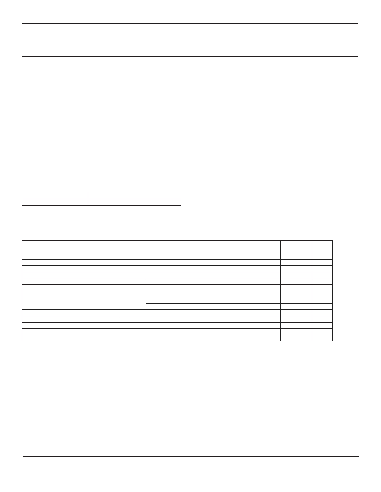
Type Suppliers
G746 Shin-Etsu Chemical Co., Ltd.
YG6260 Momentive Performance Materials Inc.
SC102 Dow Corning Toray Co., Ltd.
Cautions for Mounting to a Heatsink
• When the flatness around the screw hole is insufficient, such
as when mounting the products to a heatsink that has an
extruded (burred) screw hole, the products can be damaged,
even with a lower than recommended screw torque. For
mounting the products, the mounting surface flatness should
be 0.05 mm or less.
• Please select suitable screws for the product shape. Do not
use a flat-head machine screw because of the stress to the
products. Self-tapping screws are not recommended. When
using self-tapping screws, the screw may enter the hole
diagonally, not vertically, depending on the conditions of hole
before threading or the work situation. That may stress the
products and may cause failures.
• Recommended screw torque: 0.588 to 0.785 N●m (6 to 8
kgf●cm).
• For tightening screws, if a tightening tool (such as a driver)
hits the products, the package may crack, and internal
stress fractures may occur, which shorten the lifetime of
the electrical elements and can cause catastrophic failure.
Tightening with an air driver makes a substantial impact.
In addition, a screw torque higher than the set torque can
be applied and the package may be damaged. Therefore, an
electric driver is recommended.
When the package is tightened at two or more places, first
pre-tighten with a lower torque at all places, then tighten
with the specified torque. When using a power driver, torque
control is mandatory.
Soldering
• When soldering the products, please be sure to minimize
the working time, within the following limits:
260±5°C 10±1 s (Flow, 2 times)
380±10°C 3.5±0.5 s (Soldering iron, 1 time)
• Soldering should be at a distance of at least 2.0 mm from
the body of the products.
Electrostatic Discharge
• When handling the products, the operator must be
grounded. Grounded wrist straps worn should have at
least 1 MΩof resistance from the operator to ground to
prevent shock hazard, and it should be placed near the
operator.
• Workbenches where the products are handled should be
grounded and be provided with conductive table and floor
mats.
• When using measuring equipment such as a curve tracer,
the equipment should be grounded.
• When soldering the products, the head of soldering irons
or the solder bath must be grounded in order to prevent
leak voltages generated by them from being applied to the
products.
• The products should always be stored and transported in
Sanken shipping containers or conductive containers, or
be wrapped in aluminum foil.