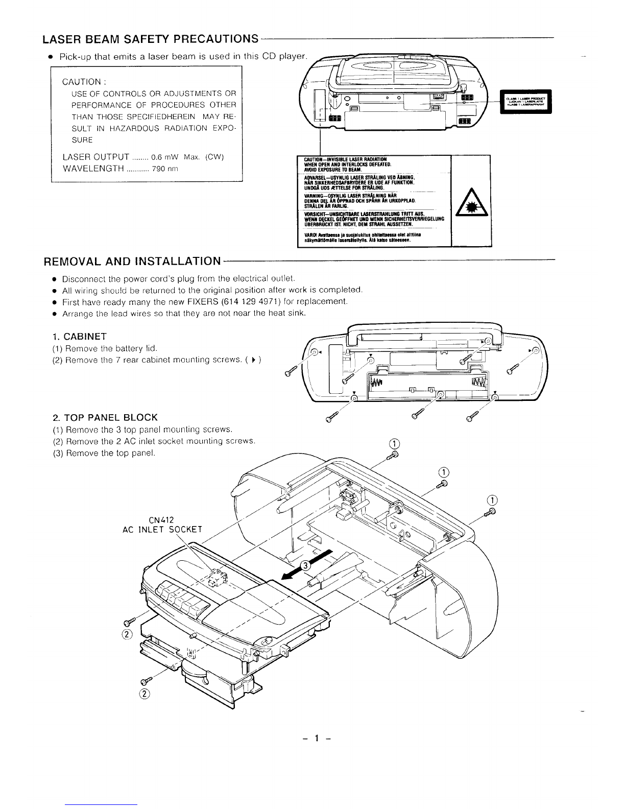
REPLACEMENT OF CD MECHANISM
.Note that the mechanism of the CD player is very delicate.
●It is very important that the spindle motor (which rotates the disc), and the sled motor (which cases the disc signals to be
tracked), as well as the gear and other components, operate smoothly, without eccelen{riclty.
●when handling the pickup, take care not to exert excessive force, and particular care should be taken not to touch the lens
or the drive circuit’s P. W. Board pattern.
1. Replacement of the spindle motor
.First, prepare the new turntable (C M3-2) and new special
washer (C M3-4) for replacement. CM3-2
The removed turntable will be deformed by the heat of the
soldering iron, and cannot be reused. CM3-1
.Prepare dial type calipers.
(l) The attached bonding material can be dissolved by using a
60 Wsoldering iron to heat the shaft at the under part of
the turntable (CM3-2) for about one minute.
(2) The turntable can then be removed from the shaft by very
carefully applying force upward at the center of the lower
surface of the turntable.
(3) Remove the two screws (CM3-3) and remove the spindle CM3-5
motor (CM3-5).
(4) Attach the special washer (CM3-4) to the spindle motor.
(5) Apply asmall amount of amixture of the “Three Bond
2001 and 2015F” bonding materials to the motor’s shaft.
(6) Initial the turntable as shown in the figure. Secure the turn-
table by pressing gently. Be sure to wipe away (by using a
price of cloth, or similar material) any bonding material
coming out of the hole.
Don’t attached bonding mater Ial
at the top of ;haft
IUT I
@
110
iol
\-
i1‘CM2
(SHAFT)
uu
Be sure to w!pe away
the bonding material.
\CH~CK PULLEY
mm
T)
2. Confirm of inclination for the turntable
(l) Connect the digital voltmeter as shown in the figure.
(2) Set the test disc (YEDS 18 =SONY or etc.), press the
PLAY button (Playback for the most inner music). F+ +
(3)At this time, record voltage value to indicate at the digital
voltmeter. 10 kohm
Unit Digital
(4) Access the most outer music, press the PLAY button 0.0033PF Voltmeter
(Playback for the most outer music). A
(5) Again at this time, record voltage value to indicate at the Vc
digital voltmeter. Low Pass Filter
(6) For reference at the recorded voltage of the most inner
music, Confirm at t300 rnV less than for recorded voltage
of the most outer music
-5-


 User manual")