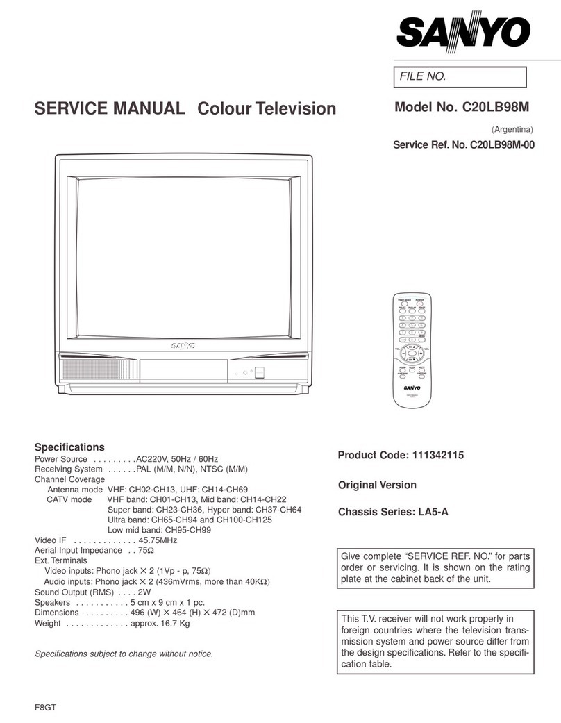
Sanyo C29ZK81 User manual

IFILE NO. I
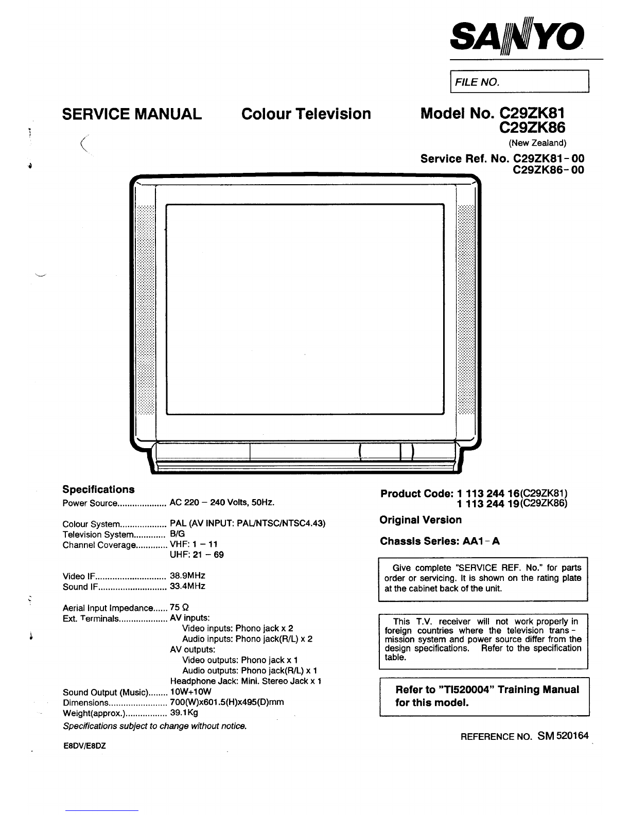
SERVICE MANUAL Colour Television Model No. C29ZK81
“
P(Service Ref.
,.,.,,,.,.,.
,.,.,,,,,,,.
,...........
,...,.,..,,,
,.,.,..,,,.,
,...,.,,,,,,
,.,.,.,,,.,,
............
............
,.,.,,,.,.,.
............
............
............
............
............
............
............
............
............
............
............
,.,.,.,.,.,.
,.,.,.,.,.,.
,.,.,.,.,.,.
,.,.,.,.,.,.
,.,.,.,.,.,.
............
,.,.,.,.,.,.
,.,.,.,.,.,.
,.,.,.,.,.,.
,.,.,.,.,.,.
............
............
............
,.,.,.,.,.,.
,.,.,.,.,.,.
,.,.,.,.,.,.
,.,.,.,.,.,.
............
............
,.,.,.,.,.,.
............
............
,.,.,.,.,.,.
,.,.,.,.,.,.
............
............
............
,.,..,,.,.,.
,,,.,.,.,...
............
,.,,..,.,.,.
............
............
,.,.,.,.,.,.
,,,,,.,.,.,.
,.,.,.,.,.,.
,.,.,.,.,.,.
............
,.,.,.,.,.,.
............
............
............
,.,.,,,.,.,.
.....
............
............
............
............
I I 1\+3
C29ZK86
(New Zealand)
No. C29ZK81 -00
C29ZK86- 00
Specifications Product Code: 1113 24416(C29ZK81)
Power Source .................... AC 220 – 240 Volts, 50 Hz. 1113 24419(C2!W86)
Colour System ................... PAL (AV INPUT: PAL/NTSC/NTSC4.43) Original Version
Television System ............. B/G
Channel Coverage .............VHF: 1 – 11
UHF: 21 – 69
Video IF............................. 38.9 MHz
Sound IF............................ 33.4 MHz
.Aerial Input Impedance ...... 75 S2
Ext. Terminals .................... AV inputs:
~Video inputs: Phono jack x2
Audio inputs: Phono jack(R/L) x2
AV outputs:
Video outputs: Phono jack x1
Audio outputs: Phono jack(R/L) x1
Headphone Jack: Mini. Stereo Jack x1
Sound Output (Music) ........ 10W+l OW
Dimensions ........................ 700(W)X601 .5(H)x495(D)mm
Weight(approx.) ................. 39.1 Kg
Specifications subject to change without notice.
Chassis Series: AAl -A
Give complete “SERVICE REF. No.” for parts
order or servicing. It is shown on the rating plate
at the cabinet back of the unit.
I{
This T.V. receiver will not work properly in
foreign countries where the television trans -
mission system and power source differ from the
design specifications. Refer to the specification
table.
I I
Refer to “T1520004” Training Manuai
for this modei.
REFERENCE NO. SM 520164
E8Dv/E8Dz

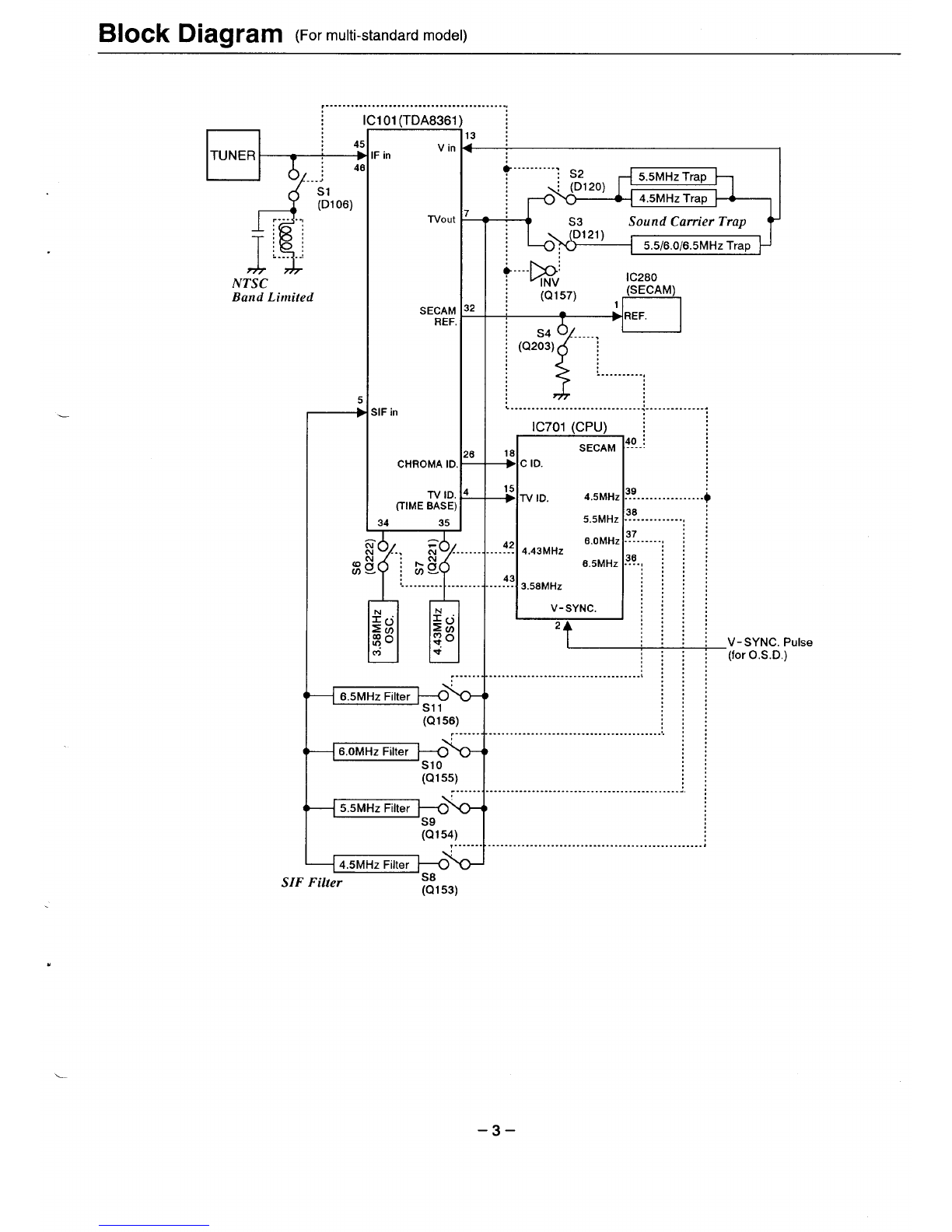
Block Diagram (For multi-standard model)
Note: This block diagram shown is for
full-featured models, other models may
not use the circuits shown. Cl%
V
u
u
r------- ------- ------- ----- i
m1
, , m1-
. . .
>Z=
00.3 m
I_
.-,
L
-------- -- J\\\
>
,------------------
ax
,
-S. *!m ~
. . . . . . . . . . . . . . .
z
4b
:ultig~{
!kkiiio~:
:U)+ S?L:
....... ......
.. ..........
5
:m ~n ;
0s :
:(J)*:
+
... ........
~....= ...........
w
:= ~
.& ZT<
27:”3
--~~~
0>>>
Win-tin
:.-m c.J,-
Cc: .
w: -N-to
mmmm
!- :......... ........
II
Wf)j
>Z
~z< t
mOa
+vl- ,-
,m
..
1
IIJ
I I I
—
—
REAR FRONT <
AV TERMINALS
–2–

Block Diagram (ForMulti-standardModel)
4S1
(D106)
---- --,
I;.. . ..;
NTSC
Band Limited
101 (TDA8361
Fin Vin
Wout
SECAM
REF.
;IF in
CHROMA ID
TV ID.
(TIME BASE)
34 35
7
32
.....W.: :6..
ii
g~ f-s
;uJ-
........... ~~..--c.
s~ +V
~g z(t)
go
q
m+
-------
6.5 MHz Filter +%
Sll
(Q156).......
6,0 MHz Filter
~> Slo
(Q155)
-------
5.5 MHz Filter
~> S9
(Q154)
.......
4.5 MHz Filter J-&w
SIF Filter S8
(Q153)
5.5 MHz Trap
4.5 MHz Trap I
lx
+----:
INV IC280
(SECAM)
(Q157) ,~1
V............
...............................................:
IC701 (CPU) ;
j;
SECAM 40--~
gCID.
~TV ID. 4.5 MHZ ?.?................i
5.5 MHZ 36-----------! !
~,oMHz3?------ !1
42 4.43 MHZ
. . .. . :::
~,5MHz 36-, : : :
:::
::
--4: 3.58 MHZ ::
::
::
V-SYNC. ::
::
2::
:: :.: V-SYNC. Pulse
::: (for O. S. D,)
:::
::::
.................................... :::
,,
.............. ..................................
–3–

Circuit Description
1. POWER SUPPLY
The power supply circuit of the WI -Achassis is
comprises aprimary rectifier smoothing circuit, an
oscillation circuit, acontrol circuit and an output rectifier
circuit.
The AC input voltage is rectified at the double or full-wave
rectifier smoothing circuit, and an unstable DC voltage is
generated at both terminals of the smoothing capacitor
C307. This voltage is supplied to the oscillation circuit,
which is composed of ablocking oscillator circuit that
switches the switching transistor Q313 ON and OFF.
Asquare-wave oscillation is generated in the input
winding according to operation of the control circuit. A
quare-wave with amplitude dependent on the turns ratio of
the input and output windings is obtained in the output
winding. This is rectified in the output rectifier circuit, and
the desired DC voltage is produced.
2. IF& DEFLECTION (TDA8361/8362)
The IF output signal from the tuner passes through the
SAW filter, and it is input to pins 45 and 46ofIC101.
Within the IC, the IF signal passes through the IF
amplifier, video detection and video amplifier circuits, and
is outputted from pin 7as acomposite video signal. In the
monaural model, this composite video signal passes
through the 5.5 MHz(B/G) /6.OMHZ(I) /6.5MHz(D/K) /
4.5 MHz(M) sound bandpass filtering circuit, and it is
inputted into pin5 of IC101. In the stereo model, the SIF
signal is supplied from pin 14 of ICI 81 cTDA2546A> to
pin 5of IC101 through the sound bandpass circuit for
modulation of the main carrier. In the ICI 01, this sound IF
signal passes through the SIF amplifier, FM detector,
external audio switch and audio output circuit, and it is
then outputted from pin 50 as audio drive signal (Monaural
model). In the stereo model, the main audio signal is fed
from pinl to the stereo controller IC1 103(MC44131 PB).
The video signals applied to pins 13 or 15 are separated
into vertical -and horizontal -sync. signals respectively by
the sync. separator in the IC.
The horizontal oscillator requires no external components
and is fully integrated. This oscillator is always running
when the start -pin 36 is supplied with 8V, and the
horizontal drive signal is outputted from pin 37. VR401 is
used for horizontal centring adjustment.
The separated vertical sync. signal from the sync.
separation circuit passes through the vetilcal -separation
circuit, and is applied to trigger divider circuit.
The horizontal oscillation pulse and vertical sync. pulse
are monitored by the trigger divider circuit to select either
the 50Hz or 60Hz system, and automatically adjust the
vertical amplitude.
The output signal from the trigger divider triggers the
vertical oscillator circuit whose external timing
components consist of R402, C401 to pin 42, and the
vertical ramp signal is outputted from pin 43. VR451 is for -
controlling the amount of AC feedback applied to pin 41
for adjustment of the vertical amplitude.
3. VIDEO CHROMA (TDA8361/8362)
The composite video signal output from the pin 7of ICI 01,
passes through Q122, and the sound traps Xl 24, Xl 25,
X126, X127 to reject the sound carrier components, is
then supplied to pin 13 through the equalizing circuit ,
consisting of Q135, Q132 and Q1 34. The external video
signal from SCART or other AV terminals is supplied to
pin 15.
The video signal input to pin 13 or pin 15 is separated into
luminance (Y) signal and chroma signal in IC101. These
pins are also common to the H/V-sync. separation circuit
input already described.
The peaking of Ysignal is adjusted by DC voltage on pin
14.(”SHARPNESS” control)
The chroma signal is divided into R-Y and B-Y chroma
signals, which are demodulated and output from pin 30 (R
-Y) and pin 31 (B -Y). These chroma signals pass
through the 1Hdelay line circuit (IC270), and are re -
inputted at pin 29 (R-Y) and pin 28 (B-Y). These R-Y/B-
Ysignals pass through the RGB matrix circuit and the
RGB selector circuit of IC101. The internal RGB signals
are generated in the RGB matrix circuit and the RGB
selector, consisting of linear amplifiers, clamps and
selects either the internal RGB signals or the external
RGB signals input from pin 22 (R) ,pin 23 (G), pin 24 (B).
Selection is controlled by the voltage at the RGB switch
control (pin 21) and mixed RGB modes are possible since
the RGB switching is fast.
The RGB switch also functions as afast blanking’ pin by
blanking the RGB output stages; here internal and
external RGB signals are overruled.
The RGB signals for the on -screen display are -
superimposed onto the selected RGB signals at the base
of transistors Q21 O, Q211 and Q212 respectively.
The saturation of colour gain is controlled by the DC
voltage of pin 26. (“COLOUR” control)
The contrast control voltage present at pin 25, controls the
RGB signal gain, and the brightness control voltage
present at pin 17, controls DC level of RGB signals.
The RGB signals are finally buffered before being -
presented to the RGB output pins [pin 20 (R), pin 19 (G),
pin 18 (B)].
–4–
Circuit Description
4. AUDIO OUTPUT
4-1 (AN5265)-Monaural model
The audio signal output from pin 50 of ICI 01 is inputted to
pin 2of IC171 and passes through the pre -amplifier
circuit and the drive circuit into the audio amplifier. The
audio amplifier is the SEPP (Single -Ended Push Pull)
type and the output from pin 8drives the speaker directly.
.,. ...
4-2 (TDA7263M)-Stereo model
The audio signals output from pins 17 and 18 of
IC1103(MC44131 PB) are inputted to pins’ 1(Left) and
5(Right) of IC1 102 and passes through the pre -amplifier
circuit and drive circuit, after which it is input to the audio
amplifier. The audio amplifier is the SEPP (single-ended,
push -pull) OTL type and the outputs from pins 8(Right)
and 10(Left) drive the speakers directly.
5. VERTICAL OUTPUT
An LA7833 is used for the vertical output circuit in this
chassis. The vertical ramp signal from pin 43 of IC101 is
inputted to pin 4of IC451. This ramp drives IC451, and
vetilcal scanning is performed. In the first half of scanning
adeflecting current is outputted from pin 2 and passes
through the following path:
VCC(B4) +D451 +pin 3+pin 2+DY +C461 +
vR451/R459.
An electric charge is then stored in C461. In the last half of
scanning the current path is:
C461 +DY +pin 2+pin 1+VR451/R459 +C461
In this way, an increasing sawtooth waveform current
flows directly to the DY to perform electron beam
deflection. During the first half of the blanking period the
vertical ramp signal suddenly turns OFF. Since there is no
longer any current flowing into the DY, the magnetic field
collapses causing an induced current to flow as follows:
DY+ pin 2+ pin 1+VR451/R459+C461 +DY
Once the magnetic field in DY has dissipated, the current
path becomes:
Vcc+ pin 6+ pin 7+ C452apin 34 pin 2Q DY~ C461
@VR451 /R459
and when the prescribed current value is reached, the
vertical drive ramp signal turns ON.
This completes one cycle.
.6. HORIZONTAL OUTPUT
The horizontal oscillation signal is outputted from pin 37 of
IC101 and used to switch the drive transistor Q431. This
●switching signal is current amplified by the drive
transformer T431 and drives the output transistor Q432.
When Q432 turns ON, an increasing current flows directly
to the DY through
C441/C442 +L441/R441 +DY+ Q432- C+Q432- E
and the deflection occurs dun%g the last half of the
Lscanning period. When Q432 turns OFF, the magnetic
field stored in the DY up to that point causes aresonant
current to flow into the capacitors C420 and C423 and
charges them.
The current stored in C420 and C423 then flows back to
the DY causing an opposite magnetic field to be stored in
the DY. This field then collapses increasing acurrent
which switches the dumper diode in Q432 ON. The
resonance state is completed, and an increasing current
then flows again directly to the DY through the dumper
diode.
By this means, the deflection in the first half of the
scanning period is performed. When Q432 turns ON at the
end of the first half of the scanning period, the deflection
during the last half is begun, thus completing one cycle.
In the PCC circuit consisting of Q461 and Q462, the
parabola signal supplied from the vertical circuit is added
at the horizontal output stage and pincushion
compensation is performed by varying the DC bias.
Further, the ABL voltage is fedback to the base of Q462 to
compensate for width variations due to variations in the
beam current.
–5–

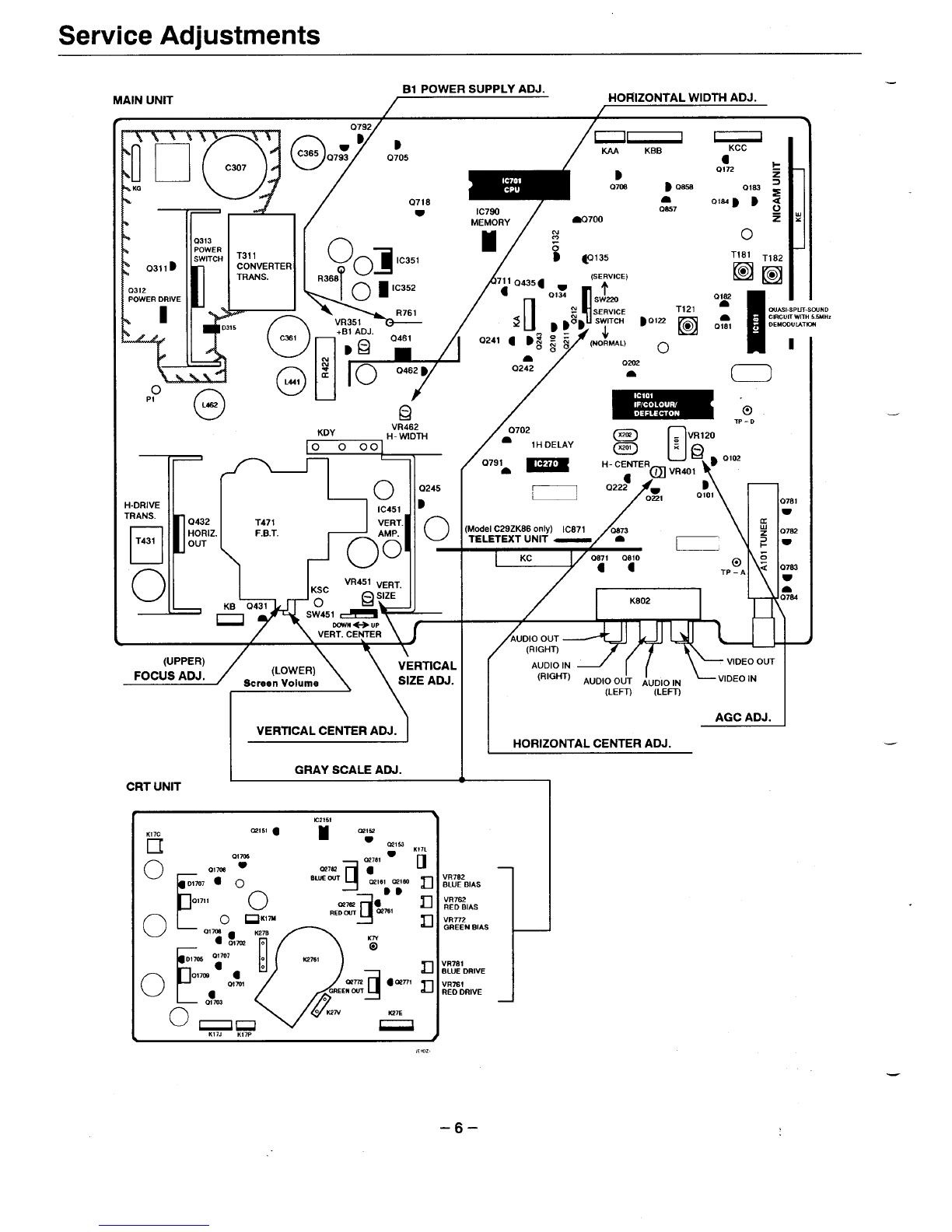
Service Adjustments
MAIN UNIT B1 POWER SUPPLY ADJ. HORIZONTAL WIDTH ADJ.
and’
o~lg II
OUAS!%SPWPSCNND
~cIRcu17WnH 5.~Hz
0181 DEMODUL4TON
1
POWER DRIVE T121
‘o’” la
o
hI14?% =1,1 %i4# “24’:2W’’’MAL)
0202
m
‘@
..-.
/
/
0702
a1HDELAY
—
. .
@3 D
=VR120
B‘B,o,m
‘- c;mER~ VR401
//
0222 B
0% 0101
I-I-DRIVE 1! IIIB
/1K802 I
/II
AUDIO IN
(LEF7)
AGC ADJ.
HORIZONTAL CENTER ADJ.
c
CRT UNIT
CQ151 ●m“;
yK$7L
01705
e
nII
U2781
Olm 02W2 cu
II c11m7 ●oBwE WT C=2161U216TJ m!!%”. . .
—●I
K17C
D
o
0
0)=
%
K2761
mm II●02771
QREENW
J
.
.I(27V W27E
–6–

Service Adjustments
SAFETY PRECAUTIONS :An isolation transformer should be connected in the power line between the receiver and the AC
line before any service is performed on the receiver.
X-RADIATION PRECAUTION The primary source of X-RADIATION in television receiver is the picture tube. The picture
tube is specially constructed to limit X-RADIATION emission. For continued X-RADIATION protection, the replacement tube must
be the same type as the original including suffix letter. Excessive high voltage may produce potentially hazardous X-RADIATION.
To avoid such hazards, the high voltage must be maintain within specified limit. Refer to this service manual for specific high
voltage limits. If high voltage exceeds specified limits, take necessary corrective action. Carefully follow the instructions for +B1 volt
power supply adjustment, and high voltage check to maintain the high voltage within the specified limits.
.
NOTE; Do not attempt this adjustment with weak signal.
(1) Tune the receiver to most clearest (or strongest) VHF
station in your area. Set the brightness and contrast
controls to maximum. Set the colour control to minimum.
(2) Set AGC (VR1 20) control to mid- range.
(3) Turn AGC control in direction which causes snow to appear,
then in the opposite direction until the snow just disappears.
(1) Connect DC meter to R761 (VR351 side) and the ground.
Set the +Bl adjustment control (VR351 )to mid- range.
(2) Set the brightness and contrast to normal.
Tune the receiver to an active channel and synchronized
picture.
(3) Adjust +Bl adjustment control(VR351) for 140 t0.5 volt
DC.
(1) Receive the monochrome circular pattern.
(2) Set the brightness and contrast to normal.
(3) Adjust VR401 for optimum horizontal center position,
Horizontal center
(1) Receive the monochrome circular pattern.
(2) Set the brightness and contrast to normal.
(3) Vertical centering can be adjusted by switching SW451.
ical center
(1) Re:eive the monochrome circular pattern.
(2) Set the brightness and contrast to normal.
(3) Vertical size can be adjusted by using VR451.
rtical size
(1) Receive the monochrome circular pattern.
(2) Set the brightness to normal and contrast to maximum.
(3) Adjust the focus control on the F.B.T for the best focus on
the screen center,
(1) Receiver the monochrome circular pattern.
(2) Set the brightness and the contrast to maximum.
(3) Set the drive volume (VR761 and VR781 )at their
mechanical center.
(4) Set the bias volume (VR762, VR772 and VR782) to
minimum. (fully counter clockwise).
(5) Set the service switch (SW220) to the service side.
(6) Turn the screen volume on the FBT to obtain just visible
one coloured line.
(7) Adjust each bias volume (VR782- blue, VR772- green and
VR762- red) alternately until adim white line produced.
(8) Set the service switch (SW220) to the normal side.
(9) Adjust the drive volume (VR781 -blue and VR761 -red)
alternately to produce normal black and white picture.
(1O)Check for proper grey scale tracking at all brightness
levels.
NOTE : If the grey scale adjustment is made after picturetube
replacement, check high voltage and sub -brightness
adjustment.
(1) Receive the monochrom circular pattern.
(2) Set the brightness and contrast to normal.
(3) If the picture is too wide or narrow, adjust the horizontal
width using VR462.
NOTE: The horiz, width adjustment affects the high voltage,
Therefore, recheck the high voltage,
(1) Connect ahigh voltage probe to anode lead of the picture
tube.
(2) Receive the monochrom circular pattern.
(3) Set the brightness and contrast to maximum.
(4) The high voltage must be between 28-30 t1KV.
NOTE: If the picture tube is replaced, check the high voltage.
-7–

VIF Adjustment
Overall Waveform Adj.
R368(C364 side)
ICI 01- pin48
No band
Item IDetector Adi.
R368(C364 side)
ICI 01- pin48
No band (Q784-Base dGround,
through 1kS2resistor)
TUNER-IF
Q122- Emitter
TP-A
DC 15V
IF AGC(3.5- 4.5V)
BAND
Output Probe
Input Probe
Ground
TUNER-IF
Q122- Emitter
TP-A
100 QDumping Resistor+R124
—SIF System
Sweep ATT.
Output Probe
Oscilloscope Sens.
any
18dB
side a
100mV/DIV
any
18dB
side a
10OmV/DIV
Adjust the overall waveform level
to become 1Vp – p with IF AGC
VOLTAGE.
Adjustment IL
ct
Ivp-p
cP
c’
Waveform
Input Probe
*t
J
T311
CCWVERTER
TRANS.
o
cm Detector Adj.
-a 100 QDumping
Resistor
o
L41
0242 aT
@lF-r)
KDY H- Wmm
Y%
Output Probe
%+.
WM51
KSC
Q:F%T
oSW45+
C431
]a LX3WN~UP
VERT cENTER
MAIN UNIT ‘%% UlO10
WT A“EW3m
ufrn urn
IIC451
@
VERT,
AMP
o
T471
F,8.T
)
(No Band Setting)
–8–

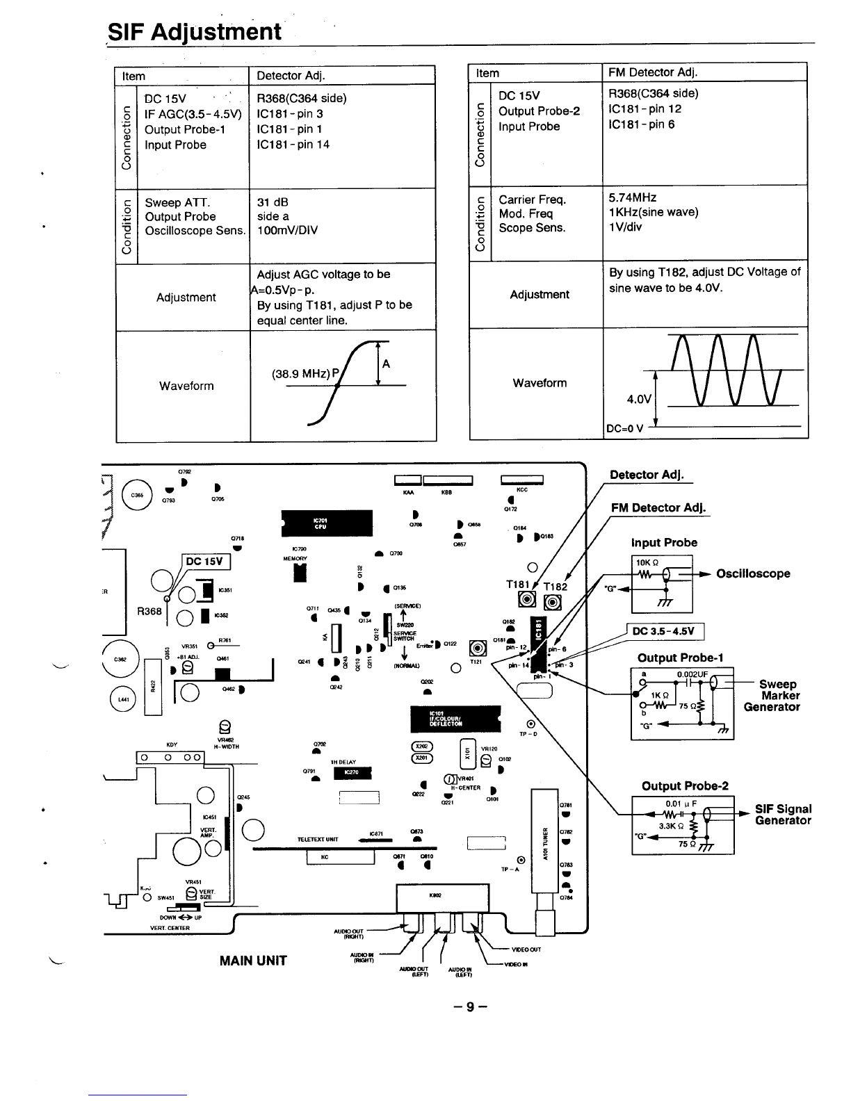
,SIF Adjustment
Item Detector Adj.
13C15V “‘: R368(C364 side)
.6 IF AGC(3.5- 4.5V) IC181 -pin 3
;Output Probe-1 IC181 -pin 1
:Input Probe IC181 -pin 14
s
:Sweep ATT. 31 dB
:~ Output Probe side a
:Oscilloscope Sens. 100mV/DIV
6
Adjust AGC voltage to be
Adjustment A=O.5VP -p.
By using T1 81, adjust Pto be
equal center line.
+
(38.9 MHz) P A
Waveform
wIC791
Item FM Detector Adj.
DC 15V R368(C364 side)
:Output Probe-2 ICI 81- pin 12
gInput Probe ICI 81- pin 6
c
c
s
gCarrier Freq. 5.74 MHZ
:~ Mod. Freq 1KHz(sine wave)
~Scope Sens. 1Vldiv
G
By using T1 82, adjust DC Voltage of
Adjustment sine wave to be 4.OV.
Waveform
@
4.OV
DC=OV
o
L41
●
--l
MEMC%Y
m
On-@
a
I@l
1121
//
o
T161 T1’2
I@@j
0182
ti
a’
0181-
tin- 12
If
G
.-,: :2
w-\
,,.
,,
m!!is5\
@
....
Detector Adj.
FM Detector Ad].
{Input Probe
aosci’’os
Ili%l
+5Q===
Output Probe-1
Output Probe-2
0.01 u F +
3.3K Q
“G-d 75 Q
SIFSignal
Generator
LMAIN UNIT
–9–

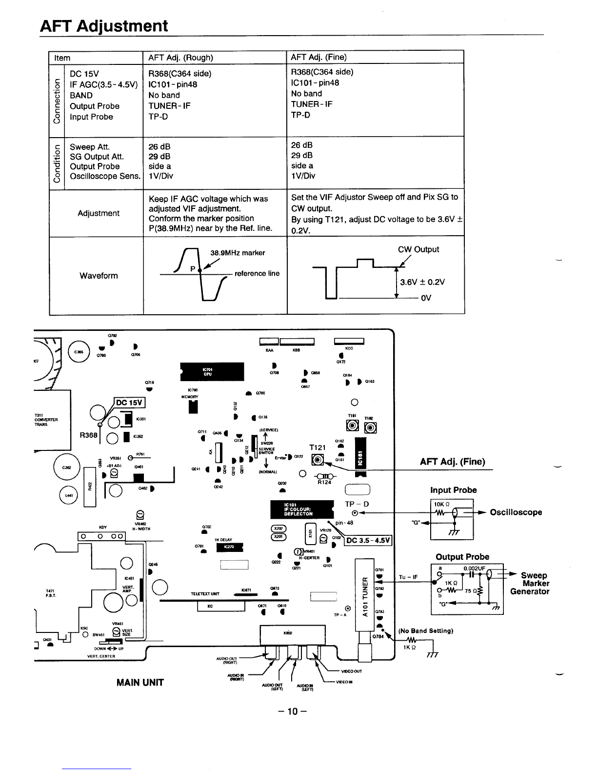
AFT Adjustment
Item AFT Adj. (Rough) AFT Adj. (Fine)
DC 15V R368(C364 side) R368(C364 side)
.; IF AGC(3.5- 4.5V) IC101 -pin48 IC101 -pin48
$1 BAND No band No band
:Output Probe TUNER- IF TUNER- IF
$Input Probe TP-D TP-D
Sweep Att. 26 dB 26 dB
k
:~ SG Output Att. 29 dB 29 dB
:Output Probe side aside a
$Oscilloscope Sens. 1V/Div 1V/Div
Keep IF AGC voltage which was Set the VIF Adjustor Sweep off and Pix SG to
Adjustment adjusted VI Fadjustment. Cw output.
Conform the marker position By using T1 21, adjust DC voltage to be 3.6V f
P(38.9MHz) nearby the Ref. line. 0.2V.
Waveform -*ZLline ,rJ~;v
ox
‘y
oD,
C3W ~: am
ml
~,,, ml!m
T.311
COwEmll
TR4tls.
-i o
C.w
o
L41
FDC 15V
Oz Kx51
’3680 m“w
ic7m
MEMORY a
ca~ n
WA KBB
9
B01n
one B=o,.
*B B 018.3
CU57
Om o
lds-
vR4@
KDY HWIDTH
10 0 00{
1471
FBT
z0782
c~“
~%DOWNeUP
VERT CENTER
AuLm M
MAIN UNIT Auwoul Auwn
mm (Em)
AIT Adj. (Fine)
Input Probe
+Y-tosci’’os’ope
Output Probe
[No Band Setting)
7lKQ
–lo–

PURITY AND CONVERGENCE ADJUSTMENT
CAUTION:The Convergence and Purity adjustments have been made at the factory. Readjustment should be
made only after picture tube or deflection yoke replacement, following the steps below:
PURITY ADJUSTMENT
1.Demagnetize the picture tube and receiver using an external
degaussing coil. When replacing picture tube or deflection
yoke, mount deflection yoke and purity -convergence
magnets assembly properly, see figures 1 and 4.
2.Turn Red and Blue guns off and provide only Green raster,
.Rotate Screen control to fully counterclockwise. Rotate Red
and Blue Bias controls fully counterclockwise. Slowly rotate
Green Bias control clockwise to produce Green raster.
3.Loosen the screw holding the Deflection Yoke and remove
the 3Rubber Wedges, and slide the Deflection Yoke fully
frontward.
4. Rotate and spread the Tabs of the two Purity Magnets to
center the vertical green belt in the picture screen. The Purity
Magnets are also adjusted to obtain vertical centering of the
raster.
L5.SIOWIY slide the Deflection Yoke backward until auniform
green screen is obtained.
6.Check the purity of the red and blue screens for uniformity,
turn off other colours to check this (use bias controls).
Readjust the yoke position if necessary until all screens are
pure.
7.Adiust each Bias control and screen control to obtain white
8. Tighten the mounting screw of the Deflection Yoke. Adjust
Convergence next.
CENTER CONVERGENCE ADJUSTMENT
1.Use adot crosshatch pattern signal.
2. Turn Red and Blue guns on and turn off Green gun, Adjust
the angle between the Tabs of the Four Pole Magnet 1and
2,and superimpose the Red and Blue vertical lines in the
center area of the picture screen. Refer to figure 2.
3. Keeping the mutual angle of the Tabs of the Four Pole
Magnet turn them together to superimpose the Blue and Red
horizontal lines in the center area of the picture screen, Refer
to figure 2.
4. Turn Green gun on and adjust Six Pole Magnet 3 and 4 sthat
the Green line superimposed on the Red/Blue lines.
This is the same procedure used in steps 2 and 3.
Refer to figure 3.
OUTER AREA CONVERGENCE ADJUSTMENT
Slightly loosen the screw holding the Deflection Yoke. Adjust
the Deflection Yoke to converge the detail in the outer area (left
side and right side) of the picture screen by orbital movement of
the front of the Yoke, then secure the Deflection Yoke in
raster. Refer to Gray Scale Adjustment. If part of the picture appropriate position by putting the wedges as illustrated.
screen is coloured, adjust the Deflection Yoke position Tighten screw holding the Deflection Yoke.
forward or backward slightly.
DEFLECTION YOKE
.
FOUR- POLE
MAGNET TABS
rx SIX- POLE
MAGNET TABS
A
Figure- 1. PURITY AND CONVERGENCE MAGNETS
~
Figure- 4. ADJUSTMENT DEFLECTION YOKE
Adjust tabs angle to superimpose Adjust tabs angle to superimpose
blue and red vertical line red/blue and green vertical line
JAdjust tabs together to iAdjust tabs together to
+’
“D\___ ~__~ /:::;%%:;:d
+
GREEN
‘1. __ ~i ~/~~~~~~r;o~’~ne
----
BLUE BLUE/RED
II
Figure- 2BLUE AND RED LINE MOVEMENT Figure-3 BLUE/RED AND GREEN LINE MOVEMENT
–11–

CABINET PARTS LIST
Note :Parts order must contain Service Ref. No., Key No., Parts No., and Description.
Model :C29ZK81/C29ZK86
,.,.,.,.,.,
,.,.,.,,,,, ............
........... ............
,yjj: ............
............
......... ............ y
.,’ ?.5? ,.,.,,,.,.,.
............ ............
........... ,.,.,.,.,.,.
,.,.,.,.,.,. !
‘$ ,.,.,., .,.,. .
............
,.,.,, ,.,, ,, ,.
,.,.,.,., ,,
........... ............ ,,
........... ............ ,,
‘. ........... .
9;::;:: .,..........
............
:,:,:,:,:,: ,.,.,.,.,.,.
,.,.,.,,,,,,
8!............
,.,,,.,,.,,.
,,,,,.,.,.,.
,,,.,.,,,.,.
........... ,,,,,,,.,.,.
........... ,.,.,.,.,.,.
,,,.,,,,,.,.
............
,.,,,,,.,.,.
,.,,,.,.,.,.
,.,,..,.,., ............ >
,.,..,,.,., —
,,,,,.,.,., ............
,,,.,,,.,..
,,,.,...,.,
,.,,,,..,., ml m
............ ml mm =
........... :,:.:,:,:.:, ml 1D
...........
,,,.,.,.,., ,.,.,.,.,.,. .,0
............
,.,.,.,.,.,.
1❑
,,,,,.,.,., I
!Ilmllo
,,,,,,,.,., ............ B❑l
,.,,,.,.,., Mwlnlln
,.,,,,,.,.,
,,,,,,,.,.,
,,,.,,,.,., ............ /
,,,,,.,.,., ,.,.,.,.,.,.
........... ............
..........
,,,,,,,.,.. ............
,,,,,.,.,.. ............
............ 11
,,,,,.,,,.. ,.,.,.,.,.,.
,,,,,,,.,.,
,,,,,,,.,., ,,,.,.,.,.,.
,,,,,.,.,.,.
,,,,,..,,., ,.,.,,,,,.,.
,,,.,,,.,,,
,,,,,.,.,., ,.,.,,,.,.,.
,.,.,.,.,,, ,,,..,,.,.,.
,.,,,,,,,,,.
r
w.
............ 8
,,,,..,..., ......,,,.,, 0
............
,.,.,.,..,,
...........
........... ,..,.,.,.,,,
D
dJc3 C5
.......... .
,.,.,.,.,.,.
,.,,,.,,,.,. AC36A
* . 4..
,
IA ~ !LId
;f ;D
60
.-P.
00A-
Amm
I\11280
,’
,’ \ \ \
7
4SANYO
,’ \\\
54321 l.=
13 ““””u U
./
15 -“-.
‘ey Part No. Description Key
No. No. Part No. IDescription
1. 6102567960 POWERBUTTON 10. 610 256 &lG15 CABINET BACK
6102298406 SPRING ’11” 6102579390 LABEL RATING (C29ZK81 )
2“ 610256 8028 DEC BOARD 6102579406 LABEL RATING (C29ZK86)
—
3. 6102579215 DOOR(C29ZK81) 12. 645011 8180 ASSy,REMOC&IJ)(TF (CZ9ZKB1 )
6102579222 DOOR(C29ZK86) 13. 6102576481 RC-BATTERy LID (C29ZK81)
4. 610 1042505 LATCH PUSH 14. 64tj 008 gIj8g ASSy,REMOCONJXTD (C29ZK86)
5. I610 257 9246 DECCONTROLSHEET 15. 610251 6890 RC-FjATTERyLID (C29ZK86)
6. I610 256 6352 CABINET FRONT
7. 6450039256 BADGE,SANYO 6102564686 INSTRUCT10NS MANUAL
8. 610 258 0860 HANDLE RIGHT ““““-
9I610 258 0877 HANDLE LEFT .
4
–12–

Memory IC (IC790)’ Replacement (Important Note ! )
When Memory IC (IC790) is replaced, it is necessary to make the initializing of IC790 as
following procedure.
[A]Initializing of Memory IC
❑
1Switch off the TV set.
❑
2Replace IC790.
.❑
3Switch on the TV set, and set to the TV mode.
❑
4Press and hold the FUNCTION ~button on the front control panel of the TV set, then press the
RECALL/COLOUR SYSTEM @button on the remote control transmitter.
k+?
P—*
SYSTEM I-A +VPA
(Q)63 @@ Q(3
FLEVEL @COLOUR
11111111111 ---- etc.
V~FUNCTION
.
1
.
COLOUti SYSTEM
❑
5If the setting data is” 1“, select “O” by pressing LEVEL( +or –)~button.
,%
Uuu
-+ PA
A— 0
BASS SUND~kB
00
(4 0
1-LEVEL ITEM-1 SET +O
1
❑
6Press the RECALL/COLOUR SYSTEM@ button to return to the normal TV mode.
.The initializing is now completed.
REMARKS: If there is mistaking the procedure, switch off the TV set and repeat steps (3) to (6).
❑
7Make the channel pre-setting operations to allocate the TV channels (Refer to the instruction manual of this TV set).
–13–

Memory IC (IC790) Replacement (Important Note ! )
[B]Stereo separation setting
❑
1To enter the Service Mode, press and hold the FUNCTION ~button on the front control panel of the
TV set, then press the FUNCTION ~button on the remote control transmitter.
V~FUNCTION
o-
FUNCTION
HSet the service codes and numbers as follows.
u
IADJUST DATA
K1 016
Service Code Service Number
ADJUST DATA
K2 032
@COLOUR
11111111111 ---- etcm
1
ADJUST DATA
KI 000
t
Service Code Service Number
To change the service code, press the FUNCTION button ~.
To change the service number, press the LEVEL (+/– )
button ~.
❑
3Press the RECALL/COLOUR SYSTEM@ button to return to
(_#-Juu
~enormal TV mode.
~RECALL/COLOUR SYSTEM
—
1LEVEL
~Confirm the sound quality with stereo signal receiving.
–14–

.
L
.
.
L
E8DZ
CHASSIS ELECTRICAL PARTS LIST Model :C29ZK86 .
Product safety should be considered when acomponent replacement is made in any area of areceiver.
Components indicated by a~mark in this parts list and the circuit diagram show components whose value have
special significance to product safety. It is particularly recommended that only parts specified on the following parts
list be used for components replacement pointed out by the mark.
Note: Part order must contain Service Ref. No.,Part No..and descriptions. The main PCB unit will be supplied without tuner and
flyback transformer. They shouldbe orderedseparately”.
Read description in the Capacitor and Resister as follows
CAPACITOR
CERAMIC 100P K50V
T T ~=r::;”’’a’e
Less than 1oPF
~: Not specified B:t 0,1 PF
D: i0,5PF Ffl PF
R: +0.25-oPF S: +0- O.25PF
More than 10PF
~: Not smecified B:* O,l%
D: f0.5% Ffl%
H: f3% J: *5%
L: f15% M: *20%
P: +100-0% Q: +30- 10%
u: +75- 10% v: +20- 10%
x: +40- 20% Y: +150-10%
Jria, LRated value: P=pico farad, U=Micro farad
Ceramic..,.., .......Ceramic
MT- PAPER,, ........Metallized Paper
PO LYESTER.,..,.. Polyesterer
MT- POLYEST.,.,.. Metallized Polyester
POLYPRO..,...,.. Polypropylenelene
MT- POLYPRO..,.. Metallized Polypropylene
COMPO FiLM.., .....Composite film
MT- COMPO.,..,.,,.Metallized Cmposite
STYRENE...,,..,..,.. Styrene
TA-SOLID.,..,.. TantalumSolidSolid
AL- SOLID...,,,, AluminiuminiumSolid
ELECT ..................Electrolytic
NP- ELECT,..,..,. NonNon-polarized Electrolytic
OS- SOLID.,,.,..,.., Aluminium Solid with Organic
Semiconductive Electrolytic
DL -ELECT..,..,..,., Double Layered Electrolytic
RE=
CAF
—
Mat
>TOF
ON
—.
rial :
C: f0.25PF
G: t2PF
E: +0-l PF
C: i0,25%
G: f2%
Kf10%
N: t30%
T+50-10%
W:+loo- lo%
Z: +80- 20%
~J Al/4W
T
IL
Rated Wattage
Performance Symbols:
A:General B:Non flammable Z:Low noise
Other :Temperature coefficient
‘Tolerance Symbols
A: t0.05% B: ~0.1% C: f0.25% D: t0,5%
Ki10%
Ffl% G: ~2% J: t5%
M: f20% P+5- 15%
—Rated value, ohms:
K:l ,000, M:l ,000,000
CARBON ,...,,..,..,,.. Carbon
MT- FILM..,,..,,..., ....Metal Film
OXIDE- MT ..,,..,...,. Oxide Metal Film
SOLID ....................Composition
MT- GLAZE ..,,,.,,... Metal Glaze
WIRE WOUND .......Wire Wound
CERAMIC RES..., Ceramicmic
FUSIBLE RES ........Fusible
Ref.No. Part No. Description
610255 1068 ASSY PWB,TEXT(1) E8ET
lhwblOE12400
TRANSISTOR
01001 405011 7305 TR 2SC1740-0
405011 7404 TR 2SC1740-R
405011 7503 TR 2SC1740-S
405011 8401 TR 2SC1740S-0
405011 8500 TR 2SC1740S-R
405011 8609 TR 2SC1740S-S
4050122002 TR 2SC1815-GR
4050122101 TR 2SC1815-O
4050122309 TR 2SC1815-Y
405019 1909 TR 2SC536-E-NP
4050192708 TR 2SC536-F-NP
4050193804 TR 2SC536-G-NP
4050207501 TR 2SC945A-PA
4050207709 TR 2SC945A-OA
4050207907 TR 2SC945A-RA
01002 405011 7305 TR 2SC1740-0
405011 7404 TR 2SC1740-R
405011 7503 TR 2SC1740-S
405011 8401 TR 2SC1740S-0
405011 8500 TR 2SC1740S-R
405011 8609 TR 2SC1740S-S
4050122002 TR 2SC1815-GR
4050122101 TR 2SC1815-O
4050122309 TR 2SC1815-Y
405019 1909 TR 2SC536-E-NP
4050192708 TR 2SC536-F-NP
4050193804 TR 2SC536-G-NP
4050207501 TR 2SC945A-PA
4050207709 TR 2SC945A-OA
4050207907 TR 2SC945A-RA
01003 405011 7305 TR 2SC1740-0
405011 7404 TR 2SC1740-R
405011 7503 TR 2SC1740-S
405011 8401 TR 2SC1740S-O
405011 8500 TR 2SC1740S-R
405011 8609 TR 2SC1740S-S
4050122002 TR 2SC1815-GR
4050122101 TR 2SC1815-O
4050122309 TR 2SC1815-Y
405019 1909 TR 2SC536-E-NP
4050192708 TR 2SC536-F-NP
4050193804 TR 2SC536-G-NP
4050207501 TR 2SC945A-PA
4050207709 TR 2SC945A-OA
4050207907 TR 2SC945A-RA
01007 405011 7305 TR 2SC1740-0
405011 7404 TR 2SC1740-R
405011 7503 TR 2SC1740-S
405011 8401 TR 2SC1740S-O
405011 8500 TR 2SC1740S-R
405011 8609 TR 2SC1740S-S
4050122002 TR 2SC1815-GR
4050122101 TR 2SC1815-O
4050122309 TR 2SC1815-Y
—15—

E8DZ
Ref. No. Part No. Description
405019 1909 TR 2.SC536-E-NP
4050192708 TR 2SC536-F-NP
4050193804 TR 2SC536-G-NP
4050207501 TR 2SC945A-PA
4050207709 TR 2SC945A-OA
4050207907 TR 2SC945A-RA
INTEGRATEDCIRCUIT
IL IUUI
CAPACITOR
Clool
C1OO2
C1OO3
c1004
c1005
C1OO6
C1OO7
C1OO8
C1OO9
Clolo
Cloll
C1012
C1013
RESISTOR
R1OO1
R1OO2
R1003
R1005
R1008
R1011
R1012
R1013
R1014
R1015
R1016
R1018
R102O
R1021
R1029
R103O
:OIL
L1002
IIODE
DI!)02
4UY f!YY 5[UI IL 3AA5Z44AY
403 1666808 MT-POLYEST
4032378007 MT-COMPO
403248 1608 ELECT
4030573107 POLYESTER
403181 8207 POLYESTER
403032 7601 CERAMIC
4030124309 CERAMIC
4030568103 POLYESTER
403 179 3900 POLYESTER
403 1666808 MT-POLYEST
4032378007 MT-COMPO
403 1666808 MT-POLYEST
4032378007 MT-COMPO
4030573107 POLYESTER
403 181 8207 POLYESTER
4030573107 POLYESTER
403 181 8207 POLYESTER
403071 2407 CERAMIC
403071 2407 CERAMIC
403071 2407 CERAMIC
401 0258208
401 0273003
401 0264308
401 0276608
401 0276608
401 0276608
401 0272600
401 0264308
401 0247004
401 0275908
401 026 1307
401 0247400
401 0246700
401 0246700
401 0258208
401 0258208
CARBON
CARBON
CARBON
CARBON
CARBON
CARBON
CARBON
CARBON
CARBON
CARBON
CARBON
CARBON
CARBON
CARBON
CAR80N
CARBON
O.lU J
O.lU J
47U M
O.lU K
O.lU K
8P D
15P J
1000P K
1000P K
O.lU J
O.lU J
O.lU J
O.lU J
O.lU K
O.lU K
O.lU K
O.lU K
1800P K
1800P K
1800P K
22K JA
56K JA
3.3K JA
75 JA
75 JA
75 JA
5.6K JA
3.3K JA
lK JA
68K JA
27K JA
10K JA
100 JA
100 JA
22K JA
22K JA
6450039799 INDUCTOR,3.3UK
4070054505 OIODE DS442X
4080082406 OIOOE 1N4148
63V
50V
16V
50V
50V
50V
50V
50V
50V
63V
50V
63V
50V
50V
50V
50V
50V
50V
50V
50V
1/6W
1/6W
1/6W
1/6W
1/6W
1/6W
1/6W
1/6W
1/6W
1/6W
1/6W
1/6W
1/6W
1/6W
1/6W
1/6W
4070131206 DIODE 1S1555
4070134207 DIODE 1S2076
4070137109 DIODE 1S2473
1ISCELLANEOUS
Xlool 6102496024 CRYSTAL OSCILLATOR
310 255 1624 ASSY PWB,NICAM E8ZV
lAAOh OE12800
rRANSISTOR
0541 405011 7305 TR 2SC1740-11
405011 7404 TR 2SC1740-R
405011 7503 TR 2SC1740-S
Ref. No. Part No. Description
405011 8401 TR 2SC1740S-O
405011 8500 TR 2SC1740S-R
405011 8609 TR 2SC1740S-S
4050122002 TR 2SC1815-GR
4050122101 TR 2SC1815-O
4050122309 TR 2SC1815-Y
405019 1909 TR 2SC536-E-NP
4050192708 TR 2SC536-F-NP
4050193804 TR 2SC536-G-NP
4050207501 TR 2SC945A-PA
4050207709 TR 2SC945A-RA
4050207907 TR 2SC945A-RA
0543 405011 7305 TR 2SC1740-O
405011 7404 TR 2SC1740-R
405011 7503 TR 2SC1740-S
405011 8401 TR 2SC1740S-O
405011 8500 TR 2SC1740S-R
405011 8609 TR 2SC1740S-S
4050122002 TR 2SC1815-GR
4050122101 TR 2SC1815-O
4050122309 TR 2SC1815-Y
405019 1909 TR 2SC536-E-NP
4050192708 TR 2SC536-F-NP
4050193804 TR 2SC536-G-NP
4050207501 TR 2SC945A-PA
4050207709 TR 2SC945A-OA
4050207907 TR 2SC945A-RA
INTEGRATEDCIRCUIT
IC541 4093046006 IC TDA8205
IC542
IC543 4093045900 IC TDA8204
4090268609 IC L78M05-RA
CAPACITOR
C51O
C511
C541
C542
C543
C544
C545
C546
C547
C549
C550
C556
C557
C558
C559
C560
C561
C562
C563
C564
C565
C566
C567
C568
C569
C570
C572
C573
C574
C575
C576
403248 1905
4032481905
4030748901
4030186109
4030186109
4032481905
4030698305
4030698305
4030698305
4030698305
4030698305
403 1666808
4032436806
4030698305
4030750409
4030698305
4030750409
403248 1905
403248 1905
4032086308
403 012 4002
4030750409
403013 1604
403 1668109
4032635704
403011 3402
4030698305
4032481608
403248 1608
4030698305
403248 1608
4031668208
403264 1903
4032583401
ELECT
ELECT
CERAMIC
CERAMIC
CERAMIC
ELECT
CERAMIC
CERAMIC
CERAMIC
CERAMIC
CERAMIC
MT-POLYEST
MT-COMPO
CERAMIC
CERAMIC
CERAMIC
CERAMIC
ELECT
ELECT
ELECT
CERAMIC
CERAMIC
CERAMIC
MT-POLYEST
MT-COMPO
CERAMIC
CERAMIC
ELECT
ELECT
CERAMIC
ELECT
MT-POLYEST
MT-COMPO
ELECT
10UM 16V
10UM 16V
680P K 50V
220P J 50V
220P J 50V
10UM 16V
O.olu z 50V
O.olu z 50V
O.olu z 50V
O.olu z 50V
O.olu z 50V
O.lUJ 63V
O.lUJ 50V
O.olu z 50V
6800P K 50V
O.olu z 50V
6800P K 50V
10UM 16V
10UM 16V
220U M 16V
15P J 50V
6800P K 50V
150P J 50V
0.22U J 63V
0.22U J 50V
120PJ 50V
O.olu z 50V
47UM 16V
47UM 16V
O.olu z 50V
47UM 16V
0.18U J 63V
0.18U J 50V
10UM 25V
C577 4032583401 ELECT 10U M 25V
C578 4030698305 CERAMIC O.olu z 50V
—16—

h3DZ
L
.
‘L
L
,
A
L
Ref.No. PartNo. Description Ref.No. PartNo. Des&i&ion ‘
C579 4030085105 CERAMIC 10P D 50V 4050061707 TR 2SA933S-O
C580 4032441206 ELECT 100UM 10V 4050061806 TR 2SA933S-R
C581 4030854008 NP-ELECT 10UM 16V 0132 4060006804 TR 2SA1015-GR(SAN)
C582 4030854008 NP-ELECT 10UM 16V 405001 7407 TR 2SA1015-0(SAN)
405001 7605 TR 2SA1015-Y(SAN)
RESISTOR 4050043109 TR 2SA564A-O(CU)
R529 401 0254606 CARBON 18K JA l/6W 4050043208 TR 2SA564A-R(CU)
R530 401 0270309 CARBON 47K JA l/6W 4050044205 TR 2SA608-E-CTV-NP
R531 401 0254606 CAR80N 18K JA l/6W 4050044809 TR 2SA608-F-CTV-NP
R532 401 0270309 CARBON 47K JA l/6W 4050061103 TR 2SA933-11
R533 401 0247400 CARBON 10K JA l/6W 4050061202 TR 2SA933-R
R534 401 0278602 CARBON 8.2K JA l/6W 4050061707 TR 2SA933S-O
R535 401 0247400 CARBON 10K JA l/6W 4050061806 TR 2SA933S-R
R536 401 0278602 CARBON 8.2K JA l/6W 0134 4060006804 TR 2SA1015-GR(SAN)
R541 401 0269600 CARBON 470 JA l/6W 405001 7407 TR 2SA1015-O(SAN)
R542 401 0247400 CARBON 10K JA l/6W 405001 7605 TR 2SA1015-Y(SAN)
R543 401 0247400 CARBON 10K JA l/6W 4050043109 TR 2SA564A-13(CU)
R544 401 025 1605 CARBON 1.5KJA l/6W 4050043208 TR 2SA564A-R(CU)
R545 401 0246700 CARBON 100 JA l/6W 4050044205 TR 2SA608-E-CTV-NP
R546 401 0260607 CARBON 270 JA l/6W 4050044809 TR 2SA608-F-CTV-NP
R547 401 0260409 CARBON 27 JA l/6W 405006 1103 TR 2SA933-O
R548 401 0269303 CARBON 47 JA l/6W 4050061202 TR 2SA933-R
R549 401 0275205 CARBON 680 JA l/6W 405006 1707 TR 2SA933S-O
R559 401 0272600 CARBON 5.6K JA l/6W 405006 1806 TR 2SA933S-R
R560 401 0269006 CARBON 43K JA l/6W 0135 405011 7305 TR 2SC1740-R
R561 401 0254606 CARBON 18K JA l/6W 405011 7404 TR 2SC1740-R
R562 401 0269006 CARBON 43K JA l/6W 405011 7503 TR 2SC1740-S
R563 401 0272600 CARBON 5.6K JA l/6W 405011 8401 TR 2SC1740S+I
R564 401 0260607 CARBON 270 JA l/6W 405011 8500 TR 2SC1740S-R
R565 401 0267408 CARBON 39K JA l/6W 405011 8609 TR 2SC1740S-S
R566 401 0129904 CARBON 10M JA l/4W 4050122002 TR 2SC1815-GR
R5F7 401 025 1308 CARBON 150 JA l/6W 4050122101 TR 2SC1815-O
R568 401 0246700 CARBON 100 JA l/6W 4050122309 TR 2SC1815-Y
R569 401 0246700 CAR80N 100 JA l/6W 405019 1909 TR 2SC536-E-NP
R570 401 0248001 CARBON lMJA l/6W 4050192708 TR 2SC536-F-NP
R571 401 0272600 CARBON 5.6K JA l/6W 4050193804 TR 2SC536-G-NP
R572 401 0669103 OXIDE-MT 27 JA 2W 4050207501 TR 2SC945A-PA
4050207709 TR 2SC945A-OA
TRANSFORMER 4050207907 TR 2SC945A-RA
T541 6102086089 S BLOCK 0172 405011 7305 TR 2SC1740-O
405011 7404 TR 2SC1740-R
COIL 405011 7503 TR 2SC1740-S
L541 645011 0252 INDUCTOR,2.2UK 405011 8401 TR 2SC1740S-O
L542 645011 0252 INDUCTOR,2.2UK 405011 8500 TR 2SC1740S-R
L543 645011 0252 INDUCTOR,2.2UK405011 8609 TR 2SC1740S-S
L544 645011 0252 INDUCTOR,2.2UK4050122002 TR 2SC1815-GR
L547 6450082894 INOUCTOR,5.6UK4050122101 TR 2SC1815-O
4050122309 TR 2SC1815-Y
MISCELLANEOUS 4050191909 TR 2SC536-E-NP
K5A 6450050077 SOCKET,PWB-PWB15P 4050192708 TR 2SC536-F-NP
X541 6100152854 TRAP,CERAMIC5.5MHZ 4050193804 TR 2SC536-G-NP
X543 6102330649 CRYSTALOSCILLATOR 4050207501 TR 2SC945A-PA
6102579123 ASSY PWB,MAIN E8DZ 4050207709 TR 2SC945A-OA
lAAOblOE18200 4050207907 TR 2SC945A-RA
0181 405011 7305 TR 2SC1740-11
405011 7404 TR 2SC1740-R
TRANSISTOR 405011 7503 TR 2SC1740-S
0101 4050133305 TR 2SC2216(SAN) 405011 8401 TR 2SC1740S-O
0102 4050166204 TR 2SC3000-D 405011 8500 TR 2SC1740S-R
4050166402 TR 2SC3000-E 405011 8609 TR 2SC1740S-S
4050166600 TR 2SC3000-F 4050122002 TR 2SC1815-GR
0122 4060006804 TR 2SA1015-GR(SAN) 4050122101 TR 2SC1815-O
405001 7407 TR 2sA1015-o(SAN) 4050122309 TR 2SC1815-Y
405001 7605 TR 2SA1015-Y(SAN) 405019 1909 TR 2SC536-E-NP
4050043109 TR 2SA564A-O(CU) 4050192708 TR 2SC536-F-NP
4050043208 TR 2SA564A-R(CU) 4050193804 TR 2SC536-G-NP
4050044205 TR 2SA608-E-CTV-NP 4050207501 TR 2SC945A-PA
4050044809 TR 2SA608-F-CTV-NP 4050207709 TR 2SC945A-OA
405006 1103 TR 2SA933-O 4050207907 TR 2SC945A-RA
405006 1202 TR 2SA933-R 0182 405011 7305 TR 2SC1740-0
—17—

E8DZ
Ref. No. IPart No. Description
0183
0184
0202
0210
—.—
405011 7404
405011 7503
405011 8401
405011 8500
405011 8609
405012 2002
4050122101
4050122309
405019 1909
4050192708
4050193804
4050207501
4050207709
4050207907
405011 7305
405011 7404
405011 7503
405011 8401
405011 8500
405011 8609
4050122002
4050122101
4050122309
4050191909
4050192708
4050193804
4050207501
4050207709
4050207907
405011 7305
405011 7404
405011 7503
405011 8401
405011 8500
405011 8609
4050122002
4050122101
4050122309
405019 1909
4050192708
4050193804
4050207501
4050207709
4050207907
405011 7305
405011 7404
405011 7503
405011 8401
405011 8500
405011 8609
4050122002
4050122101
4050122309
405019 1909
4050192708
4050193804
4050207501
4050207709
4050207907
4060006804
405001 7407
405001 7605
4050043109
4050043208
4050044205
4050044809
4050061103
405006 1202
4050061707
4050061806
TR 2SC1740-R
TR 2SC1740-S
TR 2SC1740S-O
TR 2SC1740S-R
TR 2SC1740S-S
TR 2SC1815-GR
TR 2SC1815-O
TR 2SC1815-Y
TR 2SC536-E-NP
TR 2SC536-F-NP
TR 2SC536-G-NP
TR 2SC945A-PA
TR 2SC945A-OA
TR 2SC945A-RA
TR 2SC1740-O
TR 2SC1740-R
TR 2SC1740-S
TR 2SC1740S-O
TR 2SC1740S-R
TR 2SC1740S-S
TR 2SC1815-GR
TR 2SC1815-O
TR 2SC1815-Y
TR 2SC536-E-NP
TR 2SC536-F-NP
TR 2SC536-G-NP
TR 2SC945A-PA
TR 2SC945A-OA
TR 2SC945A-RA
TR 2SC1740-O
TR 2SC1740-R
TR 2SC1740-S
TR 2SC1740S-O
TR 2SC1740S-R
TR 2SC1740S-S
TR 2SC1815-GR
TR 2SC1815-O
TR 2SC1815-Y
TR 2SC536-E-NP
TR 2SC536-F-NP
TR 2SC536-G-NP
TR 2SC945A-PA
TR 2SC945A-OA
TR 2SC945A-RA
TR 2SC1740-O
TR 2SC1740-R
TR 2SC1740-S
TR 2SC1740S-O
TR 2SC1740S-R
TR 2SC1740S-S
TR 2SC1815-GR
TR 2SC1815-O
TR 2SC1815-Y
TR 2SC536-E-NP
TR 2SC536-F-NP
TR 2SC536-G-NP
TR 2SC945A-PA
TR 2SC945A-OA
TR 2SC945A-RA
TR 2SA1015-GR(SAN)
TR 2SA1015-0(SAN)
TR 2SA1015-Y(SAN)
TR 2SA564A-O(CU)
TR 2SA564A-R(CU)
TR 2SA608-E-CTV-NP
TR 2SA608-F-CTV-NP
TR 2SA933-O
TR 2SA933-R
TR 2SA933S-O
TR 2SA933S-R
Ref. No. Part No. Description
0211
0212
0221
0222
0241
0242
4060006804
405001 7407
405001 7605
4050043109
4050043208
4050044205
4050044809
405006 1103
405006 1202
405006 1707
405006 1806
4060006804
405001 7407
405001 7605
4050043109
4050043208
4050044205
4050044809
405006 1103
405006 1202
4050061707
4050061806
4060006804
405001 7407
405001 7605
4050043109
4050043208
4050044205
4050044809
4050061103
405006 1202
405006 1707
405006 1806
4060006804
405001 7407
405001 7605
4050043109
4050043208
4050044205
4050044809
405006 1103
405006 1202
405006 1707
405006 1806
405011 7305
405011 7404
405011 7503
405011 8401
405011 8500
405011 8609
4050122002
4050122101
4050122309
405019 1909
4050192708
4050193804
4050207501
4050207709
4050207907
4060006804
405001 7407
405001 7605
4050043109
4050043208
4050044205
4050044809
4050061103
405006 1202
4050061707
405006 1806
TR 2SA1015-GR(SAN)
TR 2SA1015-0(SAN)
TR 2SA1015-Y(SAN)
TR 2SA564A-O(CU)
TR 2SA564A-R(CU)
TR 2SA608-E-CTV-NP
TR 2SA608-F-CTV-NP
TR 2SA933-O
TR 2SA933-R
TR 2SA933S-O
TR 2SA933S-R
TR 2SA1015-GR(SAN)
TR 2SA1015-0(SAN)
TR 2SA1015-Y(SAN)
TR 2SA564A-O(CU)
TR 2SA564A-R(CU)
TR 2SA608-E-CTV-NP
TR 2SA608-F-CTV-NP
TR 2SA933-O
TR 2SA933-R
TR 2SA933S-O
TR 2SA933S-R
TR 2SA1015-GR(SAN)
TR 2SA1015-0(SAN)
TR 2SA1015-Y(SAN)
TR 2SA564A-O(CU)
TR 2SA564A-R(CU)
TR 2SA608-E-CTV-NP
TR 2SA608-F-CTV-NP
TR 2SA933-O
TR 2SA933-R
TR 2SA933S-O
TR 2SA933S-R
TR 2SA1015-GR(SAN)
TR 2SA1015-0(SAN)
TR 2SA1015-Y(SAN)
TR 2SA564A-O(CU)
TR 2SA564A-R(CU)
TR 2SA608-E-CTV-NP
TR 2SA608-F-CTV-NP
TR 2SA933-O
TR 2SA933-R
TR 2SA933S-O
TR 2SA933S-R
TR 2SC1740-O
TR 2SC1740-R
TR 2SC1740-S
TR 2SC1740S-O
TR 2SC1740S-R
TR 2SC1740S-S
TR 2SC1815-GR
TR 2SC1815-O
TR 2SC1815-Y
TR 2SC536-E-NP
TR 2SC536-F-NP
TR 2SC536-G-NP
TR 2SC945A-PA
TR 2SC945A-OA
TR 2SC945A-RA
TR 2SA1015-GR(SAN)
TR 2SA1015-O(SAN)
TR 2SA1015-Y(SAN)
TR 2SA564A-O(CU)
TR 2SA564A-R(CU)
TR 2SA608-E-CTV-NP
TR 2SA608-F-CTV-NP
TR 2SA933-O
TR 2SA933-R
TR 2SA933S-O
TR 2SA933S-R
—18—

“E8DZ
.
.
w
,
.
L
Ref. No. IParl No. IDescription
0243
0245
0311
0312
0313
0353
0431
0432
0435
4060006804 TR 2SA1015-GR(SAN)
405001 7407 TR 2SA1015-0(SAN)
405001 7605 TR 2SA1015-Y(SAN)
4050043109 TR 2SA564A-O(CU)
4050043208 TR 2SA564A-R(CU)
4050044205 TR 2SA608-E-CTV-NP
4050044809 TR 2SA608-F-CTV-NP
405006 1103 TR 2SA933-O
405006 1202 TR 2SA933-R
405006 1707 TR 2SA933S-O
405006 1806 TR 2SA933S-R
405011 7305 TR 2SC1740-O
405011 7404 TR 2SC1740-R
405011 7503 TR 2SC1740-S
405011 8401 TR 2SC1740S-O
405011 8500 TR 2SC1740S-R
405011 8609 TR 2SC1740S-S
4050122002 TR 2SC1815-GR
405 0122101 TR 2SC1815-O
4050122309 TR 2SC1815-Y
405 019 1909 TR 2SC536-E-NP
4050192708 TR 2SC536-F-NP
4050193804 TR 2SC536-G-NP
405 0207501 TR 2SC945A-PA
405 0207709 TR 2SC945A-OA
405 0207907 TR 2SC945A-RA
4060006804 TR 2SA1015-GR(SAN)
405001 7407 TR 2SA1015-0(SAN)
405001 7605 TR 2SA1015-Y(SAN)
4050043109 TR 2SA564A-O(CU)
4050043208 TR 2SA564A-R(CU)
4050044205 TR 2SA608-E-CTV-NP
4050044809 TR 2SA608-F-CTV-NP
405006 1103 TR 2SA933-O
405006 1202 TR 2SA933-R
405006 1707 TR 2SA933S-O
405006 1806 TR 2SA933S-R
4050580208 TR 2SC3807-R-CTV-YA
4050950407 TR 2SC4429-L-YB
4050950308 TR 2SC4429-M-YB
405011 7305 TR 2SC1740-O
405011 7404 TR 2SC1740-R
405011 7503 TR 2SC1740-S
405011 8401 TR 2SC1740S-O
405011 8500 TR 2SC1740S-R
405011 8609 TR 2SC1740S-S
4050122002 TR 2SC1815-GR
4050122101 TR 2SC1815-O
4050122309 TR 2SC1815-Y
405019 1909 TR 2SC536-E-NP
4050192708 TR 2SC536-F-NP
4050193804 TR 2SC536-G-NP
4050207501 TR 2SC945A-PA
4050207709 TR 2SC945A-OA
4050207907 TR 2SC945A-RA
4050180507 TR 2SC3332-R
4050180606 TR 2SC3332-S
4050822407 TR 2SD1879-CTV-Y8
4060006804 TR 2SA1015-GR(SAN)
405001 7407 TR 2SA1015-O(SAN)”
405001 7605 TR 2SA1015-Y(SAN)
4050043109 TR 2SA564A-O(CU)
4050043208 TR 2SA564A-R(CU)
4050044205 TR 2SA608-E-CTV-NP
4050044809 TR 2SA608-F-CTV-NP
405006 1103 TR 2SA933-O
405006 1202 TR 2SA933-R
405006 1707 TR 2SA933S-O
405006 1806 TR 2SA933S-R
0461 4050647307 TR 2SB1274-O-RA
Ref.No. I partNo. I Description
4050647406
4050647505
0462 405011 7305
405011 7404
405011 7503
405011 8401
405011 8500
405011 8609
4050122002
4050122101
4050122309
405019 1909
4050192708
4050193804
4050207501
4050207709
4050207907
0700 405011 7305
405011 7404
405011 7503
405011 8401
405011 8500
405011 8609
4050122002
4050122101
4050122309
4050191909
4050192708
4050193804
4050207501
4050207709
4050207907
0702 405011 7305
405011 7404
405011 7503
405011 8401
405011 8500
405011 8609
4050122002
4050122101
4050122309
405019 1909
4050192708
4050193804
4050207501
4050207709
4050207907
0708 4060006804
405001 7407
405001 7605
4050043109
4050043208
4050044205
4050044809
405006 1103
405006 1202
4050061707
4050061806
0711 405 1184207
0718 405011 7305
405011 7404
405011 7503
405011 8401
405011 8500
405011 8609
4050122002
4050122101
4050122309
405019 1909
4050192708
TR 2SB1274-R-RA
TR 2SB1274-S-RA
TR 2SC1740-O
TR 2SC1740-R
TR 2SC1740-S
TR 2SC1740S-O
TR 2SC1740S-R
TR 2SC1740S-S
TR 2SC1815-GR
TR 2SC1815-O
TR 2SC1815-Y
TR 2SC536-E-NP
TR 2SC536-F-NP
TR 2SC536-G-NP
TR 2SC945A-PA
TR 2SC945A-OA
TR 2SC945A-RA
TR 2SC1740-O
TR 2SC1740-R
TR 2SC1740-S
TR 2SC1740S-O
TR 2SC1740S-R
TR 2SC1740S-S
TR 2SC1815-GR
TR 2SC1815-O
TR 2SC1815-Y
TR 2SC536-E-NP
TR 2SC536-F-NP
TR 2SC536-G-NP
TR 2SC945A-PA
TR 2SC945A-OA
TR 2SC945A-RA
TR 2SC1740-O
TR 2SC1740-R
TR 2SC1740-S
TR 2SC1740S-O
TR 2SC1740S-R
TR 2SC1740S-S
TR 2SC1815-GR
TR 2SC1815-O
TR 2SC1815-Y
TR 2SC536-E-NP
TR 2SC536-F-NP
TR 2SC536-G-NP
TR 2SC945A-PA
TR 2SC945A-OA
TR 2SC945A-RA
TR 2SA1015-GR(SAN)
TR 2SA1015-0(SAN)
TR 2SA1015-Y(SAN)
TR 2SA564A-O(CU)
TR 2SA564A-R(CU)
TR 2SA608-E-CTV-NP
TR 2SA608-F-CTV-NP
TR 2SA933-CI
TR 2SA933-R
TR 2SA933S-O
TR 2SA933S-R
TR PH2369
TR 2SC1740-O
TR 2SC1740-R
TR 2SC1740-S
TR 2SC1740S-O
TR 2SC1740S-R
TR 2SC1740S-S
TR 2SC1815-GR
TR 2SC1815-O
TR 2SC1815-Y
TR 2SC536-E-NP
TR 2SC536-F-NP
—19—

E8DZ
Ref. No. IPart No. IDescription
0781
0782
0783
0784
0791
0792
4050193804 TR 2SC536-G-NP
4050207501 TR 2SC945A-PA
4050207709 TR 2SC945A-OA
4050207907 TR 2SC945A-RA
4060006804 TR 2SA1015-GR(SAN)
405001 7407 TR 2SA1015-0(SAN)
405001 7605 TR 2SA1015-Y(SAN)
4050043109 TR 2SA564A-O(CU)
4050043208 TR 2SA564A-R(CU)
4050044205 TR 2SA608-E-CTV-NP
4050044809 TR 2SA608-F-CTV-NP
405006 1103 TR 2SA933-O
405006 1202 TR 2SA933-R
405006 1707 TR 2SA933S-O
4050061806 TR 2SA933S-R
4060006804 TR 2SA1015-GR(SAN)
405001 7407 TR 2SA1015-0(SAN)
405001 7605 TR 2SA1015-Y(SAN)
4050043109 TR 2SA564A-O(CU)
4050043208 TR 2SA564A-R(CU)
4050044205 TR 2SA608-E-CTV-NP
4050044809 TR 2SA608-F-CTV-NP
405006 1103 TR 2SA933-O
405006 1202 TR 2SA933-R
405006 1707 TR 2SA933S-O
405006 1806 TR 2SA933S-R
405011 7305 TR 2SC1740-O
405011 7404 TR 2SC1740-R
405011 7503 TR 2SC1740-S
405011 8401 TR 2SC1740S-O
405011 8500 TR 2SC1740S-R
405011 8609 TR 2SC1740S-S
4050122002 TR 2SC1815-GR
4050122101 TR 2SC1815-O
4050122309 TR 2SC1815-Y
405019 1909 TR 2SC536-E-NP
4050192708 TR 2SC536-F-NP
4050193804 TR 2SC536-G-NP
4050207501 TR 2SC945A-PA
4050207709 TR 2SC945A-OA
4050207907 TR 2SC945A-RA
405011 7305 TR 2SC1740-O
405011 7404 TR 2SC1740-R
405011 7503 TR 2SC1740-S
405011 8401 TR 2SC1740S-O
405011 8500 TR 2SC1740S-R
405011 8609 TR 2SC1740S-S
4050122002 TR 2SC1815-GR
4050122101 TR 2SC1815-O
4050122309 TR 2SC1815-Y
405019 1909 TR 2SC536-E-NP
4050192708 TR 2SC536-F-NP
405019 3804 TR 2SC536-G-NP
4050207501 TR 2SC945A-PA
4050207709 TR 2SC945A-OA
4050207907 TR 2SC945A-RA
405011 7305 TR 2SC1740-O
405011 7404 TR 2SC1740-R
405011 7503 TR 2SC1740-S
Ref. No.
0793
0810
0857
0858
0871
Part No. Description
405011 8401 TR 2SC1740S-O
405011 8500 TR 2SC1740S-R
405011 8609 TR 2SC1740S-S
4050122002 TR 2SC1815-GR
4050122101 TR 2SC1815-O
4050122309 TR 2SC1815-Y
405019 1909 TR 2SC536-E-NP
4050192708 TR 2SC536-F-NP
4050193804 TR 2SC536-G-NP
4050207501 TR 2SC945A-PA
4050207709 TR 2SC945A-OA
4050207907 TR 2SC945A-RA
405011 7305 TR 2SC1740-O
405011 7404 TR 2SC1740-R
405011 7503 TR 2SC1740-S
405011 8401 TR 2SC1740S-O
405011 8500 TR 2SC1740S-R
405011 8609 TR 2SC1740S-S
4050122002 TR 2SC1815-GR
4050122101 TR 2SC1815-O
4050122309 TR 2SC1815-Y
405019 1909 TR 2SC536-E-NP
4050192708 TR 2SC536-F-NP
4050193804 TR 2SC536-G-NP
4050207501 TR 2SC945A-PA
4050207709 TR 2SC945A-OA
4050207907 TR 2SC945A-RA
405011 7305 TR 2SC1740-O
405011 7404 TR 2SC1740-R
405011 7503 TR 2SC1740-S
405011 8401 TR 2SC1740S-O
405011 8500 TR 2SC1740S-R
405011 8609 TR 2SC1740S-S
4050122002 TR 2SC1815-GR
4050122101 TR 2SC1815-O
4050122309 TR 2SC1815-Y
4050191909 TR 2SC536-E-NP
4050192708 TR 2SC536-F-NP
4050193804 TR 2SC536-G-NP
4050207501 TR 2SC945A-PA
4050207709 TR 2SC945A-OA
4050207907 TR 2SC945A-RA
4060006804 TR 2SA1015-GR(SAN)
405001 7407 TR 2SA1015-0(SAN)
405001 7605 TR 2SA1015-Y(SAN)
4050043109 TR 2SA564A-O(CU)
4050043208 TR 2SA564A-R(CU)
4050044205 TR 2SA608-E-CTV-NP
4050044809 TR 2SA608-F-CTV-NP
4050061103 TR 2SA933-O
405006 1202 TR 2SA933-R
4050061707 TR 2SA933S-O
405006 1806 TR 2SA933S-R
405011 7305 TR 2SC1740-O
405011 7404 TR 2SC1740-R
—20—
This manual suits for next models
1
Table of contents
Other Sanyo TV manuals

Sanyo
Sanyo AVM2445 User manual

Sanyo
Sanyo CP20SW1Z User manual

Sanyo
Sanyo DP26649 - 26" LCD TV User manual

Sanyo
Sanyo CZP2940TXN User manual

Sanyo
Sanyo CE21BN4-C User manual

Sanyo
Sanyo DP39E23 User manual

Sanyo
Sanyo CA29EF1 User manual

Sanyo
Sanyo LCD-32XR11F User manual

Sanyo
Sanyo CM29FS2 User manual

Sanyo
Sanyo FVE3963 User manual

Sanyo
Sanyo CE25DN9-B User manual

Sanyo
Sanyo CR14SR8-00 User manual

Sanyo
Sanyo CZP 6011V User manual

Sanyo
Sanyo DS35224 User manual

Sanyo
Sanyo AVM-1420MA User manual

Sanyo
Sanyo C29AK86 User manual

Sanyo
Sanyo CE21D4-C User manual

Sanyo
Sanyo AVM-2751S User manual

Sanyo
Sanyo CM21KX8S User manual

Sanyo
Sanyo CE30LC3-C User manual