SBS Technologies Flex/104A User manual

Flex/104A
PC/104 Carrier Board
User’s Manual
©SBSTechnologies, Inc.
Subject to change without notice.
Hardware Revision: A
Part # 89002055 Rev. 1.0 20050119
StockCheck.com
Downloaded from StockCheck.com

Flex/104A
SBS Tecnologies, Inc
1284 Corporate Center Drive
St. Paul, MN 55121
Tel (651) 905-4700
FAX (651) 905-4701
Email: support.commercia[email protected]
http://www.sbs.com
©1998, 2005 SBS Technologies, Inc.
IndustryPack is a registered trademark of SBS
Technologies, Inc. QuickPack, SDpacK and Unilin
are trademarks SBS Technologies, Inc. PC•MIP is
a trademark of SBS Technologies, Inc. and MEN
Mikro GmbH.
SBS Technologies, Inc acknowledges the
trademarks of other organizations for their
respective products mentioned in this document.
A
ll rights are reserved: No one is permitted to
reproduce or duplicate, in any form, the whole or
part of this document without the express consent of
SBS Technologies. This document is meant solely
for the purpose in which it was delivered.
SBS Technologies reserves the right to make any
changes in the devices or device specifications
contained herein at any time and without notice.
Customers are advised to verify all information
contained in this document.
The electronic equipment described herein
generates, uses, and may radiate radio frequency
energy, which can cause radio interference. SBS
Technologies assumes no liability for any damages
caused by such interference.
SBS Technologies’ products are not authorized for
use as critical components in medical applications
such as life support equipment, without the express
consent of the president of SBS Technologies, Inc.
This product has been designed to operate with
IndustryPack, PC•MIP or PMC modules or carriers
and compatible user-provided equipment.
Connection of incompatible hardware is likely to
cause serious damage. SBS Technologies assumes
no liability for any damages caused by such
incompatibility.
StockCheck.com
Downloaded from StockCheck.com

Table of Contents
PRODUCT DESCRIPTION................................................................................................. 1
KEY FEATURES.................................................................................................................. 1
IP MODULE CONNECTORS.................................................................................................. 1
IP BUS LOGIC INTERFACE PIN ASSIGNMENT........................................................................ 3
EXTERNAL STROBES.......................................................................................................... 3
ADDRESSING ..................................................................................................................... 4
PC INTERRUPT SWITCH ..................................................................................................... 4
FLEX/104A RESET SWITCH ................................................................................................ 5
PC/104 ACCESSES............................................................................................................ 5
IP ADDRESSING ON THE FLEX/104A ................................................................................... 5
PROGRAMMING ................................................................................................................ 6
REGISTER MAP.................................................................................................................. 6
CONTROL &STATUS REGISTER .......................................................................................... 7
IP ACCESS REGISTER ........................................................................................................ 8
UPPER ADDRESS MEMORY ................................................................................................ 9
DATA REGISTER ................................................................................................................ 9
INSTALLING THE INDUSTRYPACKS ............................................................................10
SPECIFICATIONS ............................................................................................................11
StockCheck.com
Downloaded from StockCheck.com

List of Figures
FIGURE 1FLEX/104A CARRIER BLOCK DIAGRAM................................................................. 2
FIGURE 2PIN ASSIGNMENT FOR EXTERNAL STROBE CONNECTOR........................................ 4
FIGURE 3SHUNT POSITIONS FOR PC/104 ADDRESSING ...................................................... 4
FIGURE 4SWITCH POSITIONS FOR PC INTERRUPTS ............................................................. 5
FIGURE 5REGISTER MAP FOR THE FLEX/104A.................................................................... 6
FIGURE 6IP ACCESS REGISTER SETTINGS.......................................................................... 8
StockCheck.com
Downloaded from StockCheck.com

1
Product Description
Over the past decade, the PC architecture has become an accepted platform for far more
than desktop applications. By standardizing hardware and software around the broadly
supported PC architecture, embedded system designers can save substantial
development costs, risk and time. Another important benefit of using the PC architecture
is that its widely available hardware and software are significantly more economical than
traditional bus architectures such as VME and Multibus. This means lower production
costs.
For these reasons, companies dealing with embedded systems seek ways to reap
benefits of the PC architecture. However, the standard PC and its associated card cage
and backplanes are too bulky and expensive for most embedded systems. The PC/104
standard was developed in response to these needs. PC/104 offers full architecture,
hardware and software compatibility with the PC bus, but in ultra-compact (3.6 X3.8 in.),
stackable modules.
PCs based on '286, '386, and '486 microprocessor configured with several Mbytes of
memory and at various clock speeds are available in the PC/104 format. In addition, a
variety of I/O cards compatible with the PC/104 standard are available.
The Flex/104 & Flex/104A carrier boards combine the IndustryPack bus for flexible
analog and digital I/O and PC/104 for low-cost embedded control to create a powerful
system solution for embedded applications.
The Flex/104 board provides a platform for modular growth using IndustryPack within
aPC/104 based system. A single Flex/104 board may hold up to two IndustryPack (IP)
modules. Multiple FLEX/104 boards may be stacked to provide expansion for additional
IP modules. A PC/104 computer handles addressing and control of the IndustryPacks.
The IP bus interface of the Flex/104 board is fully compatible with hundreds of different IP
modules providing analog and digital I/O, memory and communications.
Key Features
•Each FLEX/104A board may contain up to two IndustryPack (IP) modules.
•Up to three FLEX/104A boards can be addressed and controlled via the PC/104
connector.
•FLEX/104A interface logic is provided by a field-programmable gate array (FPGA),
making the design more flexible and field-upgradeable. Custom logic may be
implemented as required.
IP Module Connectors
The FLEX /104A can support a maximum of two IP modules, module A and B. Each
module is installed on a two-connector module site. As shown in the figure below,
IndustryPack slot A is on the right hand side of the board and slot B is on the left.
Connector P7 is the I/O connector for slot A. Connector P4 is used for slot B.
StockCheck.com
Downloaded from StockCheck.com

2
Figure 1 Flex/104A Carrier Block Diagram
E1
E2
P3
P7P4
P1 P2
P5 P6
SLOT ASLOT B
StockCheck.com
Downloaded from StockCheck.com

3
IP Bus Logic Interface Pin Assignment
IP Bus connector signals are shown below. Signals that are not connected are marked as
“n/c”. Signals that are connected but not used are marked as “Reserved”. See the
IndustryPack logic specification for more information.
GND GND 1 26
CLK +5V 2 27
Reset* R/W* 3 28
D0 IDSEL* 4 29
D1 Reserved 5 30
D2 MEMSEL* 6 31
D3 Reserved 7 32
D4 INTSEL* 8 33
D5 Reserved 9 34
D6 IOSEL* 10 35
D7 Reserved 11 36
D8 A1 12 37
D9 Reserved 13 38
D10 A2 14 39
D11 Reserved 15 40
D12 A3 16 41
D13 IRQREQ0* 17 42
D14 A4 18 43
D15 Reserved 19 44
BS0* A5 20 45
BS1* Reserved 21 46
-12V A6 22 47
+12V ACK* 23 48
+5V n/c 24 49
GND GND 25 50
The layout of the pin numbers in this table corresponds to the physical placement of pins
on the IP connector. Thus this table may be used to easily locate the physical pin
corresponding to a desired signal. Pin 1 is marked with a square pad on the Flex/104A.
External Strobes
The Strobe* signal is an optional input to or output from an IP module. It is reserved for a
digital strobe or clock signal related to the IP’s functionality. As an example, the Strobe*
signal can be used as an external trigger to start a conversion on an A/D or D/A converter
IP.
The external strobe connector, located at P3, provides event strobing to the Strobe*
signal on the IP Bus interface. Up to six different signals can be routed to the Strobe*
signal on each of the IndustryPack slots. The pin assignments for the External Strobe
Connector are shown below.
StockCheck.com
Downloaded from StockCheck.com

4
Pin Signal Pin Signal
1 NC 6 Strobe2*
2 NC 7 Strobe3*
3 NC 8 Strobe4*
4 NC 9 Strobe5*
5 Strobe1* 10 Strobe6*
Figure 2 Pin Assignment for External Strobe Connector
The external strobes are routed to two bank switches on board the Flex/104A. SW2
allows the user to select the strobe for slot A, SW3 for slot B. Each bank contains six
switches, numbered one through six, corresponding to each of the six strobes. To enable
a strobe to the IP, move the corresponding switch into the ‘ON’ position. The default
position is all strobes off.
Addressing
Shunts E1 and E2 set the Flex/104A PC address. The shunt settings and corresponding
addresses are given in the table below.
E1 Shunt Location E2 Shunt Location PC/104 Base Address
E1-1 to E1-2 E2-1 to E2-2 0x300
E1-1 to E1-2 E2-2 to E1-3 0x320 (Default)
E1-2 to E1-3 E2-1 to E2-2 0x340
E1-2 to E1-3 E2-2 to E2-3 Not Allowed
Figure 3 Shunt Positions for PC/104 Addressing
PC Interrupt Switch
SW4 is a 10 position slide switch that routes IRQ0* and IRQ1* for each of the two IP slots
to one of ten available interrupts on the PC/104 bus. Care should be taken to enable only
one interrupt at a time. Default position is all interrupts disabled. Switch definitions are in
the table below.
IP bus interrupts are asserted on the falling edge. On the falling edge of any of the four
IP bus interrupts, the selected PC interrupt is asserted by the logic on board the
Flex/104A. Bits 0 and 1 in the Status Register are set to indicate IRQ0* for slot A and
IRQ0* for slot B, respectively. Bit 5 and 6 in the Status Register correspond to IRQ1* for
slot A and IRQ1* for slot B. See the Status Register section for more information.
StockCheck.com
Downloaded from StockCheck.com

5
Switch Interrupt Pin Interrupt
1 PC_IRQ3 6 PC_IRQ9
2 PC_IRQ4 7 PC_IRQ10
3 PC_IRQ5 8 PC_IRQ11
4 PC_IRQ6 9 PC_IRQ12
5 PC_IRQ7 10 PC_IRQ15
Figure 4 Switch Positions for PC Interrupts
Flex/104A Reset Switch
Reset SW1 provides a means for resetting the Flex/104A. Pressing this button will cause
the on board the FPGA to reload. It will not reset the IndustryPacks.
PC/104 Accesses
The Flex/104A requires wait states to be inserted in any PC/104 bus cycle that accesses
the IP bus. The necessary wait states are inserted automatically by the logic on board
the Flex/104A using the IOCHRDY* signal. The BIOS of some older computers,
however, will allow the user to select the number of wait states the PC/104 bus expects.
If the BIOS is set up for zero wait state accesses, the Flex/104A will not operate correctly
since the IOCHRDY* signal is ignored. Selecting one or more of wait states will correct
the problem
IP Addressing on the Flex/104A
Currently, only 16-bit accesses to IndustryPacks on board the Flex/104A are permitted.
In addition, the Flex/104A does not recognize nor reserve a location for the IP A0
(address bit zero) bit. This means that all IP address values listed in User Manuals, other
than those designed by Wavetron Microsystems, must be shifted to the right by one bit
before it is used on the Flex/104A. As an example, consider an IP, which according to
the register map in its user manual, has a control register that is located at an offset of
0x40 on I/O Space. Because the Flex/104A does not recognize the A0 bit in the address,
the adjusted offset for the register is 0x20.
StockCheck.com
Downloaded from StockCheck.com

6
Programming
Communicating with IndustryPacks installed on the Flex/104A involves writing and
reading from four registers on the Flex/104A. The IP Access Register, Upper Address
Register, and Data Register are all used together to access registers on board the
IndustryPacks.
The first step in starting an access is to program the IP Access Register (formerly known
as the Address Register in the Flex/104). Programming this register determines which
IndustryPack slot is accessed, what space on the IndustryPack (I/O, Memory, ID, or
Interrupt space), and at what offset on the IP the access occurs.
Next, if a Memory space access is to be made, the Upper Address Register must be
programmed with the upper address bits of the IP bus. IF any other space on the IP is
accessed, this step can be skipped.
Finally, accessing the Data Register initiates the IP access. Reading the Data Register
causes a read of the IP at the space and offset that is programmed into the IP Access
Register. Similarly, a write to the Data Register writes the data in the Data Register into
the IP at the space and offset specified in the IP Access Register.
While the access is in process, the IP Wait bit in the Control and Status Register is
asserted high. Once the access is complete, the bit returns to zero. Before starting
another access, the programmer must check this bit and verify that it is zero. If the
IndustryPack fails to acknowledge the access within 64 µs, the Flex/104A terminates the
access and asserts the TM STAT bit in the Control and Status Register. To clear this bit,
the programmer must write a one to TM RST bit in the Control and Status Register.
The sections below explain each of these registers in more detail.
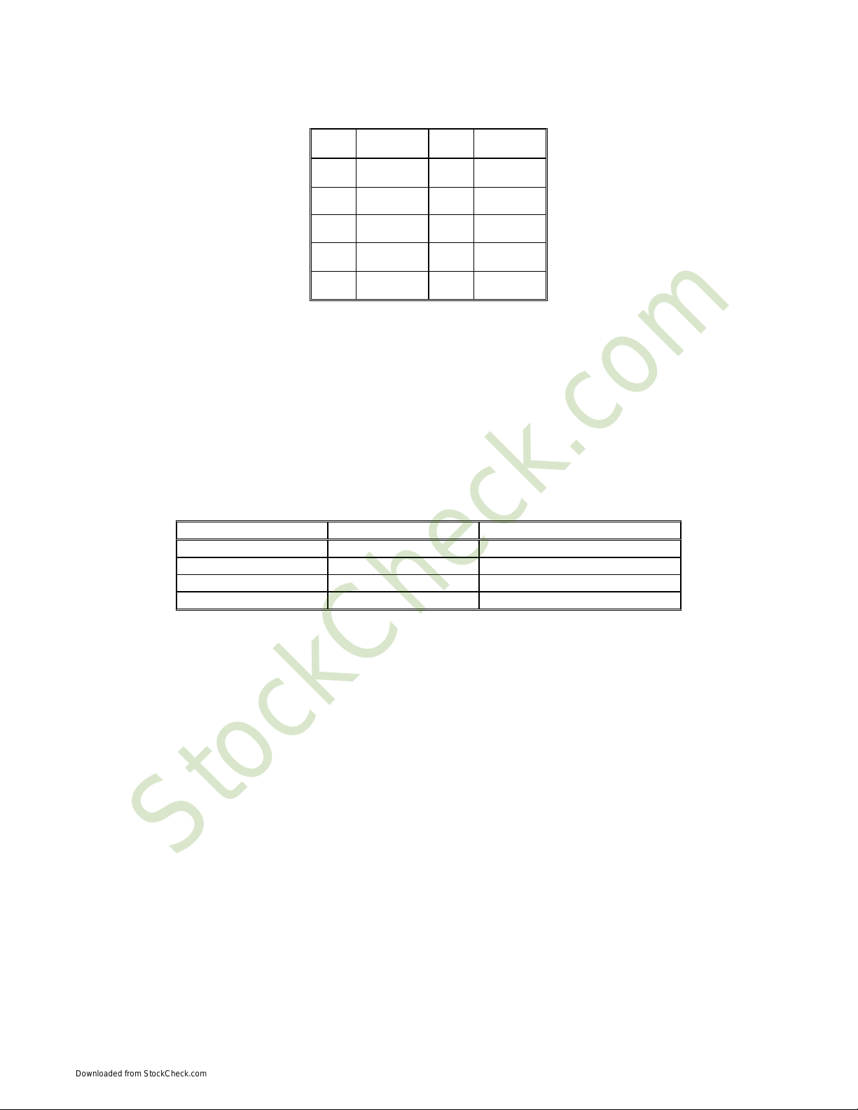
Register Map
The PC/104 programmer can access the IndustryPack modules on board the Flex/104A
using the set of registers listed below. These registers are located on the Flex/104A
card, not the IndustryPacks. Each register is at a unique offset address from the base
address. Base address for the Flex/104A is set using shunts E1 and E2. For more
information on the base address, refer to the Addressing section on page ?
Offset Register Name Read/Write
0x00 Data Register Read/Write
0x02 IP Access Register Write Only
0x04 Upper Address Register Write Only
0x06 Control and Status Read/Write
Figure 5 Register Map for the Flex/104A
StockCheck.com
Downloaded from StockCheck.com

7
Control & Status Register
15 14 13 12 11 10 9 8 7 6 5 4 3 2 1 0 Bit
0 0 0 0 0 0 0 0 0 IRQ1
B
IRQ1
A
IPWAI
T
TM
STAT
RST
STAT
IRQ0
B
IRQ0
A
Read
X X X X X X X X X X X X X X TM
RST
IP
RST
Write
0 0 0 0 0 0 1 0 0 IRQ1
B
IRQ1
A
0 0 0 IRQ0
B
IRQ0
A
Reset
6 IntReq1 B IRQ1 B R
This bit is set high when an IntReq1for IP slot B is asserted. It is cleared when the
interrupt is cleared. This bit is not latched on the Flex/104A.
5 IntReq1 A IRQ1 A R
This bit is set high when an IntReq1for IP slot A is asserted. It is cleared when the
interrupt is cleared. This bit is not latched on the Flex/104A.
4 IP Wait IP Wait R
This bit indicates whether or not an IP access is in progress. When this bit is one, an IP
access is in progress; otherwise, this bit is zero. Resets to zero.
3 Time Out Status TM Status R
This bit is asserted if an IP access has timed out. When an access is started, a timer
internal to the Flex/104A is enabled. If, after 64 µs, an acknowledge has not been
detected from the IP, the Flex/104A terminates the access and sets this bit high. To clear
this bit, a one must be written to bit 1 of the Control and Status Register. Resets to zero.
2 IP Reset Status RST STAT R
When this bit is asserted low, an IP reset is in progress; otherwise, this bit is high.
Resetting the IP bus requires approximately 250 ms.
1 Reset Time Out Status TM RST W
Writing a one to this bit resets the time out counter on board the Flex/104A.
1 IntReq0 B IRQ0 B R
This bit is set high when an IntReq0for IP slot B is asserted. It is cleared when the
interrupt is cleared. This bit is not latched on the Flex/104A.
0 IP Reset IP RST W
Writing a one to this bit generates an IP Reset* that lasts approximately 250 ms.
StockCheck.com
Downloaded from StockCheck.com

8
0 IntReq0 A IRQ0 A R
This bit is set high when an IntReq0for IP slot A is asserted. It is cleared when the
interrupt is cleared. This bit is not latched on the Flex/104A.
IP Access Register
15 14 13 12 11 10 9 8 7 6 5 4 3 2 1 0 Bit
X X X X X X X X X X X X X X X X Read
X X X X X X X SLOT IPSEL IP A6:1 Write
0 0 0 0 0 0 1 0 0 IRQ1
B
IRQ1
A
0 0 0 IRQ0
B
IRQ0
A
Reset
8 IP Slot Select SLOT W
This bit selects which IP slot is accessed. When this bit is zero, slot A is selected. When
one, slot B is selected.
7:6 IP Access Select IPSEL W
The IndustryPack bus provides for four address spaces: I/O, Memory, ID, and Interrupt.
These two bits determine what kind of access is made to the IP.
D7 D6 Access
Space
0 0 I/O Space
0 1 Memory
Space
1 0 ID Space
1 1 Interrupt
Space
Figure 6 IP Access Register Settings
5:0 IP Address Bit IP A6:1 R
These bits correspond to six dedicated address bits on the IP bus. When accessing an
IP, the value of the offset location for a given register on the IP must be programmed into
this field. Remember that the Flex/104A does not recognize the IP A0 bit and therefore
the value in the IP user manual must be shifted right by one bit.
Consider the following example for configuring the IP Access Register. Assume that an
IP is installed in slot A and that a register at offset 0x42 in Memory Space is to be
accessed. First, since the IP is in slot A, D8 must be set to zero. Next since the register
is located in memory space on the IP, bits D7 and D6 must be set to 01. Finally, the
offset of 0x42 must be shifted right by one bit. This yields a value of 0x21 or a binary
value of 100001. Putting all these bits together yields a value of 0x0061. This is the
value that must be written into the IP Access Register before accessing the Data
Register. Remember that the Flex/104A only recognizes 16-bit accesses.
StockCheck.com
Downloaded from StockCheck.com

9
Upper Address Memory
15 14 13 12 11 10 9 8 7 6 5 4 3 2 1 0 Bit
X X X X X X X X X X X X X X X X Read
IP A22:7 Write
0 0 0 0 0 0 0 0 0 0 0 0 0 0 0 0 Reset
When accessing an IP in memory space, the address bits A22 to A7 are required as well.
The Upper Address Register provides these bits to the IP bus. This register must be
programmed before accessing the data register.
Data Register
15 14 13 12 11 10 9 8 7 6 5 4 3 2 1 0 Bit
IP D15:0 Read
IP D15:0 Write
0 0 0 0 0 0 0 0 0 0 0 0 0 0 0 0 Reset
The Flex/104A is only capable of 16-bit addresses to the IndustryPack bus. The 16 bits
of read/write data are provided in the Data Register. The act of reading or writing the
Data Register begins the IP access. For this reason, you must first program the IP
Access Register and the Upper Address Register, if a memory access, before accessing
the data register.
StockCheck.com
Downloaded from StockCheck.com

10
Installing the IndustryPacks
IndustryPacks are installed on the Flex/104A carrier board by simply snapping them in.
Press the IP and the carrier board together with your fingers until the two pairs of mating
connectors are flush. The connectors are keyed, so the IP can only be installed correctly.
Proper anti-static handling procedures should be followed.
There are two locations for IPs. These are identified as Industry Pack A, Industry Pack B
After an IP has been installed, four stainless steel screws may be used to secure the IP
to the carrier board. This is normally necessary only in high vibration or shock
environments. Insert the screw through the IP and the two connectors. Attach the nut on
the solder side of the Flex/104A. Tighten using small tools, taking care not to damage
either the IP or the support board. The screws used are standard (metric) M2 x 18
stainless slotted flat head. The screws and nuts are supplied with each IP.
StockCheck.com
Downloaded from StockCheck.com

11
Specifications
Dimensions 4.55” x 4.55” with 0.50” x 0.325” cut outs near PC/104
connectors
Number of IndustryPacks Two single-wide, 1 double-wide
IP Clock Rate 8 MHz
I/O Interconnect Two 50-pin connectors
Power Requirements +5 VDC, TBD mA typ (Additional power is consumed by
IndustryPacks)
Environmental Operating temp: 0°to +70°C, -40°to +85°C (Flex/104-ET and
Flex/104A ET–
contact factory for availability)
Storage temp: -40°to +85°C
Humidity: 5% to 95% non-condensing
StockCheck.com
Downloaded from StockCheck.com
Table of contents
Other SBS Technologies Carrier Board manuals