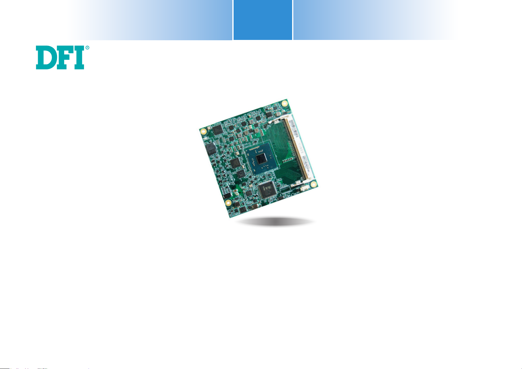
www.d.comChapter 2 Concept
9
Chapter 2
Specification Comparison Table
Module Pin-out - Required and Optional Features C-D Connector. PICMG®COM.0 Revision 2.1
The table below shows the COM Express standard specifications and the corresponding specifications supported on the BW968 module.
• 5 Indicates 12V-tolerant features on former VCC_12V signals.
• 6 Cells in the connected columns spanning rows provide a rough approximation of features
sharing connector pins.
PICMG®COM.0
COM Express®Module Base Specification
n 2.1 - Draft 0.92
3 Required and Optional Features
3.2 Module Pin-out Types 1-6 & 10 - Required and Optional Features
COM Express Required and Optional features are summarized in the following table. The features identified as Minimum (Min.) shall be i
Table 3.2: Module Pin-out - Required and Optional Features A-B Connector
Connector Feature
COM Express Module Base
Specification Type 6
(No IDE or PCI, add DDI+ USB3)
Min
Max
DFI BW968
Type 6
A-B
A-B PCI Express Lanes 0 - 5 1 / 6 3
A-B LVDS Channel A 0 / 1 0 / 1 (Option : eDP or LVDS)
A-B LVDS Channel B 0 / 1 1
A-B eDP on LVDS CH A pins 0 / 1 1 / 0 (Option : eDP or LVDS)
A-B VGA Port 0 / 1 0/1 (Option : DDI2 or VGA)
A-B TV-Out NA NA
A-B DDI 0 NA NA
A-B5Serial Ports 1 - 2 0 / 2 2
A-B CAN interface on SER1 0 / 1 0
A-B SATA / SAS Ports 1 / 4 2
A-B AC’97 / HDA Digital Interface 0 / 1 1
A-B USB 2.0 Ports 4 / 8 8
A-B USB Client 0 / 1 0
A-B USB 3.0 Ports NA NA
A-B LAN Port 0 1 / 1 1
A-B Express Card Support 1 / 2 2
A-B LPC Bus 1 / 1 1
A-B SPI 1 / 2 1
A-B
SDIO (muxed on GPIO) 0 / 1 0
General Purpose I/O 8 / 8 8
A-B SMBus 1 / 1 1
A-B I2C 1 / 1 1
A-B Watchdog Timer 0 / 1 1
A-B Speaker Out 1 / 1 1
A-B External BIOS ROM Support 0 / 2 1
A-B Reset Functions 1 / 1 1
5
Indicates 12V-tolerant features on former VCC_12V signals.
6
Cells in the connected columns spanning rows provide a rough approximation of features sharing connector pins.
Connector Feature
COM Express Module Base
Specification Type 6
(No IDE or PCI, add DDI+ USB3)
Min
Max
DFI BW968
Type 6
A-B
A-B Thermal Protection 0 / 1 1
A-B Battery Low Alarm 0 / 1 1
A-B Suspend/Wake Signals 0 / 3 1
A-B Power Button Support 1 / 1 1
A-B Power Good 1 / 1 1
A-B VCC_5V_SBY Contacts 4 / 4 4
A-B5Sleep Input 0 / 1 1
A-B5Lid Input 0 / 1 1
A-B5Fan Control Signals 0 / 2 2
A-B Trusted Platform Modules 0 / 1 1
A-B
A-B VCC_12V Contacts 12 / 12 12
Table 3.3: Module Pin-out - Re
tional Features C-D Connector
Connector Feature
COM Express Module Base
Specification Type 6
(No IDE or PCI, add DDI+ USB3)
Min
Max
DFI BW968
Type 6
C-D
PCI Express Lanes 16 - 31 0 / 16 0
PCI Express Graphics (PEG) 0 / 1 0
Muxed SDVO Channels 1 - 2 NA NA
PCI Express Lanes 6 - 15 0 / 2 0
PCI Bus - 32 Bit NA NA
PATA Port NA NA
LAN Ports 1 - 2 NA NA
DDIs 1 - 3 0 / 3 1/2
USB 3.0 Ports 0 / 4 2
C-D
C-D VCC_12V Contacts 12 / 12 12
Power
System I/O
Power
C-D6
C-D6
A-B6
System I/O
System Management
PICMG®COM.0
COM Express®Module Base Specification
n 2.1 - Draft 0.92
3 Required and Optional Features
3.2 Module Pin-out Types 1-6 & 10 - Required and Optional Features
COM Express Required and Optional features are summarized in the following table. The features identified as Minimum (Min.) shall be i
Table 3.2: Module Pin-out - Required and Optional Features A-B Connector
Connector Feature
COM Express Module Base
Specification Type 6
(No IDE or PCI, add DDI+ USB3)
Min
Max
DFI BW968
Type 6
A-B
A-B PCI Express Lanes 0 - 5 1 / 6 3
A-B LVDS Channel A 0 / 1 0 / 1 (Option : eDP or LVDS)
A-B LVDS Channel B 0 / 1 1
A-B eDP on LVDS CH A pins 0 / 1 1 / 0 (Option : eDP or LVDS)
A-B VGA Port 0 / 1 0/1 (Option : DDI2 or VGA)
A-B TV-Out NA NA
A-B DDI 0 NA NA
A-B5Serial Ports 1 - 2 0 / 2 2
A-B CAN interface on SER1 0 / 1 0
A-B SATA / SAS Ports 1 / 4 2
A-B AC’97 / HDA Digital Interface 0 / 1 1
A-B USB 2.0 Ports 4 / 8 8
A-B USB Client 0 / 1 0
A-B USB 3.0 Ports NA NA
A-B LAN Port 0 1 / 1 1
A-B Express Card Support 1 / 2 2
A-B LPC Bus 1 / 1 1
A-B SPI 1 / 2 1
A-B
SDIO (muxed on GPIO) 0 / 1 0
General Purpose I/O 8 / 8 8
A-B SMBus 1 / 1 1
A-B I2C 1 / 1 1
A-B Watchdog Timer 0 / 1 1
A-B Speaker Out 1 / 1 1
A-B External BIOS ROM Support 0 / 2 1
A-B Reset Functions 1 / 1 1
5
Indicates 12V-tolerant features on former VCC_12V signals.
6
Cells in the connected columns spanning rows provide a rough approximation of features sharing connector pins.
Connector Feature
Specification Type 6
(No IDE or PCI, add DDI+ USB3)
Min
Max
Type 6
A-B
A-B Thermal Protection 0 / 1 1
A-B Battery Low Alarm 0 / 1 1
A-B Suspend/Wake Signals 0 / 3 1
A-B Power Button Support 1 / 1 1
A-B Power Good 1 / 1 1
A-B VCC_5V_SBY Contacts 4 / 4 4
A-B5Sleep Input 0 / 1 1
A-B5Lid Input 0 / 1 1
A-B5Fan Control Signals 0 / 2 2
A-B Trusted Platform Modules 0 / 1 1
A-B
A-B VCC_12V Contacts 12 / 12
12
Table 3.3: Module Pin-out - Re
tional Features C-D Connector
Connector Feature
COM Express Module Base
Specification Type 6
(No IDE or PCI, add DDI+ USB3)
Min
Max
DFI BW968
Type 6
C-D
PCI Express Lanes 16 - 31 0 / 16 0
PCI Express Graphics (PEG) 0 / 1 0
Muxed SDVO Channels 1 - 2 NA NA
PCI Express Lanes 6 - 15 0 / 2 0
PCI Bus - 32 Bit NA NA
PATA Port NA NA
LAN Ports 1 - 2 NA NA
DDIs 1 - 3 0 / 3 1/2
USB 3.0 Ports 0 / 4 2
C-D
C-D VCC_12V Contacts 12 / 12 12
Power
System I/O
Power
C-D6
C-D6
A-B6
Change Key:
System I/O
System Management
Power Management
PICMG®COM.0
COM Express®Module Base Specification
n 2.1 - Draft 0.92
3 Required and Optional Features
3.2 Module Pin-out Types 1-6 & 10 - Required and Optional Features
COM Express Required and Optional features are summarized in the following table. The features identified as Minimum (Min.) shall be i
Table 3.2: Module Pin-out - Required and Optional Features A-B Connector
Connector Feature
COM Express Module Base
Specification Type 6
(No IDE or PCI, add DDI+ USB3)
Min
Max
DFI BW968
Type 6
A-B
A-B PCI Express Lanes 0 - 5 1 / 6 3
A-B LVDS Channel A 0 / 1 0 / 1 (Option : eDP or LVDS)
A-B LVDS Channel B 0 / 1 1
A-B eDP on LVDS CH A pins 0 / 1 1 / 0 (Option : eDP or LVDS)
A-B VGA Port 0 / 1 0/1 (Option : DDI2 or VGA)
A-B TV-Out NA NA
A-B DDI 0 NA NA
A-B5Serial Ports 1 - 2 0 / 2 2
A-B CAN interface on SER1 0 / 1 0
A-B SATA / SAS Ports 1 / 4 2
A-B AC’97 / HDA Digital Interface 0 / 1 1
A-B USB 2.0 Ports 4 / 8 8
A-B USB Client 0 / 1 0
A-B USB 3.0 Ports NA NA
A-B LAN Port 0 1 / 1 1
A-B Express Card Support 1 / 2 2
A-B LPC Bus 1 / 1 1
A-B SPI 1 / 2 1
A-B
SDIO (muxed on GPIO) 0 / 1 0
General Purpose I/O 8 / 8 8
A-B SMBus 1 / 1 1
A-B I2C 1 / 1 1
A-B Watchdog Timer 0 / 1 1
A-B Speaker Out 1 / 1 1
A-B External BIOS ROM Support 0 / 2 1
A-B Reset Functions 1 / 1 1
5
Indicates 12V-tolerant features on former VCC_12V signals.
6
Cells in the connected columns spanning rows provide a rough approximation of features sharing connector pins.
Connector Feature
COM Express Module Base
Specification Type 6
(No IDE or PCI, add DDI+ USB3)
Min
Max
DFI BW968
Type 6
A-B
A-B Thermal Protection 0 / 1 1
A-B Battery Low Alarm 0 / 1 1
A-B Suspend/Wake Signals 0 / 3 1
A-B Power Button Support 1 / 1 1
A-B Power Good 1 / 1 1
A-B VCC_5V_SBY Contacts 4 / 4 4
A-B5Sleep Input 0 / 1 1
A-B5Lid Input 0 / 1 1
A-B5Fan Control Signals 0 / 2 2
A-B Trusted Platform Modules 0 / 1 1
A-B
A-B VCC_12V Contacts 12 / 12 12
Table 3.3: Module Pin-out - Re
tional Features C-D Connector
Connector Feature
COM Express Module Base
Specification Type 6
(No IDE or PCI, add DDI+ USB3)
Min
Max
DFI BW968
Type 6
C-D
PCI Express Lanes 16 - 31 0 / 16 0
PCI Express Graphics (PEG) 0 / 1 0
Muxed SDVO Channels 1 - 2 NA NA
PCI Express Lanes 6 - 15 0 / 2 0
PCI Bus - 32 Bit NA NA
PATA Port NA NA
LAN Ports 1 - 2 NA NA
DDIs 1 - 3 0 / 3 1/2
O
tion : DDI2 or VGA
USB 3.0 Ports 0 / 4 2
C-D
C-D VCC_12V Contacts 12 / 12 12
System I/O
Power
C-D6
C-D6
A-B6
Change Key:
System I/O
System Management
Power Management