schroff maxpowerPRO CPA Series User manual

CPA Series OPERATING INSTRUCTIONS
AC/DCConverter compactPCI
13100 – 141 250 W
13100 – 145 500 W
•Fully compliant with PICMG 2.11 compactPCI
specification
•High density design in industry standard
3 U x 8 HP x 160 mm cassette 250 W
6 U x 8 HP x 160 mm cassette 500 W
•Input voltage range 90…264VAC with PFC
•4 high current outputs with flexible load
distribution
•Highly efficient topology with synchronous
rectifiers
•Included Or-ing FETs / Diode for true
redundant operation
•Remote sense, active current share for 3
outputs
•compactPCI compatible signalling
•Safety according IEC/EN 60950-1 and
UL 60950-1: cRUus / CE / TÜV
Selection Chart
Output 1 Output 2 Output 3 Output 4 Input Rated Type Schroff
Uo nom Io max Uo nom Io max Uo nom Io max Uo nom Io max Voltage Power part
[V DC] [A] [V DC] [A] [V DC] [A] [V DC] [A] Ui[V AC] Po nom [W] number
5.0 40 3.3 40 12 5.5 -12 2 90 - 264 250 CPA250 13100-141
5.0 50 3.3 60 12 12 -12 4 90 - 264 500 CPA500 13100-145
Purpose / Description
The maxpowerPRO Series are highly reliable power supplies for CompactPCI®systems, which are increasingly used in
communications, industrial, military, aerospace, and other applications. These power supplies offer high power density in plug-
in modules that meet the requirements of the PICMG®power interface specification for CompactPCI® systems.
The converters use the patented EDGETM technology and provide important advantages such as flexible output power,
extremely high efficiency, excellent reliability, full input-to-output isolation, negligible inrush current, hot-swap capability, soft
start, and overtemperature protection.
The inputs are protected against surges and transients occurring on the source lines and cover an operating input voltage
range from 90 to 264 VAC.
Important Note
Please read this operation instruction carefully before applying power. The warranty is subject to correct
input voltages being applied. Repairs or modifications made by anyone other than SCHROFF will
invalidate the warranty. This documentation has been complied with the utmost care. We cannot however
guarantee its correctness in every respect.
March 24, 2009 www.schroff.biz 73972-077/52 Page 1

OPERATING INSTRUCTIONS
Electrical Input Data
General Conditions: TA = 25 °C, unless TC is specified.
Input
CPA250
CPA500
Characteristics Conditions min typ max min typ max Unit
Vi Rated input voltage range Io= 0 – Io max 100 240 100 240
Vi op Operating input voltage TC min – TC max 90 264 90 264
Vi nom Nom. input voltage 50 – 60 Hz 1 230 230
Vi abs Input voltage limits without damage
280 0 280
VAC 1
Ii Typical input current Vi nom, Io nom 1.4 2.8
Ii max Max. input current Vi min, Io nom 3.6 4.0 7.1
Iinr p Peak inrush current Vi max, Io nom
15
20
A
Pi0 No-load input power Vi min –Vi max Io=
0 23 30 26 32 W
Pi inh Input power, when
inhibited Vi min – Vi max
3.2
3.2
Ci Input capacitance
1 4 µF
fswitch Switching frequency Vi nom, Io nom 135 135 kHz
th Hold-up time Vi min→0 V, Io nom
tbo Brown-out time Vi nom, Io nom 20
20
tsu Start-up time Vi nom, Io nom 150 150
ms
Power factor Vi nom, Io nom 0.95
0.95
W/VA
1 Rated input frequency: 50 – 60 Hz, operating input frequency range: 47 – 63 Hz
Short interruption of Viwithout affecting the outputs
Input Transient Protection
A metal oxide VDR (Voltage Dependent Resistor) together with the input fuse form an effective protection against high input
voltage transients, which typically occur in most installations.
Input Fuse
An incorporated miniature slow-blow fuse protects the converter
against further damage in the case of a failure.
Reverse polarity applied to the input of CPD models will cause the
fuse to blow but without other damage.
Model Fuse rating Reference
CPA250 250 VAC, 5 A T Schurter 0001.2511
CPA500 250 VAC, 10 A T Schurter 0034.6925
Note: The fuse is not customer-accessible.
Inrush Current Limitation
The converters incorporate an active inrush current limiter in the input circuitry, which reduces the peak inrush current value
by a factor of 10 – 15 to protect connectors and switching devices from damage.
Note: The inrush current limitation is achieved using electronic circuitry. For effective limitation the converter should not be
switched on and off more frequently than every 8 seconds.
Efficiency
The efficiency graph in the following figure shows the dependence
on input voltage (CPA models).
Page 2 www.schroff.biz

CPA Series OPERATING INSTRUCTIONS
March 24, 2009 www.schroff.biz 73972-077/52 Page 3
Electrical Output Data
General Conditions: CPA250: 400 LFM (2 m/s)
– TA= 25 °C, unless Tcis specified. – Sense lines connected directly at the connector
Output data of CPA250
Output Vo1 (5.0 V) Vo2 (3.3 V) Unit
Characteristics Conditions min typ max min typ max
Vo Output voltage Vi nom, 50% Io nom 4.95 5.0 5.05 3.267 3.3 3.333 VDC
Io
nom Nominal output current 25 20
Io
max Max. output current Vi min –Vi max 40 40
IoL Output current limit TC min – TC max 50 50
Io
min Minimum load no min. load required no min. load required
A
vo Switch.
frequ. Vi nom, Io nom BW = 20 MHz
25 20
Output
voltage
noise Total Cext = 22 µF + 100 nF 60 60
mVpp
∆Vo
V Static line regulation Vi min –Vi max, Io nom ±10 ±10
∆Vo
L Static load regulation Vi nom, 50 – 100% Io max ±10 ±10
∆Vo
S
Overshoot at switch
on/off 0 0
mV
vo d Dynamic
load
Voltage
deviation
Vo1: ∆Io1 = 10 A, dIo1/dt = 2 A/µs
Vo2: ∆Io2 = 10 A, dIo2/dt = 2 A/µs
± 120
± 120 mV
td regulatio
n
Recovery
time 100 100 µs
αVo Temperature coefficient
of output voltage TC min –TC max 0–Io nom, Vi min –Vi
max
±0.3 ±0.2 mV/K
Output Vo3 (+12 V) Vo4 (–12 V) Unit
Characteristics Conditions min typ max min typ max
Vo Output voltage Vi nom, 50% Io nom 11.88 12.0 12.12 –11.52 –12.0 –12.48 VDC
Io nom Nominal output current
4
1A
Io max Max. output current Vi min –Vi max 5.5
2
IoL Output current limit TC min – TC max
7
3.5
Io min Minimum load Io3 > 75% Io4 1
vo Switch.
frequ. Vi nom, Io nom BW = 20 MHz
mVpp
Output
voltage
noise Total Cext = 22 µF + 100 nF 120 120
∆VoV Static line regulation Vi min –Vi max, Io nom ±10 ±10 mV
∆VoL Static load regulation Vi nom, Io = 1 – 2 A ±30 – 380 2
∆VoS Overshoot at switch
on/off 0 0
Vo3: ∆Io3 = 2 A, dIo3/dt = 2 A/µs ± 200 ± 200
vo d
Voltage
deviation Vo4: ∆Io4 = 0.5 A, dIo4/dt = 2
A/µs
td
Dynamic
load
regulation Recovery
time 500 500 µs
αVo
Temperature
coefficient
of output voltage
TC min –TC max
0–Io nom,Vi min –Vi max ±0.3 ±0.5 mV/K
1Minimum load is only required to maintain regulation of Vo4
2Droop characteristic for passive current sharing

OPERATING INSTRUCTIONS
Page 4 www.schroff.biz
General Conditions:
• TA= 25 °C, unless Tcis specified.
• CPA500: 300 LFM (1.5 m/s)
• Sense lines connected directly at the connector
Output data of CPA500
Output Vo1 (5.0 V) Vo2 (3.3 V) Unit
Characteristics Conditions min typ max min typ max
Vo Output voltage Vi nom, 50% Io nom 4.95 5.0 5.05 3.267 3.3 3.333 VDC
Io
nom Nominal output current 40 50
Io
max Max. output current Vi min –Vi max 50 60
IoL Output current limit TC min – TC max 52,2 62 63 74
Io
min Minimum load no min. load required no min. load required
A
vo Switch.
frequ. Vi nom, Io nom BW = 20 MHz
20 15
Output
voltage
noise Total Cext = 22 µF + 100 nF 20 15
mVpp
∆Vo
V Static line regulation Vi min –Vi max, Io nom ±10 ±10
∆Vo
L Static load regulation Vi nom, 50 – 100% Io max ±10 ±10
∆Vo
S
Overshoot at switch
on/off 0 0
mV
vo d Dynamic
load
Voltage
deviation
Vo1: ∆Io1 = 10 A, dIo1/dt = 2 A/µs
Vo2: ∆Io2 = 10 A, dIo2/dt = 2 A/µs
± 150
± 150 mV
td regulation Recovery
time 300 300 µs
αVo Temperature coefficient
of output voltage TC min –TC max 0–Io nom, Vi min –Vi
max
±0.3 ±0.2 mV/K
Output Vo3 (+12 V) Vo4 (–12 V) Unit
Characteristics Conditions min typ max min typ max
Vo Output voltage Vi nom, 50% Io nom 11.88 12.0 12.12 –11.52 –12.0 –12.48 VDC
Io nom Nominal output current
8
3A
Io max Max. output current Vi min –Vi max 12
4
IoL Output current limit TC min – TC max 13,5 4,3
Io min Minimum load Io3 > 75% Io41
vo Switch.
frequ. Vi nom, Io nom BW = 20 MHz
mVpp
Output
voltage
noise Total Cext = 22 µF + 100 nF 15 10
∆VoV Static line regulation Vi min –Vi max, Io nom ±10 ±10 mV
∆VoL Static load regulation Vi nom, Io = 1 – 2 A ±50 – 220 2
∆VoS Overshoot at switch
on/off 0 0
Vo3: ∆Io3 = 2 A, dIo3/dt = 2 A/µs ± 200 ± 150
vo d
Voltage
deviation Vo4: ∆Io4 = 0.5 A, dIo4/dt = 2
A/µs
td
Dynamic
load
regulation Recovery
time 300 300 µs
αVo
Temperature
coefficient
of output voltage
TC min –TC max
0–Io nom,Vi min –Vi max ±0.3 ±0.5 mV/K
1Minimum load is only required to maintain regulation of Vo4
2Droop characteristic for passive current sharing

CPA Series OPERATING INSTRUCTIONS
Hot Swap
Hot swap is possible. The output voltages may deviate dynamically by ≤5% during the plug-in / plug-out operation.
Output Characteristic and Protection
All outputs are fully protected against continuous opencircuit
(no load) and continuous short-circuit conditions.
All outputs of CPA250 models have a constant current
limitation with a rectangular characteristic. In addition, the total
power from outputs Vo1, Vo2, and Vo3 is limited to Po max,
resulting in a free choice of load distribution between these
outputs. Output Vo4 is disabled in the case of overtemperature
generated by overcurrent.
In CPA500 model, the total power of all four outputs is limited
to Po max.
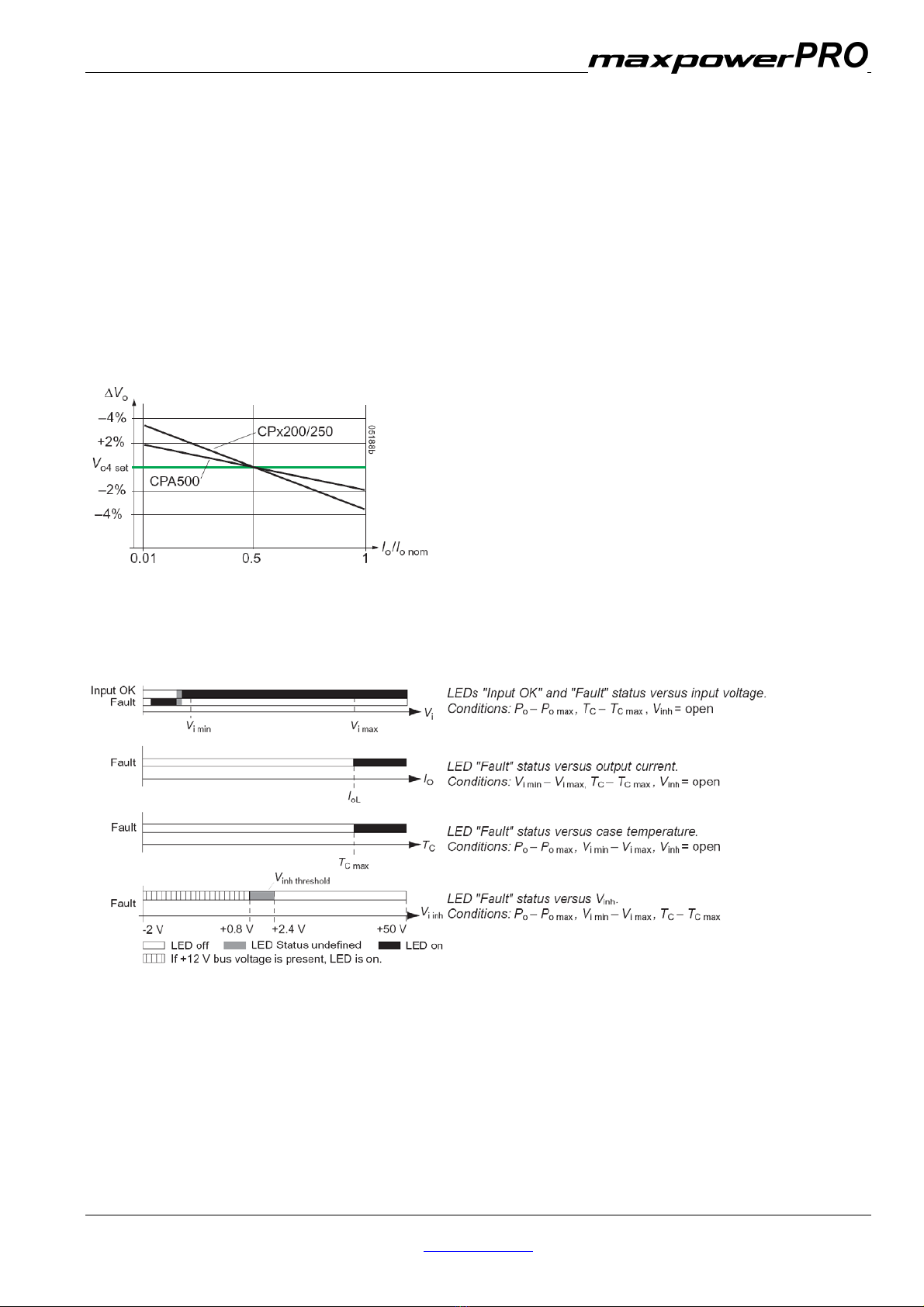
In all models, all outputs are monitored for overvoltage
condition. If an overvoltage of 120 – 130% is dedected, the
converter is permanently disabled. To reset, the input voltage
must be removed for 60 seconds.
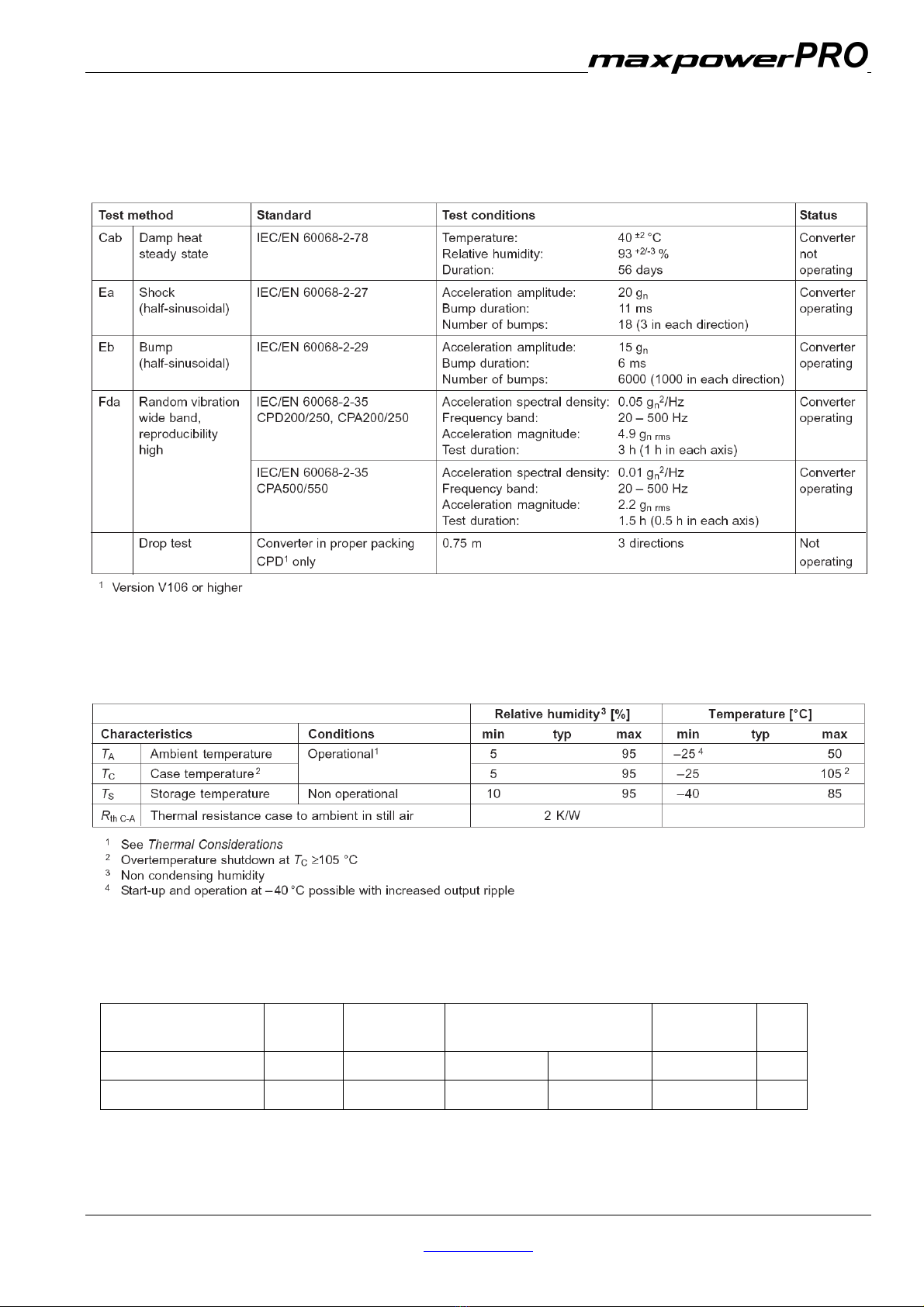
Thermal Considerations
If a converter is mounted in the upright position with
airflow as specified in the general conditions allowing
unrestricted forced-air cooling, and is operated at its
nominal input voltage and power at maximum ambient
temperature TA max (see Temperatures), the
temperature measured at the measurement point of the
case temperature TC (see Mechanical Data) will
approach after an initial warm-up phase the indicated
maximum value of TC max (105 °C). However, the
relationship between TA and TC depends heavily on the
operating conditions and system integration. The thermal
conditions are significantly influenced by the input
voltage, the output current, the airflow, and the
temperature of the adjacent elements and surfaces. TA
max is therefore only an indicative value (contrary to TC
max).
Caution: The installer must ensure that under all operating
conditions TCremains within the limits shown in the diagrams of
fig. 4.
Output power versus temperature TAat Vi nom (CPD/CPA250)
Note: Forced-air cooling or an additional heat sink can improve
the reliability or allow TAto be increased above TA max, provided
that TC max is not exceeded.
Thermal Protection
A temperature sensor fitted on the main PCB provides an
overtemperature warning (degrade) signal 15 °C below
the temperature Tc max, at which the thermal derating
begins to reduce the output power. The output power
returns to the normal value, when the temperature drops
back below this limit; see Temperature Warning and
Shutdown.
Output power versus temperature TAat Vi nom
(CPA500/550)
March 24, 2009 www.schroff.biz 73972-077/52 Page 5

OPERATING INSTRUCTIONS
Output Filter
The output ripple voltage can be reduced by an external filter to less then 5 mVpp. Recommended values:
• C1, C2: Low ESR capacitor, e.g., OS-CON 100 – 470 µF
• L1, L2: Choke 1 – 2.2 µH with appropriate rated current, e.g., Coiltronics®HC2LP 1 µH /33 A or 2.2 µH /24 A.
Output filter reducing the output ripple of Vo1 and Vo2
Auxiliary Functions Inhibit and Enable
The inhibit input enables (logic high) or disables (logic low, pull down) all outputs, if a logic signal (TTL, CMOS) is applied. In
systems consisting of several converters this feature may be used to control the activation sequence of the converters by
means of logic signals, or to enable the source to start-up, before full load is applied.
Note: If this function is not used, the inhibit pin 39 can be left open-circuit (not connected). If pin 39 is connected to a return pin (e.g., pin 22),
the internal logic will disable all outputs. The inhibit input is protected by a decoupling diode.
Characteristics Conditions min typ max Unit
Vo= off –20.8 V
Vinh inhibit
voltage Vo= on Vi min –Vi max
Io = 0 – Io max 2.4 50
trRise time
120 ms
tfFall time depending on Io
Inhibit and enable inputs
Typical output response as a function of inhibit voltage
The enable pin 27 (EN#) must be connected to a return pin (e.g., pin 22) enable the converter. Pin 27 is shorter than the
others ensuring startup only, when all other pins are already connected to the system providing true hot-swap capability.
Page 6 www.schroff.biz

CPA Series OPERATING INSTRUCTIONS
Temperature Warning and Shutdown
A temperature warning circuitry monitors the case temperature TC. Its output signal VDEG#changes from high to low
impedance, when the TCexceeds the upper threshold level, and changes back to high impedance, when TCfalls below the
lower threshold level, which is 85 °C ± 5 °C.
Pin 38 (degrade signal DEG#) is internally connected via the collector-emitter path of an NPN transistor to the signal return pin
22. The current IDEG# through pin 38 should not exceed 40 mA, and VDEG# should not exceed 40 V.
If TC exceeds 105 °C, the converter will be disabled. It resumes operation automatically, once TC falls below 105 °C.
Degrade signal: NPN output VDEG# ≤40 V, IDEG# ≤20 mA Degrade signal VDEG# versus case temperature TC
Power Fail Signal
The power fail circuitry monitors the input voltage and all output
voltages. Its output signal VFAL# changes from high to low impedance
(<0.5 V), when one of the monitored voltages falls below the threshold
level; VFAL# changes back to high impedance, when all monitored
voltages exceed their threshold level.
The threshold levels correspond to approx. 85% of Vo nom. Vi min CPA250
up to Version V115 is not monitored. Vi min of CPA models is considered
as insufficient, when vi remains for typ. 30 ms below √
–
2 • Vi min.
Connector pin 42 (signal VFAL#) is internally connected via the drain-
source path of a JFET (self-conducting type) to the signal return pin 22.
The current IFAL# should not exceed 10 mA. VFAL# should not exceed 40
V, as the JFET is not protected against overvoltage. Power Fail: JFET output, IFAL# ≤10 mA
Sense Lines
(Only for Vo1, Vo2, and Vo3.)
This feature allows the compensation of voltage drops across the connector contacts and if necessary, across the load lines.
To ensure correct operation, all sense lines S+ (Vo1SENSE Vo2SENSE, and Vo3SENSE) should be connected to the
respective power outputs. The common sense return S– (SRTN) should be connected to RTN (pin 5 – 12).
Note: Open sense lines are admissible, but the output voltage regulation will be poor.
The voltage difference between any sense line at its respective power output pin (as measured on the connector) should not
exceed the following values.
Output
[V] Total voltage difference between sense lines
and their respective outputs
3.3 0.8 V
5 1 V
12 1 V
Sense line data
Note: If the sense lines S+ and S– compensate for a considerable voltage drop, the output loads shall be reduced in order to respect the
maximum output power.
March 24, 2009 www.schroff.biz 73972-077/52 Page 7

OPERATING INSTRUCTIONS
Active Current Sharing for Vo1, Vo2, Vo3
The current sharing facility, consisting of a single-wire link, should be used, where several converters are operated in parallel
connection, for example, high reliability n+1 redundant systems or systems providing higher output power.
Note: Not more than six converters should be connected in parallel.
Using this feature reduces the stress of the individual converters and improves the reliablity of the system. Interconnection of
the current sharing terminals causes the converters to share the output current evenly. In n+1 redundant systems a failure of a
single converter will not lead to a system failure, since the outputs are already decoupled by FETs and diodes internally.
Passive Current Sharing for Vo4
The output voltage changes slightly with the output current (droop characteristic) ensuring automatic current sharing without
further precautions, when several converters are connected in parallel. An increase in output current decreases the output
voltage according to the following graph. ∆Vo –4% +2%
Output voltage Vo4 versus output current Io4.
LEDs
A green LED "Input OK" and a red LED "Fault" are incorporated in the front panel.
Page 8 www.schroff.biz

CPA Series OPERATING INSTRUCTIONS
Electromagnetic Compatibility (EMC)
A metal oxide VDR together with an input fuse and filter form an effective protection against high input voltage transients,
which typically occur in most installations. The converters have been successfully tested to the following specifications
Electromagnetic Immunity
Immunity type tests
Electromagnetic Emission
Radiated and conducted emissions comply with EN 55011/ 55022, class A. In addition, CPA500/550 meet conducted
emissions class B.
Typical disturbance voltage (peak) at the line input
according to EN 55022, measured at Vi nom and Io nom
CPA500
Typical disturbance voltage (peak) at the line input
according to EN 55022, measured at Vi nom and Io nom
CPA250
March 24, 2009 www.schroff.biz 73972-077/52 Page 9

OPERATING INSTRUCTIONS
Immunity to Environmental Conditions
Mechanical and climatic stress
Temperatures
Temperature specifications, valid for an air pressure of 800 – 1200 hPa (800 – 1200 mbar)
Reliability
MTBF
Ratings at specified
case temperature Model Ground
benign 40 °C Ground fixed 40 °C 70 °C Ground
mobile 50 °C Unit
MTBF acc. to CPA250 279 000 57 000 31 000 33 000 h
MIL-HDBK-217F, notice 2 CPA500 195 000 35 000 17 000 16 000 h
Page 10 www.schroff.biz

CPA Series OPERATING INSTRUCTIONS
Mechanical Data Pin allocation
Connector: Positronic (PCIH47M400A1)
Pin12Signal
Name Description
1-4 M V1 V1 Output
5-12 M RTN V1 and V2 Return
13-18 M V2 V2 Output
19 M RTN V3 Return
20 M V3 V3 Output
21 M V4 V4 Output
22 M RTN Signal Return
23 M Reserved Reserved
24 M RTN V4 Return
25 M Reserved 3
26 M Reserved Reserved
27 S EN# Enable
28 M Reserved 3
29 M nc Not connected
30 M V1SENSE V1 Remote Sense
31 M Reserved 3
32 M nc Not connected
33 M V2SENSE V2 Remote Sense
34 M S RTN Sense Return
35 M V1SHARE V1 Current Share
36 M V3SENSE V3 Remote Sense
37 M Reserved 3
38 M DEG# Degrade Signal
39 M INH# Inhibit
40 M Reserved 3
41 M V2SHARE V2 Current Share
42 M FAL# Fail Signal
43 M Reserved 3
44 M V3SHARE V3 Current Share
45 L CGND Chassis Ground
46 M ACN AC Input Neutral
47 M ACL AC Input Line
Dimensions in mm.
1Pin number illustrated are of the female backplane connector
2L=first mate, M=second mate, S=last mate
3For future options
Overall size: 162.5 mm x 128.7 mm x 40.6 mm Weight: 0.8 kg
Overall size: 223.4 mm x 162.5 mm x 40.6 mm Weight: 1.65 kg
March 24, 2009 www.schroff.biz 73972-077/52 Page 11

OPERATING INSTRUCTIONS
Page 12 www.schroff.biz
Accessories (optional)
Mating connector / intermediate plate 3 U for one PSU Order No.: 23098 – 105
Mating connector / intermediate plate 3 U for two PSUs horizontally Order No.: 23098 – 115
Mating connector / intermediate plate 6 U for one PSU Order No.: 23098 – 116
Mating connector / intermediate plate 6 U for two PSUs vertical Order No.: 23098 – 117
Caution & Notes
CAUTION
These component level power supplies are intended exclusively for installation within other equipment
by an industrial assembly operation or by professional installers. These are Class I power supplies; the
ground pin of input connector J1 must be properly connected to earth ground in end use. Component
power supplies are to be installed in end-use equipment according to the requirements of the safety
standard used for that equipment. These power supplies are not designed to be operated outside of an
enclosure which provides a means of mechanical, electrical, and fire protection. To maintain SELV
requirements, the outputs should not be connected together in any manner which causes the total
output voltage to exceed 60 VDC.
PROTECTIVE EARTHING
The Power Supply must be properly grounded to mains protective earthing termination at end use.
FUSING
In case of failure, the Power Supply must be returned to a Schroff Authorized Service Center. There
are no user-serviceable parts in the Power Supply.
LIMITED WARRANTY
Schroff warrants each power supply of its manufacture for a period of two (2) years from the date of
original shipment. This warranty applies to defects in materials and workmanship that result in non-
performance to published specifications.
Schroff assumes no liabilities for consequential damages of any kind through the use or misuse of its
products by any user. No other obligations are expressed or implied.
Please note that the specifications, terms, and conditions stated are subject to change without notice.
SCHROFF GmbH
Langenalber Strasse 96 – 100
D – 75334 Straubenhardt
Phone: +49 7082 794 – 0
Fax: +49 7082 794 – 200 Web: www.schroff.biz
Table of contents
Popular Media Converter manuals by other brands

Decimator
Decimator MD-HX operating manual

Frauscher Sensortechnik GmbH
Frauscher Sensortechnik GmbH WSC001 Technical documentation

Edision
Edision Home Modulator user manual

Stoltzen
Stoltzen APOLLO SA-6000E user manual

urmet domus
urmet domus iPer VOICE 1039 manual

Marklin Digital
Marklin Digital 60842 manual