Seiko Epson RTC-4553AC Instructions for use


NOTICE
• No part of this material may be reproduced or duplicated in any form or any means without the written
permission of Seiko Epson.
• Seiko Epson reserves the right to make changes to this material without notice.
• Seiko Epson does not assume any liability of any kind arising out of any inaccuracies contained in this
material or due to its application or use in any product or circuit and, further, there is no representation
that this material is applicable to products requiring high level reliability, such as, medical products.
• Moreover, no license to any intellectual property rights is granted by implication or otherwise, and there
is no representation or warranty that anything made in accordance with this material will be free from
any patent or copyright infringement of a third party.
• This material of portions thereof may contain technology or the subject relating to strategic products
under the control of the Foreign Exchange and Foreign Trade Law of Japan and may require an export
license from the Ministry of international Trade and industry or other approval from another government
agency.
In pursuit of "Saving" Technology ,Epson electronic device.
Our Lineup of semiconductors, Liquid crystal displays and quartz devices
assists in creating the products of our customers' dreams.
Epson IS energy savings.
Downloaded from Elcodis.com electronic components distributor

RTC – 4553AC
CONTETS
1. Overview..........................................................................................1
2. Block Diagram.................................................................................1
3. Terminal description ........................................................................2
3.1. Terminal connections........................................................................................ 2
3.2. Terminal functions............................................................................................. 2
4. Absolute maximum ratings...............................................................3
5. Recommended operating conditions................................................3
6. Frequency characteristics................................................................3
7. Electrical characteristics..................................................................4
7.1. DC, AC Characteristics..................................................................................... 4
7.1.1. VDD = 5 V...........................................................................................................................4
7.1.2. VDD = 3 V...........................................................................................................................5
7.2. Timing Chart..................................................................................................... 6
8. How to use.......................................................................................7
8.1. Registers........................................................................................................... 7
8.1.1. Register Table................................................................................................................... 7
8.1.2. Register Bit Functions ....................................................................................................... 8
8.2. Register Description.......................................................................................... 9
8.2.1. Time/Calendar Counter Registers.....................................................................................9
8.2.2. Control Registers............................................................................................................. 10
8.3. How to use...................................................................................................... 12
8.3.1. Data Read ....................................................................................................................... 12
8.3.2. Data Write/Modify............................................................................................................ 12
8.3.3. Initialize............................................................................................................................ 12
8.3.4. Timing Pulse Output........................................................................................................ 12
8.3.5. Sample Operation Flow Charts........................................................................................13
8.3.6. CS1 and CS0 Operation................................................................................................. 15
8.3.7. System Power Down During Interface Operation............................................................ 15
8.3.8. Power Supply and CS1 Operation................................................................................... 15
8.3.9. Power-On Reset.............................................................................................................. 16
8.3.10. Power Supply Connection Example ..............................................................................16
8.3.11. Processing of Non-Existent Data...................................................................................17
8.3.12. Timing Charts................................................................................................................ 18
9. External dimensions / Marking layout ............................................21
9.1. External dimensions........................................................................................ 21
9.2. Marking layout................................................................................................. 21
10. Reference Data ...........................................................................22
11. Application notes .........................................................................23
11.1. Notes on handling......................................................................................... 23
11.2. Notes on packaging...................................................................................... 23
Downloaded from Elcodis.com electronic components distributor
RTC – 4553AC
Page - 1 MQ - 342 - 01
Real-Time Clock Module
RTC – 4553AC
•Designed for E-mater
•Built-in 32.768 kHz quartz crystal allows adjustment- free operation and assures high accuracy
•Integrated clock (hours, minutes, seconds) and calendar (year, month, day, day of the week) counter
•Automatic leap year compensation until 2099
•Selectable 24-hour/12-hour display mode (with AM/PM indication)
•Clock data modification using increment method
•Clock data serial output in BCD format
•Software controlled 30 second adjustment
•Selectable 1/10 Hz or 1024 Hz timing pulse output
•Built-in SRAM (30 ×4 bit)
•Constant voltage drive realizes low power consumption (1 µA Typ.)
and minimizes voltage-induced frequency fluctuations
•Supports low-voltage operation (3 V)
1. Overview
The RTC-4553 is a very compact real-time clock module with permanent calendar and serial data
input/output. The module is designed for E-mater; time accuracy is within ±5×10⁻⁶ (±0.432 sec./day).
It incorporates a heat-resistant 32.768 kHz quartz oscillator. The space saving package allows high-density
mounting and facilitates automated production.
Besides the clock and calendar functions (comprising all items from years to seconds), the RTC-4553
incorporates also a 30 ×4 bit SRAM and offers other useful features.
The use of a CMOS IC makes possible low-voltage, low-power operation, to ensure proper timekeeping
also when powered from a backup battery.
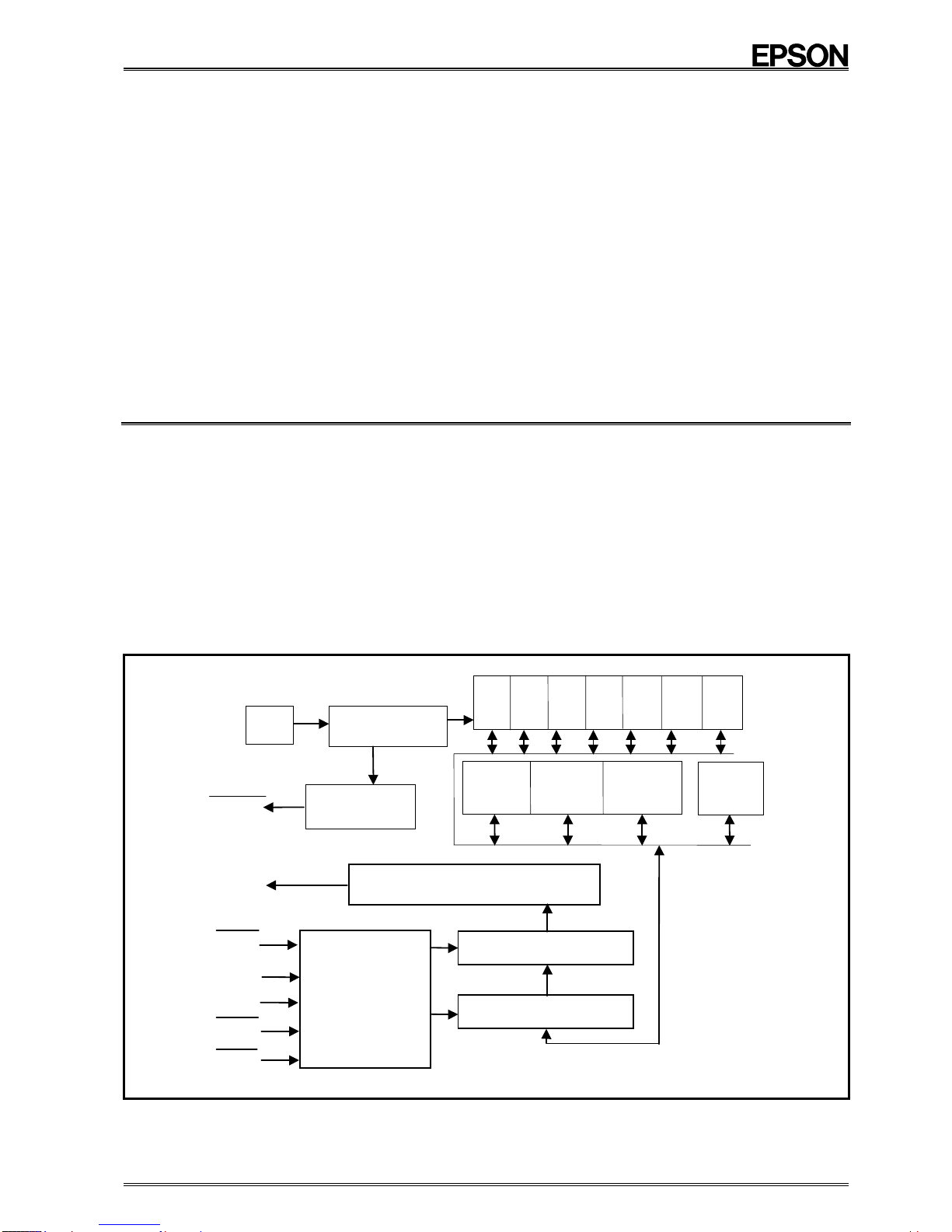
2. Block Diagram
YearMon.Day
Hou. Day
of
week
Min.
Control circuit
Shift controller
Input
controller
Output controller
Control
register
3RAM
(120bit)
Control
register
2
Control
register
1
Output
controller
32.768 kHz
OSC Counter Sec.
TPOUT
WR
CS0
CS1
SCK
SIN
SOUT
Downloaded from Elcodis.com electronic components distributor

RTC – 4553AC
Page - 2 MQ - 342 - 01
3. Terminal description
3.1. Terminal connections
RTC - 4553
1. GND 14. TPOUT
2. WR 13. SOUT
3. SIN 12. CS1
4. SCK 11. CS0
5. L110. L5
6. L29. L4
7. L3
# 1
# 7
#14
# 8 8. VDD
SOP - 14 pin
3.2. Terminal functions
Signal designation Pin No. Input
/ Output Function
GND 1 — Power supply negative pin. Connect to ground.
WR
( WRITE enable ) 2 I
Address and data are written at WR = "L". Counter data (second digit to
year digit) are written using the incrementing method.
Data at the specified address are read at WR = "H". While the address is
being set at SIN, the data at SOUT are for the previously specified address.
SIN
( Serial input ) 3 I
Serial address and data I/O pin. Serves for address and control register
writing for the various counters, and for RAM address and data writing.
SCK
( Serial clock ) 4 I
Serial I/O sync signal input pin. Input a sync signal to this pin to allow address
and data read/write synchronized to this signal.
One cycle comprises 8 clocks (4 address clocks + 4 data clocks)
L1−L3
L4 , L5 5−7
9, 10 — Test pins reserved for use by Epson. Be sure to leave these pins
unconnected.
VDD 8 —
Power supply pin. Connect to a power source. For normal operation and bus
access, supply 5 V ±10% or 3 V ±10%. For backup battery operation, provide
a voltage of 2 V or higher.
See Note 1.
CS0
( Chip select 0 ) 11 I
This pin serves to select the RTC. While CS0 is "L", the microprocessor
can perform register access. While CS0 is "H", SOUT is in the
high-impedance state.
CS1
( Chip select 1 ) 12 I
Connect this pin to the power down detection circuit. If no power down
detection circuit is used, fix the pin at "H" (VDD). When CS1 is "L", SOUT and
TPOUT are in the high-impedance state, regardless of CS0 .
SOUT
( Serial output ) 13 O
Serial address and data output pin. Serves for address and control register
readout of the various counters, and for RAM address and data readout.
TPOUT
( Timing pulse
output ) 14 O
Output pin for 1024 Hz or 1/10 Hz timing pulse, based on internal reference
clock. For clock accuracy checking, use 1/10 Hz.
For 1024 Hz, the duty cycle changes once every 10 seconds.
Note1 At initial power-on or voltage restoration from an intermediate potential outside of the range where operation is
assured (0.3 V to 1.9 V), the power-on reset circuit may not operate normally, leading to possible malfunction.
(See section " 8.3.9. Power-On Reset ".)
Note2 Be sure to connect a bypass capacitor of 0.1 µF or more directly between VDD and GND.
Downloaded from Elcodis.com electronic components distributor

RTC – 4553AC
Page - 3 MQ - 342 - 01
4. Absolute maximum ratings GND=0 V
Item Symbol Condition (pin) Min. Max. Unit
Power supply voltage VDD VDD−GND −0.3 +6.0
Input voltage VIN S
IN, SCK , WR , CS0 , CS1 −0.3 VDD+0.3
Output voltage VOUT S
OUT, TPOUT −0.3 VDD+0.3
V
Storage temperature TSTG Stored bare product after unpacking −55 +125 °C
Soldering conditions TSOL —
Twice at under +260 °C within 10 seconds, or
under +230 °C within 3 minutes
5. Recommended operating conditions GND=0 V
Item Symbol Condition Min. Typ. Max. Unit
Power supply voltage VDD VDD−GND 2.7 5.0 5.5 V
Operation temperature TOPR No condensation −30 — +70 °C
6. Frequency characteristics GND=0 V
Item Symbol Condition Rating Unit
± 5 ×10⁻⁶
Frequency precision ∆f / fo Ta = +25 °C
VDD = 5.0 V AC ± 0.432 sec. / day
Frequency/temperature
characteristics tOP Ta = −10 °C to +70 °C,
VDD = 5 V (Referenced at +25 °C ) +10
−120 ×10-6
Frequency/voltage
characteristics f / V Ta = Fixed, VDD = 2 V to 5.5 V
(Referenced at 5 V) ± 5 ×10⁻⁶
Aging fa Ta = +25 °C, VDD = 5 V, First year ± 5 ×10⁻⁶ / year
Note
(1) Frequency tolerance rating applies to VDD = 5.0 V.
(AtV
DD = 3 V, voltage characteristics must be taken into consideration.)
(2) Frequency tolerance rating applies at the time of shipment.
(3) Design the peripheral circuitry so that power start-up time (tR) is 1.0 µs/V ≤tR≤1.6 ms/V.
Downloaded from Elcodis.com electronic components distributor

RTC – 4553AC
Page - 4 MQ - 342 - 01
7. Electrical characteristics
7.1. DC, AC Characteristics
7.1.1. VDD = 5 V
(1) DC Characteristics ( GND=0 V , Ta = −30 °C ∼+70 °C )
VDD = 5 V ± 10 %
Item Symbol Condition Min. Typ. Max. Unit
Data retention
voltage VDH — 2.0 — 5.5 V
IDD1
(normal operation) SCK = 500 kHz
CS0 = L, CS1 = H — — 100
Current
consumption IDD2
(backup
operation)
SCK = 0 Hz
CS0 = H, CS1 = L — 1.0 3.0
µA
VOH IOH = −400 µA VDD −
0.4 — —
Output voltage VOL I
OL = 1.6 mA — — 0.4 V
IOZH V
OUT = 5.5 V −2.0 — 2.0
Output leak
current IOZL V
OUT = 0 V −2.0 — 2.0 µA
VIH — 4/5 VDD — —
Input voltage VIL — — — 1/5 VDD V
IIH V
IN = 5.5 V −2.0 — 2.0
Input current IIL V
IN = 0 V −2.0 — 2.0 µA
Oscillation
startup time Ts Ta = +25 °C — — 3.0 s
(2) AC Characteristics ( GND=0 V , Ta = −30 °C ∼+70 °C )
VDD = 5 V ± 10 %
Item Symbol Condition Min. Typ. Max. Unit
SCK frequency fCLK — — — 500 kHz
SCK "L" time tWCKL — 1.0 — —
SCK "H" time tWCKH — 1.0 — —
SCK pause time tPS — 1.0 — —
CS0 setup time tSCS — 0 — —
CS0 hold time tHCS — 0.5 — —
SIN data setup time tSD — 0.2 — —
SIN data hold time tHD — 0.2 — —
WR setup time tSWR — 1.0 — —
WR hold time tHWR — 0.5 — —
µs
SOUT delay time tDS0 CL=100 pF — 150 500
Time lag between CS0 , CS1 enable
and SOUT output tDSZ1 CL=100 pF — — 100
Time lag between CS0 disable and
SOUT high Z tDSZ2 CL=100 pF — — 100
Time lag between CS1 enable and
TPOUT output tDPZ1 CL=100 pF — — 100
Time lag between CS1 disable and
TPOUT high Z tDPZ2 CL=100 pF — — 100
ns
Downloaded from Elcodis.com electronic components distributor

RTC – 4553AC
Page - 5 MQ - 342 - 01
7.1.2. VDD = 3 V
(1) DC Characteristics ( GND=0 V , Ta = −30 °C ∼+70 °C )
VDD = 3 V ±10 %
Item Symbol Condition Min. Typ. Max. Unit
Data retention
voltage VDH — 2.0 — 3.3 V
IDD1
(normal operation) SCK = 300 kHz
CS0 = L, CS1 = H — — 100
Current
consumption IDD2
(backup
operation)
SCK = 0 Hz
CS0 = H, CS1 = L — 1.0 3.0
µA
VOH IOH = −400 µA VDD−0.4 — —
Output voltage VOL I
OL = 1.2 mA — — 0.4 V
IOZH V
OUT = 3.3 V −2.0 — 2.0
Output leak
current IOZL V
OUT = 0 V −2.0 — 2.0 µA
VIH — 4/5 VDD — —
Input voltage VIL — — — 1/5 VDD V
IIH V
IN = 3.3 V −2.0 — 2.0
Input current IIL V
IN = 0 V −2.0 — 2.0 µA
Oscillation
startup time TSTa = +25 °C — — 3.0 s
(2) AC Characteristics ( GND=0 V , Ta = −30 °C ∼+70 °C )
VDD = 3 V ±10 %
Item Symbol Condition Min. Typ. Max. Unit
SCK frequency fCLK — — — 300 kHz
SCK "L" time tWCKL — 1.5 — —
SCK "H" time tWCKH — 1.5 — —
SCK pause time tPS — 1.5 — —
CS0 setup time tSCS — 0 — —
CS0 hold time tHCS — 1.0 — —
SIN data setup time tSD — 0.2 — —
SIN data hold time tHD — 0.2 — —
WR setup time tSWR — 1.5 — —
WR hold time tHWR — 1.0 — —
µs
SOUT delay time tDSO CL=100 pF — 300 500
Time lag between CS0 , CS1 enable
and SOUT output tDSZ1 CL=100 pF — — 200
Time lag between CS0 disable and
SOUT high Z tDSZ2 CL=100 pF — — 200
Time lag between CS1 enable and
TPOUT output tDPZ1 CL=100 pF — — 200
Time lag between CS1 disable and
TPOUT high Z tDPZ2 CL=100 pF — — 200
ns
Downloaded from Elcodis.com electronic components distributor
RTC – 4553AC
Page - 6 MQ - 342 - 01
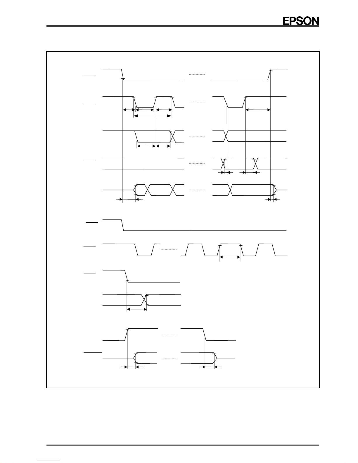
7.2. Timing Chart
tps
tDSO
90 %
1
8
1
10 %
10 %
90 %
10 %
tDPZ2
tDPZ1
90 %
90 %
10 %
90 %
90 %
90 %
90 %
10 %
10 %
10 %
10 %
tSWR tHWR
tDSZ2
tHCS
tWCKH
tWCKL
tSCS 1/f CLK
tHD
tSD
tDSZ1
CS0
SCK
SIN
WR
SOUT
CS0
SCK
SCK
SOUT
CS1
TPOUT
Downloaded from Elcodis.com electronic components distributor
RTC – 4553AC
Page - 7 MQ - 342 - 01
8. How to use
8.1. Registers
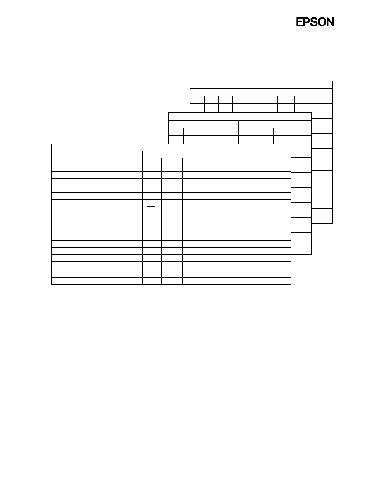
8.1.1. Register Table
* In positive logic, "H" on the data bus corresponds to "1" in the register.
"ADDRESS_F" of MODE 1 and MODE 2 is the same as "ADDRESS_F" of MODE 0.
Notes
(1) Do not set invalid (out of range) data for the time and calendar. Otherwise counting errors may occur.
(2) At power-on (before initialization), the data for each bit are cleared. Write the registers to set the values.
(3) Always set the D0 bit ( ∗bit) of the control register 2 to "0".
(4) When reading the D1 bit (— bit) of the control register 2, data of this bit are undefined.
(5) Always set the D3 bit (TEST bit) of the control register 3 to "0".
MODE 2 (User RAM register 2)
Address User RAM register
A3 A2 A1 A0 D3 D2 D1 D0
0 0 0 0 0 RA63 RA62 RA61 RA60
RA
64
RA
68
RA
72
RA
76
RA
80
RA
84
RA
88
RA
92
RA
96
RA
100
RA
104
RA
108
RA
112
RA
116
MS0
MODE 1 (User RAM register 1)
Address User RAM register
A3 A2 A1 A0 D3 D2 D1 D0
0 0 0 0 0 RA3 RA2 RA1 RA0
RA4
RA8
RA12
RA16
RA20
RA24
RA28
RA32
RA36
RA40
RA44
RA48
RA52
RA56
MS0
MODE 0
Address Counter control register
A3 A2 A1 A0 Register
designation D3 D2 D1 D0 Register name
0 0 0 0 0 S1 S8S4S2S11-second digit counter
1 0 0 0 1 S10 0 S40 S20 S10 10-second digit counter
2 0 0 1 0 MI1 mi8mi4mi2mi11-minute digit counter
3 0 0 1 1 MI10 0 mi40 mi20 mi10 10-minute digit counter
4 0 1 0 0 H1 h8h4h2h11-hour digit counter
5 0 1 0 1 H10 PM/
AM 0 h20 h10 10-hour digit counter
6 0 1 1 0 W 0 w4w2w1Day of the week digit counter
7 0 1 1 1 D1 d8d4d2d11-day digit counter
8 1 0 0 0 D10 0 0 d20 d10 10-day digit counter
9 1 0 0 1 MO1 mo8mo4mo2mo11-month digit counter
A 1 0 1 0 MO10 0 0 0 mo10 10-month digit counter
B 1 0 1 1 Y1 y8y4y2y11-year digit counter
C 1 1 0 0 Y10 y80 y40 y20 y10 10-year digit counter
D 1 1 0 1 CNT 1 TPS 30ADJ CNTR 24/ 12 Control register 1
E 1 1 1 0 CNT 2 BUSY PONC —∗Control register 2
F 1 1 1 1 CNT 3 SYSR TEST MS1 MS0 Control register 3
Downloaded from Elcodis.com electronic components distributor

RTC – 4553AC
Page - 8 MQ - 342 - 01
8.1.2. Register Bit Functions
Bit name Function
Bit marked "0" Unused bit that cannot be written. Always read as "0".
Second to year digit BCD code. Data are written using increment method.
PM/ AM "1" indicates PM and "0" indicates AM. This bit can be read also when 24-hour format is
selected (24/12=1). (AM: 00:00 to 11:59, PM: 12:00 to 23:59)
Day of the week digit
To be coded as 7-base counter.
Example Data 0 1 2 3 4 5 6
Coded da
y
of the week Sun. Mon. Tue. Wed. Thu. Fri. Sat.
Year digit Automatic leap year compensation up to 2099
User RAM area 30 ×4 bit SRAM
TPS
(Timing pulse selection)
Bit for selecting reference signal output
waveform.
Note 1/10 Hz is not output for 10 seconds
after power-on or system reset (output is
"L").
TPS bit Frequency (cycle time)
01024 Hz (976.5 µs)
1 1/10 Hz (10 s)
30ADJ
(30 seconds adjustment) Setting this bit to "1" performs 30 second adjustment.
The bit automatically resets when 30 second adjustment is completed (after 76.3 µs).
CNTR
(Counter reset) Setting this bit to "1" resets the time and calendar counters.
24/ 12 24-hour or 12-hour format selection bit. When set to "1", 24-hour format is used. When set
to "0", 12-hour format is used.
Busy
Used when reading/writing time and calendar counter data. Set to "1" when carry occurs.
BUSY bit Mode Meaning
0 No carry Time/calendar counter read/write possible
1 Carry Time/calendar counter read/write prohibited
PONC
(Power-on-clear detection)
At power-on, the power-on-clear function automatically sets this bit to "1". This has the
same effect as data initialization.
Register Data
Time/calendar counters 00-year, 01-month, 01-day, AM 12-hour,
00-minute, 00- second, 0-day of the week
Control registers All "0" (PONC = "1")
User RAM area Undefined
When PONC is "1", data must be set. First clear this bit (this can be done by writing "1" to
SYSR and then releasing system reset) and then set the time/calendar counters.
Bit marked " −" Cannot be written. When read, the data are undefined.
Bit marked " ∗" Can be written but must always be set to "0".
SYSR
(System reset)
At SYSR = "1" all logic bits are initialized. The SYSR bit is reset to "0" by causing an up
transition of CS0 and a down transition of SCK.
Register Data
Time/calendar counters 00-year, 01-month, 01-day, AM 12-hour,
00-minute, 00- second, 0-day of the week
Control registers All "0" (SYSR = "1")
User RAM area Undefined
TEST Epson test bit. Must be set to "0".
MS0, MS1
(Mode selection)
These 2 bits serve for mode selection.
MS1 MS0 Mode name Content
0 0 Mode 0 Time/calendar counters and control
registers 1 - 3
0 1 Mode 0 Time/calendar counters and control
registers 1 - 3
1 0 Mode 1 User RAM area (RA0- RA59) and control
register 3
1 1 Mode 2 User RAM area (RA60 - RA119) and
control register 3
Downloaded from Elcodis.com electronic components distributor

RTC – 4553AC
Page - 9 MQ - 342 - 01
8.2. Register Description
8.2.1. Time/Calendar Counter Registers
· In normal mode (CNTR = "0"), the counter is incremented by a write operation.
(1) Second digit counter
Counts values from 0 to 59. The counter can be read and incremented. When the second digit counter is
incremented, fractions below full seconds are reset. Therefore a carry occurs 1 second after the increment
operation is finished.
A3 A2 A1 A0 Name D3 D2 D1 D0 Register contents
0 0 0 0 S1 S8S
4S
2S
11-second digit counter
0 0 0 1 S10 0 S40 S
20 S
10 10-second digit
counter
(2) Minute digit counter
A3 A2 A1 A0 Name D3 D2 D1 D0 Register contents
0 0 1 0 MI1 mi8mi4mi2mi11-minute digit counter
0 0 1 1 MI10 0 mi40 mi20 mi10 10-minute digit counter
Counts values from 0 to 59. The counter can be read and incremented.
(3) Hour digit counter
A3 A2 A1 A0 Name D3 D2 D1 D0 Register contents
0 1 0 0 H1 h8h
4h
2h
11-minute digit counter
0 1 0 1 H10 PM/AM 0 h20 h
10 10-minute digit counter
Counts values from 0 to 23. The counter can be read, and the 1-hour digit counter can be incremented.
(The 10-hour digit counter cannot be incremented.)
D0 in the control register 1 sets the 12-hour/24-hour display format.
24/12 bit Displayed time
0 (12-hour format) AM 12:00 to AM 11:59, PM 12:00 to PM 11:59
1 (24-hour format) AM 00:00 to AM 11:59, PM 12:00 to PM 23:59
* PM/AM bit: This bit is output also when 24-hour format is selected.
* Time keeping is not affected also when the 12-hour/24- hour format is switched during clock operation.
(4) Day of the week digit counter
A3 A2 A1 A0 Name D3 D2 D1 D0 Register contents
0 1 1 0 W 0 w4w
2w
1Day of the week digit
counter
Counts values from 0 to 6. The counter can be read and incremented. The correspondence between count
value and day of the week is set by the user.
Example Data 0 1 2 3 4 5 6
Coded day of the week Sun. Mon. Tue. Wed. Thu. Fri. Sat.
(5) Day digit counter
A3 A2 A1 A0 Name D3 D2 D1 D0 Register contents
0 1 1 1 D1 d8d
4d
2d
11-day digit counter
1 0 0 0 D10 0 0 d20 d
10 10-day digit counter
The counter value is different depending on the month.
(a) For long months (1, 3, 5, 7, 8, 10, 12), the counter counts values from 1 to 31. The counter can be read
and incremented.
(b) For short months (4, 6, 9, 11), the counter counts values from 1 to 30. The counter can be read and
incremented.
(c) For February, the counter counts values from 1 to 29 if it is a leap year and from 1 to 28 in other years.
The counter can be read and incremented.
(6) Month digit counter
A3 A2 A1 A0 Name D3 D2 D1 D0 Register contents
1 0 0 1 MO1 mo8mo4mo2mo11-month digit counter
1 0 1 0 MO10 0 0 0 mo10 10-month digit counter
Counts values from 1 to 12. The counter can be read and incremented.
(7) Year digit counter
A3 A2 A1 A0 Name D3 D2 D1 D0 Register contents
1 0 1 1 Y1 y8y
4y
2y
11-year digit counter
1 1 0 0 Y10 y80 y
40 y
20 y
10 10-year digit counter
Counts values from 0 to 99 for the last two digits of the year. The counter can be read and incremented. Until
2099, leap year compensation is automatically provided. ('92, '96, '00, '04, '08, '12, '16, '20 ... are leap years.)
Downloaded from Elcodis.com electronic components distributor

RTC – 4553AC
Page - 10 MQ - 342 - 01
8.2.2. Control Registers
(1) Control register 1
A3 A2 A1 A0 Name D3 D2 D1 D0 Register contents
1 1 0 1 CNT 1 TPS 30ADJ CNTR 24/12 Control register 1
Control register 1 performs 12-hour/24-hour display format switching, digit counter reset, 30 second
adjustment, and timing pulse signal switching. The register allows data read and write.
(a) TPS bit (D3)
The TPS bit selects the timing pulse output waveform.
TPS bit Frequency (cycle) "L" level duty
0 1024 Hz (976.5 µs) 1/2 (488.28
µs)
1 1/10 Hz (10 s) 3/5 (6 s)
1/10 Hz is not output for 10 seconds after power-on or system reset (output is "L").
(b) 30ADJ bit (D2)
When "1" is written to this bit, one of the following reset operations is carried out.
Seconds digit before
adjustment Seconds digit after adjustment
29 seconds or less Seconds reset to "00" without carry to 1-minute
digit
30 seconds or more Seconds reset to "00" with carry to 1-minute digit
When "1" was written to the 30ADJ bit, the bit automatically resets itself to "0" within 76.3 µs The 30 second
adjustment function also resets fractions below full seconds. The TPOUT 1/10 Hz duty changes for one
cycle only during 30 second adjustment.
(c) CNTR bit (D1)
The CNTR bit resets the time/calendar counters.
CNTR bit Content
0 Normal mode (time/calendar counters can be incremented)
1 Selected counter is reset to "0"
* For counters other than the year, selecting either the 1 or the 10 digit counter will reset both counters.
When CNTR is used to reset the seconds, fractions below full seconds are also reset. The TPOUT 1/10
Hz duty changes for one cycle only during reset.
(d) 24/12 bit (D0)
The 24/12 bit serves to switch between 12-hour and 24-hour format.
24/12 bit Displayed time
0 (12-hour format) AM 12:00 to AM 11:59, PM 12:00 to PM 11:59
1 (24-hour format) AM 00:00 to AM 11:59, PM 12:00 to PM 23:59
* PM/AM bit: This bit is output also when 24-hour format is selected.
* Time keeping is not affected also when the 12-hour/24- hour format is switched during clock operation.
Downloaded from Elcodis.com electronic components distributor

RTC – 4553AC
Page - 11 MQ - 342 - 01
(2) Control register 2
A3 A2 A1 A0 Name D3 D2 D1 D0 Register contents
1 1 1 0 CNT 2 BUSY PONC — ∗Control register 2
Control register 2 provides flags for carry detect and power-on-clear detect.
(a) BUSY bit (D3)
The BUSY bit serves for time/calendar counter digit carry detection.
BUSY bit Mode Meaning
0 Normal mode Time/calendar counter read/write possible
1 Carry Time/calendar counter read/write prohibited
If the BUSY bit is "L", carry does not occur for at least 3.9 ms. (Also when read/write is carried out at point
"a" in the chart below, carry does not occur for 3.9 ms.)
Take the processing time into consideration and design the read/write operation to complete within 3.8 ms.
Clock read/write during carry
· Read It may not be possible to read correct data.
· Write Because the clock has priority, the write operation does not increment the counter.
(During carry, the result is the same as for a read operation.)
BUSY timing
Approx 0.5 µs
Carry pulse in IC Read/write possible Read/write prohibited (clock/calendar)
1 s 3.9 ms
“a”
BUSY bit
(b) PONC bit (D2)
The PONC bit is the power-on-clear detection bit (see next page). It is set to "1" when power-on-clear is
detected. The PONC bit is reset (1 →0) by setting the SYSR bit to "1".
(c) D1 bit (bit marked "—")
When this bit is read, data are undefined.
(d) D0 bit (bit marked " ∗")
When writing this bit, always set it to "0".
(3) Control register 3
Control registers 3 serves for reading and writing data for address mode switching and making system reset
settings.
The control register 3 applies to modes 0 - 2.
A3 A2 A1 A0 Name D3 D2 D1 D0 Register contents
1 1 1 1 CNT 3 SYSR TEST MS1MS0Control register 3
(a) SYSR bit (D3)
The SYSR bit serves for clearing all counter registers (see section on initialization on next page).
This bit is reset by making CS0 High and SCK Low.
(b) TEST bit (D2)
The TEST bit serves to switch the IC to the test mode.
Note Be sure to permanently set this bit to "0". Otherwise correct operation is not assured.
(c) MS1, MS0 bit (D1, D0)
The MS1 and MS0 bits serve for address switching.
MS1 MS0 Mode name Content
0 0 MODE 0 Time/calendar counters and control registers 1 - 3
0 1 MODE 0 Time/calendar counters and control registers 1 - 3
1 0 MODE 1 User RAM area (RA0- RA59) and control register 3
1 1 MODE 2 User RAM area (RA60 - RA119) and control register 3
Downloaded from Elcodis.com electronic components distributor

RTC – 4553AC
Page - 12 MQ - 342 - 01
8.3. How to use
8.3.1. Data Read
When CS0 is "L", the serial address data input at SIN is read at the leading edge of SCK . Next, when
WR = "H" is taken in on the 8th pulse leading edge of SCK the counter control register or RAM address is
selected. The data of the selected counter control register or RAM address are output in the following cycle
from SOUT, in sync with the SCK trailing edge.
8.3.2. Data Write/Modify
When CS0 is "L", the serial address data input at SIN is read at the leading edge of SCK . Next, when
WR = "H" is taken in on the 8th pulse leading edge of SCK , the counter control register or RAM address is
selected, and data are written as shown below.
Item Content
Time/calendar Counter, counter data increment (+1) *
Control register/RAM Serial address/lower 4 bit of data are written
The selected counter register or RAM address data are output in the following cycle from SOUT, in sync
with the SCK trailing edge.
* The hour digit counter can be incremented via the 1-hour digit counter.
8.3.3. Initialize
(1) System reset
When the SYSR bit in the control register 3 is set to "1", all logic bits are initialized. The SYSR bit is reset to
"0" by causing an up transition of CS0 and a down transition of SCK .
Register Data
Time/calendar counters - year, 01-month, 01-day, AM 12-hour, 00-minute,
00- second, 0-day of the week
Control registers All "0" (SYSR = "1")
User RAM area Undefined
Until system reset is released, TPOUT is fixed to "L".
1/10 Hz is not output for 10 seconds after system reset is released.
(2) Power-on-clear
At power-on, the power-on-clear function automatically performs a sequence identical to system reset.
However, because the PONC bit remains at "1", a system reset must be performed to set the PONC bit to
"0" before setting the time and calendar.
8.3.4. Timing Pulse Output
The timing pulse is output from the TPOUT pin.
Normally, a 1024 Hz signal is output. By setting the TPS bit in the control register 1 to "1", this can be switched
to 1/10 Hz.
•Switchover timing
SCK
8th leading edge of SCK
TPS Approx 60 µs
Switch from 1024 Hz to 1/10 Hz
Downloaded from Elcodis.com electronic components distributor

RTC – 4553AC
Page - 13 MQ - 342 - 01
8.3.5. Sample Operation Flow Charts
(1) Time/calendar initialize example
(Example for initialization through power-on-clear when battery was changed etc.)
YES
NO BUSY = 0?
END
30ADJ ←1
Increment 1-minute digit and
10-minute digit
Increment 1-hour digit
Set 24/12-hour format
Increment day of the
week digit
<
?
>
Increment 1-day digit and
10-day digit
Increment 1-month digit and
10-month digit
Increment 1-year digit and
10-year digit
SYSR ←1
START
•Release PONC bit = "1" (1 →0)
•While BUSY = "1", a carry operation is in progress
and the setting should not be carried out. The
following processing steps must be completed within
996 ms after SYSR ← "1" or after the BUSY bit down
transition was detected. If the process takes longer,
the BUSY bit must be checked again for continued
processing.
•It is advisable to start the setting from the year digit,
to prevent setting nonexistent data.
•When the 1-digit of the year, month, day, hour,
minute, or second is set, carry to the 10-digit can
occur.
•It is advisable to set this before setting the hour digit,
to prevent setting nonexistent data.
•Set the 10-hour digit by incrementing the 1-hour
digit.
(2) Time/calendar modify example (8:00 →12:00)
BUSY = 0?
NO
YES
END
Increment 1-hour digit
(4 times)
START MS0=0, MS1=0
While BUSY = "1", a carry operation is in progress and
the setting should not be carried out.
4 times (8 →9 →10→11→12)
↑
10-hour digit is automatically carried.
The processing should be completed within 3.8 ms after
detecting BUSY = "0".
Downloaded from Elcodis.com electronic components distributor

RTC – 4553AC
Page - 14 MQ - 342 - 01
(3) Time/calendar modify example using
counter reset (8:00 →2:00) (4) RAM write example
NO
MS0="0", MS1="0"
END
( 0 →1 →2 )
( 8 →0 )
YES
BUSY = 0?
Increment 1-hour digit
(2 times)
CNTR ←0
Write hour digit
CNTR ←1
START
Write to RAM in MODE 1
START
END
Write to RAM in MODE 1
MS0←1
MS1←1
MS0←0
MS1←1
Set MODE 2
Set MODE 1
Note 1 If processing is not completed within 3.8 ms, check the BUSY bit again.
Note 2 Reset (CNTR ←"1") applies to the digits for which writing was performed [1-hour digit and 10-hour
digit in example (3)]. Consequently, to change the setting from 11:00 to 2:00, the hour digit must be
reset (CNTR →"1").
For the year, CNTR is used separately for the 1-year digit and 10-year digit. Performing CNTR on the
1-year digit does not change the 10-year digit. Conversely, performing CNTR on the 10-year digit does
not change the 1-year digit.
(5) Time/calendar read example (6) RAM read example
END
YES
YES
PONC=0? NO
NO BUSY = 0?
Read time/calendar
START
If BUSY = "0", there will
be no carry for at least
3.8 ms.
If PONC = "1", initialization was
carried out and data must be set
again
MS0←0
MS1←0
Read MODE 2 RAM
Read MODE 1 RAM
END
Set MODE 2
Set MODE 1
MS0←0
MS1←1
MS0←1
MS1←1
YES
PONC=0? NO
START
If PONC = "1", initialization was
carried out and data must be set
again
MS0←0
MS1←0
Downloaded from Elcodis.com electronic components distributor

RTC – 4553AC
Page - 15 MQ - 342 - 01
(7) Time/calendar read example using BUSY bit down transition
Read time/calendar
PONC=0?
Time and calendar read interval is 996 ms.
END
YES
YES
PONC=0? NO
NO
NO
BUSY = 1?
START
If PONC = "1", initialization was
carried out and data must be set
a
g
ain
MS0←0
MS1←0
8.3.6. CS1 and CS0 Operation
When designing a floating arrangement, take the following into consideration. CS0 can be floating while CS1
= "L", but CS1 can never be floating. (Otherwise a through current would flow, leading to increased current
consumption during operation on backup battery power.) When CS1 = "L", input is disabled, and SOUT and
TPOUT are at high impedance.
To internal circuits
To internal circuits
To internal circuits
To internal circuits
From internal circuits
From internal circuits
CS1
CS0
WR
SCK
SIN
SOUT
TPOUT
8.3.7. System Power Down During Interface Operation
When the system power goes down during interface operation with the CPU, causing CS1 to become "L", the
incomplete data will be invalid. Immediately after system power restoration, when CS1 has become "H", the
output data from SOUT are undefined for one cycle.
8.3.8. Power Supply and CS1 Operation
When the system power is shut down, VDD falls to the battery voltage. When used at VDD ±10%, CS1 must be
set to "L" before VDD crosses point <A> in the diagram below. When system power is restored, CS1 must be
set to "H" before VDD crosses point <B>.
System power on/off time chart
System power
Access disabled
Power down
Battery voltage
<A> VDD-20 % <B>
CS1
VDD 5 V
Downloaded from Elcodis.com electronic components distributor
RTC – 4553AC
Page - 16 MQ - 342 - 01
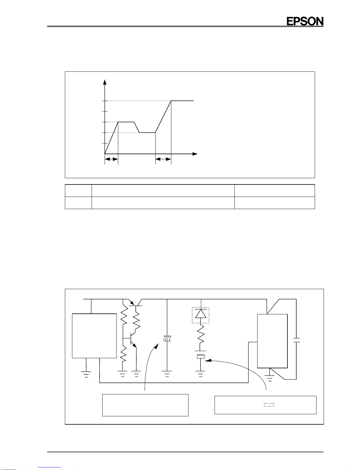
8.3.9. Power-On Reset
When the system power is turned on, the power-on reset function operates automatically, performing a
sequence identical to system reset. However, because the PONC bit remains at "1", a system reset must be
performed to set the PONC bit to "0" before setting the time and calendar.
The conditions for power-on reset and the conditions for data retention and normal IC operation during power
fluctuation are shown below.
t1: Condition for power-on reset
t2: Condition for data retention and normal
IC operation during power-on
Note: 3 V and 5 V are recommended
voltages. 2 V is the backup voltage.
VDD
t1
5
[ V ]
4
3
2
1
0
t2t
Ta = −30 °C to +70 °C
t 1 Condition tR for power-on reset
at 0+0.3 V →3 V or 0+0.3 V →5 V (Note 1) 1.0 µs/V ≤tR ≤1.6 ms/V
t 2 Condition tR for no power-on reset
at 2 V →3 V or 2 V →5 V (Note 2) 1.0 µs/V ≤tR ≤1.6 ms/V
Note 1 The voltage level before initial power-on should be 0.3 V or less. If powering up from an intermediate
potential, power-on reset may not be performed correctly. Be sure to verify correct operation.
Note 2 Within the voltage range for data retention and clock operation (2.0 V - 5.5 V), power-on reset is designed
not to be performed under the above conditions, to prevent data loss. When the voltage level falls below 2
V, operation and data retention are no longer assured.
Note 3 During power-on or power restoration from an intermediate potential outside of the assured operation
range (0.3 V - 1.9 V), the power-on reset circuit will not operate normally, leading to possible malfunction. If
the backup battery voltage has fallen below 2.0 V, the VDD pin of the RTC must be temporarily set to
ground potential before restoring the power.
8.3.10. Power Supply Connection Example
Use a high capacitance value here to guard
against reverse current flowing from the collector
to the emitter of the transistor during transition
from power on to power off.
Power-down
detection circuit
0.1 µF
GND
CS1
VDD
RTC
+
R
+
+5 V+5 V +VCE
Secondary battery or lithium battery. (Lithium batter
y
requires the diode shown in . Regarding the value o
f
the resistor R, consult the battery manufacturer.
Downloaded from Elcodis.com electronic components distributor

RTC – 4553AC
Page - 17 MQ - 342 - 01
8.3.11. Processing of Non-Existent Data
(1) If the month digit is incremented while the current setting is January 31, a non-existent setting will result
(February 31). Carry from the hour digit will cause this setting to become March 1.
Month digit
incremented Carry from hour digit
Jan. 31 →Feb. 31 →Mar. 01
(2) If the year digit is incremented while the current setting is February 29 of a leap year, a non-existent setting will
result (February 29 of a non-leap year). Carry from the hour digit will cause this setting to become March 1.
Year digit
incremented Carry from hour digit
Feb. 29 00 →Feb. 29 01 →Mar. 01 01
When the following non-existent data are set (February 30), incrementing the 10-day digit causes an overflow in
the 10-day digit, clearing the 1-day digit.
10-day digit
incremented once 10-day digit
incremented once
Feb. 30 →Feb. 00 →Feb. 10
Feb. 29 →Feb. 01
When a valid date is set, overflow of the 10-day digit does not clear the 1-day digit.
(3) When the 10-day digit is incremented past "31", the day digit counter becomes "01".
(4) When the 10-month digit is incremented, the month digit overflow processing will differ according to the month.
10-month digit incremented once
00 month Oct.Non-existent
month →
Oct. 00 month
→Non-existent
month
Nov. →Jan.
Dec. →Feb.
Mar. - Sep. →Jan.
Downloaded from Elcodis.com electronic components distributor
Table of contents


