Seiko Epson S5U1C17702T1100 User manual

CMOS 16-BIT SINGLE CHIP MICROCOMPUTER
(Software Evaluation Tool for S1C17702)
S5U1C17702T1100
Hardware Manual

Evaluation board/kit and Development tool important notice
1. This evaluation board/kit or development tool is designed for use for engineering evaluation, demonstration,
or development purposes only. Do not use it for other purpose. It is not intended to meet the requirement of
design for finished product.
2. This evaluation board/kit or development tool is intended for use by an electronics engineer, and it is not the
product for consumer. The user should use this goods properly and safely. Seiko Epson dose not assume any
responsibility and liability of any kind of damage and/or fire coursed by usage of it. User should cease to use
it when any abnormal issue occurs even during proper and safe use.
3. The part used for this evaluation board/kit or development tool is changed without any notice.
NOTICE
No part of this material may be reproduced or duplicated in any form or by any means without the written
permission of Seiko Epson. Seiko Epson reserves the right to make changes to this material without notice.
Seiko Epson does not assume any liability of any kind arising out of any inaccuracies contained in this material
or due to its application or use in any product or circuit and, further, there is no representation that this material is
applicable to products requiring high level reliability, such as, medical products. Moreover, no license to any
intellectual property rights is granted by implication or otherwise, and there is no representation or warranty that
anything made in accordance with this material will be free from any patent or copyright infringement of a third
party. When exporting the products or technology described in this material, you should comply with the
applicable export control laws and regulations and follow the procedures required by such laws and regulations.
You are requested not to use, to resell, to export and/or to otherwise dispose of the products (and any technical
information furnished, if any) for the development and/or manufacture of weapon of mass destruction or for other
military purposes.
All brands or product names mentioned herein are trademarks and/or registered trademarks of their respective
companies.
©SEIKO EPSON CORPORATION 2012, All rights reserved.

Devices
S1 C 17xxx F 00E1
Packing specifications
00 : Besides tape & reel
0A : TCP BL 2 directions
0B : Tape & reel BACK
0C : TCP BR 2 directions
0D : TCP BT 2 directions
0E : TCP BD 2 directions
0F : Tape & reel FRONT
0G : TCP BT 4 directions
0H : TCP BD 4 directions
0J : TCP SL 2 directions
0K : TCP SR 2 directions
0L : Tape & reel LEFT
0M : TCP ST 2 directions
0N : TCP SD 2 directions
0P : TCP ST 4 directions
0Q : TCP SD 4 directions
0R : Tape & reel RIGHT
99 : Specs not fixed
Specification
Package
D: die form; F: QFP, B: BGA
Model number
Model name
C: microcomputer, digital products
Product classification
S1: semiconductor
Development tools
S5U1 C 17000 H2 1
Packing specifications
00: standard packing
Version
1: Version 1
Tool type
Hx : ICE
Dx : Evaluation board
Ex : ROM emulation board
Mx : Emulation memory for external ROM
Tx : A socket for mounting
Cx : Compiler package
Sx : Middleware package
Corresponding model number
17xxx: for S1C17xxx
Tool classification
C: microcomputer use
Product classification
S5U1: development tool for semiconductor products
00
00
Configuration of product number

Table of Contents
S5U1C17702T1100 HARDWARE MANUAL EPSON i
(SOFTWARE EVALUATION TOOL FOR S1C17702)
- Table of Contents -
1 Features .......................................................................................................................... 1
2 Components Included in the Package
......................................................................... 2
3 Name and Functions of Each Part ............................................................................... 3
3.1 Name of Each Part ............................................................................................................ 3
3.2 Dimensions of the Boards ................................................................................................. 4
3.2.1 Dimensions of the CPU Board ............................................................................ 4
3.2.2 Dimensions of the ICD Board ............................................................................. 5
3.2.3 Dimensions of the LCD Panel Board .................................................................. 6
3.3 Main Parts ......................................................................................................................... 8
3.4 Functional Description of Each Part .................................................................................. 9
3.4.1 ICD board ........................................................................................................... 9
3.4.2 CPU board .......................................................................................................... 9
4 Block Diagrams ............................................................................................................ 10
5 Operating Environment and Start-Up Procedures .................................................... 11
5.1 Simple Software Development Environments .................................................................. 11
5.2 Standalone Operation of SVT17702 ................................................................................ 14
5.3 ICD Board Firmware Update Procedures ........................................................................ 14
6 Differences between ICD Board and ICD Mini ........................................................... 15
7 I/O Ports ......................................................................................................................... 16
8 Setting Switches
........................................................................................................... 17
8.1 Setting for SW6 ................................................................................................................ 17
8.2 Setting for SW8 ................................................................................................................ 18
8.3 Setting for SW9 ................................................................................................................ 18
9 Key Input Circuit on the CPU Board ........................................................................... 19
10 Infrared Emitting Diode/Receiver Module ................................................................ 20
10.1 Emitting and Receiving Light at Infrared Area ................................................................ 21
10.2 Power Supply Switch for Infrared Transmitter Module ................................................... 21
11 LCD Panel .................................................................................................................... 22
11.1 Segments and Commons of the LCD Panel ................................................................... 22
12 Serial Ports .................................................................................................................. 23
13 External Input for OSC3 ............................................................................................. 24
14 Expansion Interface ................................................................................................... 25
14.1 JICD Connector .............................................................................................................. 26
14.2 JEX Connector ............................................................................................................... 27
14.3 JEX2 Connector ............................................................................................................ 28
14.4 JRIF Connector .............................................................................................................. 29
14.5 Switching the SPI Port Connector .................................................................................. 30
Appendix A How to Measure Current Consumption ........................................................31

1 Features
S5U1C17702T1100 HARDWARE MANUAL EPSON 1
(SOFTWARE EVALUATION TOOL FOR S1C17702)
1 Features
S5U1C17702T1100 (Software evaluation Tool for S1C17801. Hereafter referred to as SVT17702)is an evaluation
board for S1C17702 manufactured by SEIKO EPSON.
The SVT17702 consists of two circuit boards: CPU and LCD boards. By connecting these boards, the SVT17702
allows the user to debug the application software without an ICD or other debugging tools.
In addition, it provides extended interfaces such as serial ports, allowing you to connect your own expansion boards
to the SVT17702.
<CPU Board>
CPU S1C17702
Input power voltage +3.3 VDC (supplied through the ICD interface or CR2032 coin cell battery)
CPU input clock OSC1: 32.768 kHz
OSC3: 6 MHz
On-board functions/devices ・Reset switch
・Expansion interface connectors (GPIO, UART, I2C and SPI)
・ICD board connector
・Key input circuit (4 keys)
・Rotary encoder with switch
・Infrared transmitter LED/Receiver module
・ STN LCD panel (display size: 32 commons x 128 segments, black &
white)(32 commons and 72 segments can be driven)
<ICD Board>
PC interface USB 1.1
Power supply voltage USB bus power (On-board regulator output voltage of 3.3 V)
On-board functions/devices ・Tri-color status LED
・Reset switch
・CPU board connector

2 Components Included in the Package
2 EPSON S5U1C17702T1100 HARDWARE MANUAL
(SOFTWARE EVALUATION TOOL FOR S1C17702)
2 Components Included in the Package
The S5U1C17702T1100 package contains:
(1) SVT17702 CPU board (evaluation board) .................... 1
(2) SVT17702 ICD board ................................................... 1
(3) USB cable .....................................................................1
(4) Coin cell battery (CR2032/3V) .....................................1
(5) Warranty Registration Card ...........................................1 each for English/Japanese
(6) Warranty Card ............................................................... 1 each for English/Japanese
(7) Precautions in Use .........................................................1 each for English/Japanese
(8) Manual Download Guide ..............................................1 each for English/Japanese

3 Name and Functions of Each Part
S5U1C17702T1100 HARDWARE MANUAL EPSON 3
(SOFTWARE EVALUATION TOOL FOR S1C17702)
3 Name and Functions of Each Part
3.1 Name of Each Part
The following describes name and functions of each part:
Figure 3.1.1 Parts Mounted on the Front Side of the Board
(1) LED(RGB) (6) Rotary encoder (11) CPU board reset switch
(2) SW4(7) SW2(12) Expansion board connector (JEX2)
(3) Crystal oscillator (6MHz/32kHz) (8) SW1(13) Expansion board connector (JEX)
(4) SW3(9) Infrared receiver module (14) ICD board reset switch (SW1)
(5) S1C17702 (10) Infrared transmitter module (15) miniB USB connector
Figure 3.1.2 Parts Mounted on the Back Side of the Board
(1) Rotary encoder
(2) ICD board to CPU board connector (JICD)
(3) Battery socket
(4) Expansion board connector (JRIF) (Not mounted)
CPU boardICD board
(1) (2) (4)
(3)
(5) (6) (7) (8)
(13)
(12)(9)
(10)
(11)
(14)
(15)
Dot matrix STN LCD panel
CPU board ICD board
(1)
(4) (3) (2)
3 Name and Functions of Each Part
4 EPSON S5U1C17702T1100 HARDWARE MANUAL
(SOFTWARE EVALUATION TOOL FOR S1C17702)
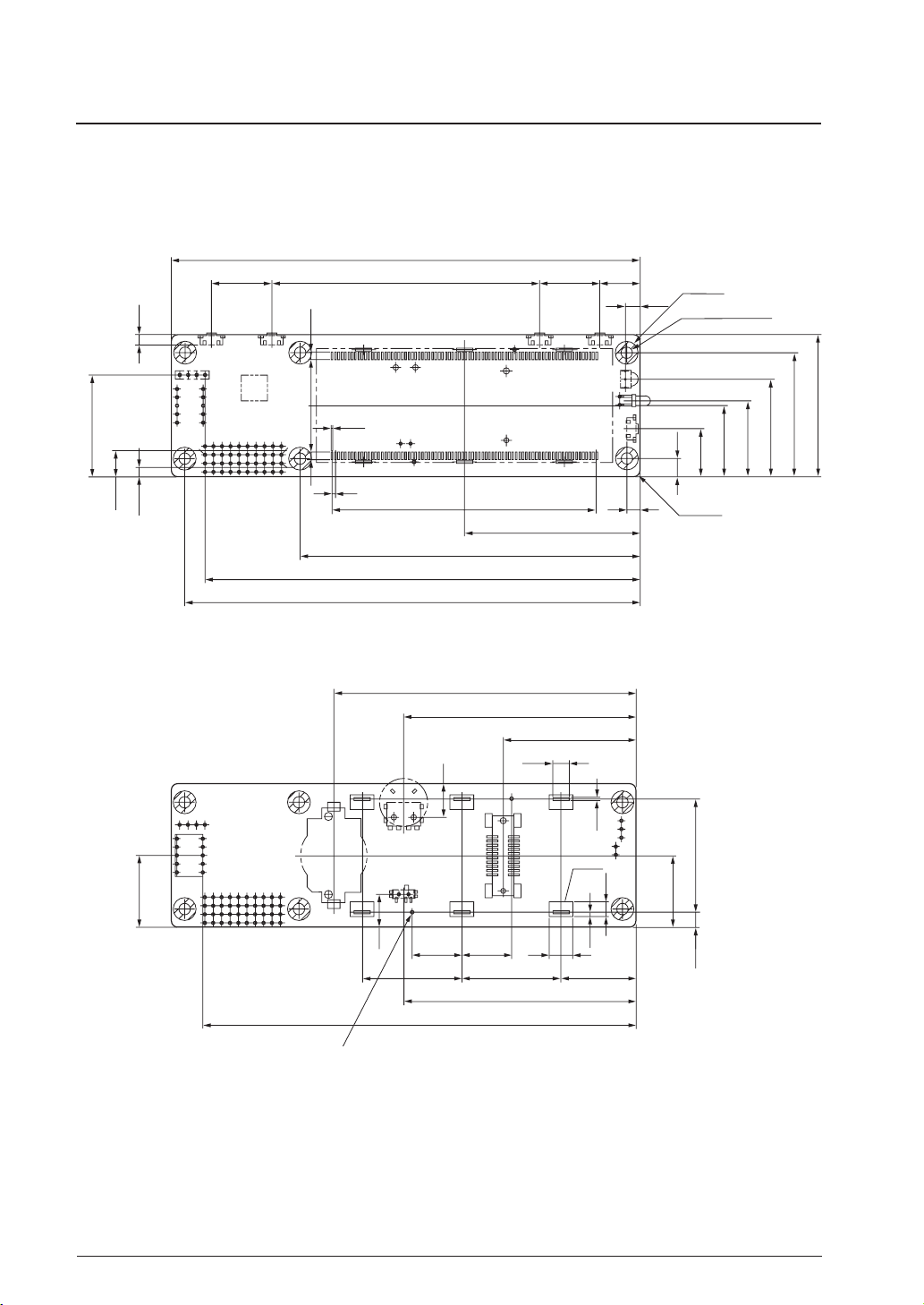
3.2 Dimensions of the Boards
3.2.1 Dimensions of the CPU Board
The following drawings show the dimensions of the CPU board.
<Top view>
101.5
130
140
80
0.5
18 18 12
79
1
4
52.5
136
2.77
7.85
30.77
28 2.3
2.3
5.5
23
43
14.5
21.5
29.5
37.5
3.1
CPU
JEX2
SW3 SW2 SW1
SW5
AN333
GP6UX311QS
SW4
1
14
2 1
160
212 1
1
2
2
JMINI
LCD
80
81
4.5
19
19
20
20
1
1
2
2
1
4-R2
Vcc
GND
VOUT
JEX
6-φ7
6-φ3.3 hole
Figure 3.2.1.1 Dimensions of the CPU Board (Front)
<Bottom view>
91
70
40
5.2
15
30 30
70
130.61
22.5
15 7
2-φ1.2 hole
4.55
1.3
4.5 0.8
10
10
33.9
21.5
21.5
land
10
2 1
9
JICD V1
SW6
SW7
B C S A 19 20
21
JRIF
13 +3
2
−
Figure 3.2.1.2 Dimensions of the CPU Board
∗ Precautions
• All dimensions are in millimeters (mm).
• Board thickness: 1.6 mm.

3 Name and Functions of Each Part
S5U1C17702T1100 HARDWARE MANUAL EPSON 5
(SOFTWARE EVALUATION TOOL FOR S1C17702)
3.2.2 Dimensions of the ICD Board
The following drawings show the dimensions of the ICD board.
<Top view>
4
21.5
37.5
43
50
4-φ3.5 through hole
4-R2
44-φ7 land
5.5
9
JUSB
15
Figure 3.2.2.1 Dimensions of the ICD Board (Front)
<Bottom view>
4.95
JICD
1
2
9
10
Figure 3.2.2.2 Dimensions of the ICD Board (Back)
∗ Precautions
• All dimensions are in millimeters (mm).
• Material: FR4, Board thickness: 1.6 mm
3 Name and Functions of Each Part
6 EPSON S5U1C17702T1100 HARDWARE MANUAL
(SOFTWARE EVALUATION TOOL FOR S1C17702)
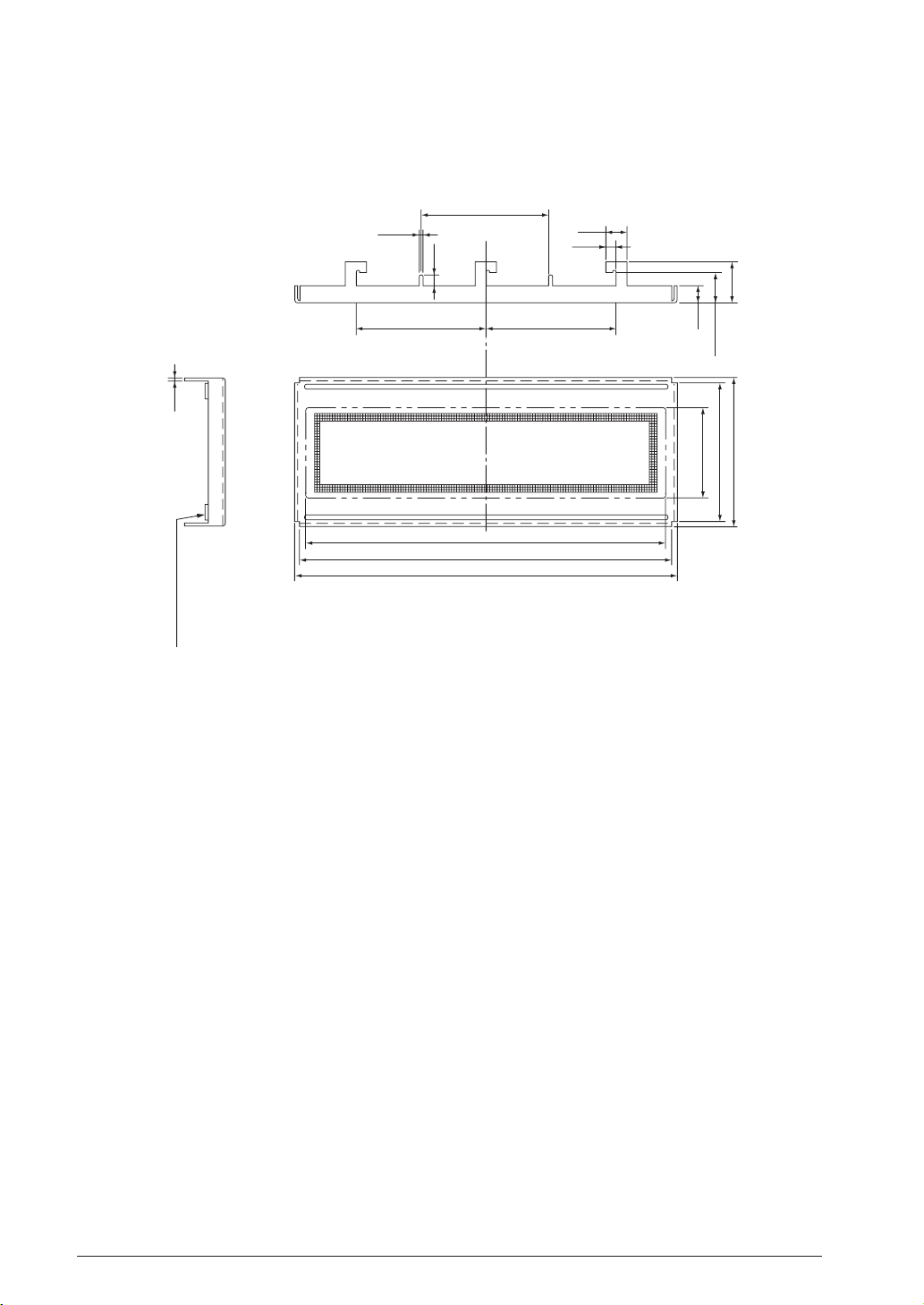
3.2.3 Dimensions of the LCD Panel Board
The following drawings show the dimensions of the LCD panel OPTO0569NG manufactured by Casil Optoelec-
tronic Product Development Ltd.) that is to be mounted on the LCD board.
(Excerpts from the Specifications of Casilʼs OPTO0569NG)
29.5±0.1
2–1.0
2.5
5.0
2.5
30.0±0.1 30.0±0.1
9.5±0.1
7.0±0.1
4.0
0.6
83.15(V.A.)
128 x 32 DOTS
86±0.2
88.4±0.2
34.5±0.2
32.1±0.2
20.75(V.A.)
ELASTOMER
(ZEBRA CONNECTOR)
Figure 3.2.3.1 LCD Panel Dimensions of LCD, Bezel and Zebra (Elastomer Connector)
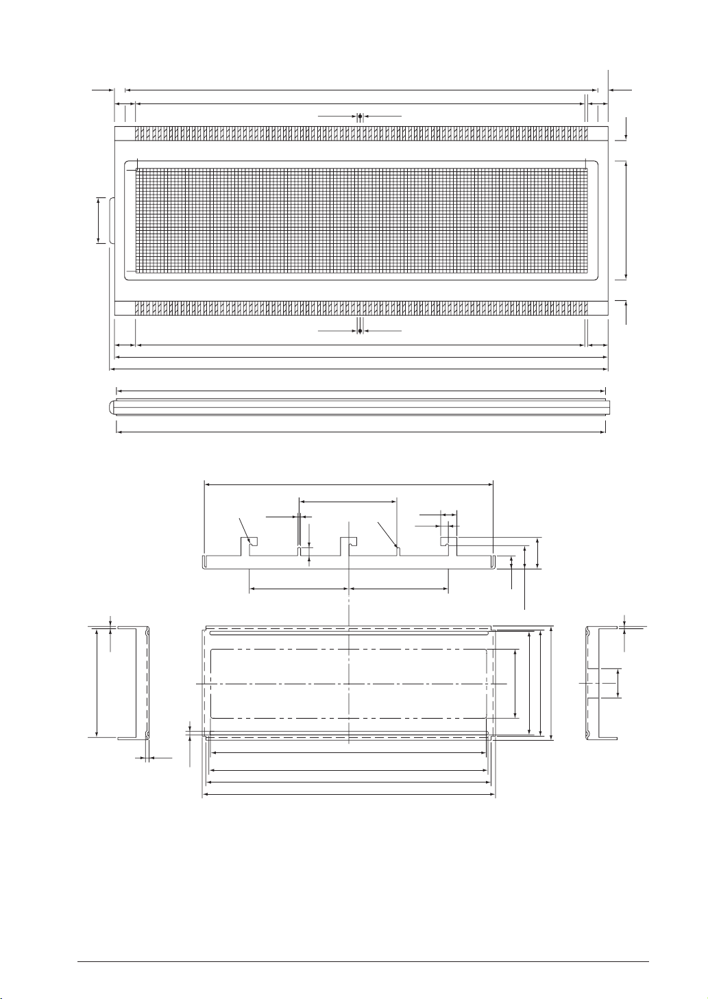
3 Name and Functions of Each Part
S5U1C17702T1100 HARDWARE MANUAL EPSON 7
(SOFTWARE EVALUATION TOOL FOR S1C17702)
83.15 MIN VIEWING AREA
( 1.0 X 79 = 79.0 )
( 1.0 X 79 = 79.0 )
0.5±0.050.5±0.05
0.5±0.050.5±0.05
1.92
MAX
8.0 MAX
(1.92)
3.75±0.2
3.75±0.2
1
S1
C1
C16
81
80
(3.75)
(3.75)
(3.63)
20.75
MIN VIEWING AREA
3.63
160
86.0±0.2 ATTACHED REAR REFLECTIVE
86.0±0.2 ATTACHED FRONT TRANSMISSIVE
87.8 MAX INCLUDING SEAL
87.0±0.2
S128
Figure 3.2.4.2 Dimensions of the LCD Panel
87.2 +0.1
0
–
29.5±0.1
2–1.0
2–1.0
2.5
R0.5
R0.5
5.0
2.5
30.0±0.1 30.0±0.1
9.5±0.1
9.0±0.5
7.0±0.1
4.0
0.6
33.3 +0.1
–0
1.0
0.6
83.15(V.A.)
83.6±0.3
86±0.2
88.4±0.2
34.5±0.2
32.1±0.2
31±0.3
20.75(V.A.)
Figure 3.2.4.3 Dimensions of the Bezel

3 Name and Functions of Each Part
8 EPSON S5U1C17702T1100 HARDWARE MANUAL
(SOFTWARE EVALUATION TOOL FOR S1C17702)
3.3 Main Parts
<CPU Board>
CPU (U3) S1C17702 SEIKO EPSON CORP.
Crystal oscillator(32.768kHz) (X1) FC-255 EPSON TOYOCOM CORP.
Crystal oscillator(6MHz) (X2) MA-406 EPSON TOYOCOM CORP.
Reset switch (RESET SW) (SW5) SKQTLCE010 ALPS
LCD panel Customized product CASIL OPTOELECTRONIC
PRODUCT DEVELOPMENT LTD
Expansion board connector (JEX) SLW-110-01-G-D SAMTEC
Expansion board connector (JEX2) SLW-110-01-G-D SAMTEC
Expansion board connector (JICD) PS-10SD-D4T1-1 JAE
Expansion board connector (JRIF) (not mounted)
8913-020-178MS-A-F KEL
Key switches (SW1 - SW4) SKRAAKE010 ALPS
Rotary encoder with switch (SW7) SIQ-02FVS3 MITSUMI
Infrared transmitter module (D2) AN333 STANLEY
Infrared receiver module (U1) GP6UX311QS SHARP
Infrared receiver module (replacement for U1)
PNA4702M Panasonic
Battery holder (V1) 1060 KEYSTONE
Coin cell battery CR2032(3V) maxell
<ICD Board>
USB miniB connector 54819-0572 molex
LED (RGB) 598-9920-307F Dialight
Reset switch (RESET SW) (SW1) SKRAAKE010 ALPS

3 Name and Functions of Each Part
S5U1C17702T1100 HARDWARE MANUAL EPSON 9
(SOFTWARE EVALUATION TOOL FOR S1C17702)
3.4 Functional Description of Each Part
3.4.1 ICD board
The ICD board is a hardware tool (emulator) to facilitate the development of software for the S1C17702. It controls
communication between your PC and the target IC (S1C17702) on the CPU board, providing a simple software
development environment for S1C17702. For information about its functional differences from the ICD Mini
(S5U1C17001H), a development tool supporting all S1C17 core product models, see Chapter 6.
ICD Board Reset Switch
Pressing the reset switch (SW1) on the ICD board reboots firmware on the ICD board and outputs the target
reset signal (#RESET_OUT) to the CPU board. This establishes the communication connection between the
CPU board and the ICD board if they are physically connected. If the CPU board and the ICD board are not
connected physically, the ICD board waits for a connection for communication.
ICD Board LED
The LED indicates ICD board and target statuses in different colors.
● (Blue) Power on (before the initial connection with the target is established.)
● (Green) The target is currently in debug mode.
● (Red) The target is not connected, or not properly connected.
The target is currently executing a user program.
3.4.2 CPU board
The CPU board is a simple target evaluation board equipped with the target CPU (S1C17702). It also contains vari-
ous peripheral functions and circuits, such as LCD panel and remote control transmitter/receiver module. It can be
used to develop and evaluate software for controlling these components.
CPU Board Reset Switch
Pressing the CPU board reset switch (SW5) resets the CPU board.
Coin cell battery
A holder for the coin cell battery (CR2032) is mounted on the back side of the CPU board. If the CPU board is
used alone, power is supplied from the coin cell battery.If the SVT17702 is used with the ICD board connected,
the switch circuit on the CPU board automatically supply power to the SV17702 from the ICD board.Power
supply from the coin cell battery is then automatically turned off.
∗ Inserting and removing coin cell battery
Insert the coin cell battery inside the battery holder on the back side of the CPU board with the (+) plus side
facing up.
(1) Slide the battery under the contact.
(2) Press into position until it clicks
into the locked position.
CR 2032
Figure 3.4.2.1 Installing Coin Cell Battery
If the battery cannot be easily removed, insert a thin rod or any other appropriate tool between the battery and
the battery holder and lift it out of the holder. Use care not to damage any contact of the holder and any part
mounted on the board.

4 Block Diagrams
10 EPSON S5U1C17702T1100 HARDWARE MANUAL
(SOFTWARE EVALUATION TOOL FOR S1C17702)
4 Block Diagrams
Figure 4.1 shows a block diagram for the CPU board of the SVT17702 and Figure 4.2 shows a block diagram for
the ICD board on the SVT17702.
<CPU board>
2.54mm pitch x 2 row
through hope
Extension
circuit
GND
ICD connector
(board to board)
Coin
Cell
DotMtx LCD
Drive : com x 72seg
LCD Dr GPIO
SPI
REMC
S1C17702
(BDA)
Debug i/f
JEX, JEX2
(GPIO i/f
UART i/f
I2C i/f
SPI i/f)
Key
(4)
Extension
circuit
2.54mm pitch x 2 row x 2
througn hole
REMC
communication
JRIF connector
(GPIO i/f)
REMC
i/f
Debug
i/f
OSC1
32kHz
OSC3
6MHz
PW
SW Reset
(SW)
VDD
GPIO
I2C UART
Panelspecification :
32com x 128seg
Figure 4.1 Block Diagram for CPU Board
<ICD board>
Host PC
USB 1.1
Regulator
5V->3.3V
Regulator
5V->1.8V
S1C33E07
5V
500mA
Max.
USB1.1 CPU Board
Flash ROM
3-color
LED x1
OSC3
48MHz
Figure 4.2 Block Diagram for ICD Board

5 Operating Environment and Start-Up Procedures
S5U1C17702T1100 HARDWARE MANUAL EPSON 11
(SOFTWARE EVALUATION TOOL FOR S1C17702)
5 Operating Environment and Start-Up
Procedures
By connecting with your PC via the ICD board, the SVT17702 can be operated in accordance with commands ex-
ecuted from a debugger on the PC. The SVT17801 is capable of operating the CPU board alone without using the
ICD board and PC. The following sections describe the connection and startup procedures to perform each respec-
tive operation.
5.1 Simple Software Development Environments
The SVT17702 provides a simple development environment of S1C17702 software using the CPU board as a tar-
get. This can be achieved by connecting the SVT17202 to your PC via the ICD board and using it with an S1C17
development tool on the PC (such as GNU17 IDE, compiler and debugger included in the S5U1C17001C package).
USB cable
ICD board
PC
(GDB17)
C17
702
JEX2 connecta
JEX connecta
LCD panel
Figure 5.1.1 Simple Software Development Environment
Operations under simple software development environment
Under this operating environment,the target CPU (the S1C17702 on the CPU board) operates according to
commands executed from a debugger on your PC connected with the ICD board.A command executed from the
debugger is sent to the ICD board via USB and, when it has been analyzed, converted into an S1C17702 debug
signal, after which it is sent to the CPU board.The debugger on your PC can be used to download programs or
data to the CPU board, or debug programs by controlling their execution and stop.
CPU operating mode
A BRK instruction or debug interrupt (such as forcible break with the debugger) from the ICD board causes the
target CPU (the S1C17702 on the CPU board) to stop executing the target program and enter into debug mode (or
break state).In this state, commands can be executed from the debugger on your PC.The LED on the ICD board
lights in green during debug mode.The state in which the target CPU is executing a target program is called
normal mode.The LED on the ICD board lights in red during normal mode.
Connection and start-up
The procedures for making connections and for starting up the SVT17702 to implement a simple software
development environment are described below.
(1) Connect the ICD board with the CPU board. (Connect the 10-pin connector on the JICD board to the
matching connector on the CPU board as shown in the connection diagram in Chapter 14.)
(2) Connect the ICD board to your PC via a USB cable.
(3) When the USB Driver Installation Wizard appears on your PC, install an appropriate driver.(This step is
required only for the first connection. It is not required for the second connection and afterward.)For the
installation procedure, see the later section “Installing USB driver”.
(4) Make sure that the color of the LED on the ICD board changes from blue to green (the target is in debug
mode).
(5) Start the IDE on you PC. When the GDB is automatically started by the IDE, have it run the program.
Make sure that the color of the LED on the ICD board changes to red (the target is in normal mode).
For details on the operation of the debugger and debugging commands, see the “S5U1C17001C Manual (S1C17
Family C Compiler Package).”

5 Operating Environment and Start-Up Procedures
12 EPSON S5U1C17702T1100 HARDWARE MANUAL
(SOFTWARE EVALUATION TOOL FOR S1C17702)
Note: Be sure NOT never to disconnect the USB cable between PC and ICD board while the debugger
is running.
Installing the USB driver
(1) When the SVT17702 is connected with the host computer via USB cable, the following screen appears.
(2) Follow the wizard to install the USB driver.
Press the Browse button and select “C:\EPSON\GNU17\utility\drv_usb” as the directory that contains the
USB driver.
∗ This path specifies where the IDE is installed.

5 Operating Environment and Start-Up Procedures
S5U1C17702T1100 HARDWARE MANUAL EPSON 13
(SOFTWARE EVALUATION TOOL FOR S1C17702)
When the USB driver has been installed successfully,you should see a list on the device manager similar to the
one shown below.
Note: If the USB driver is not listed as shown above, the driver should be reinstalled.

5 Operating Environment and Start-Up Procedures
14 EPSON S5U1C17702T1100 HARDWARE MANUAL
(SOFTWARE EVALUATION TOOL FOR S1C17702)
5.2 Standalone Operation of SVT17702
The SVT17702 allows the CPU board to operate standalone without using the ICD board or PC.
Standalone operation
In this operation environment, the S1C17702 on the CPU board operates in normal mode to execute a program
written in the built-in flash memory.Therefore, a user program must be downloaded into the flash memory
contained in the S1C17702 in advance.(The SVT17702 is shipped with a demo program preloaded into on-chip
flash memory.)(For information about how to download a user program to the on-chip flash memory, see the
"S5U1C17001C Manual (S1C17 Family C Compiler Package)".
Connection and start-up
The procedure for operating the SVT17702 in a standalone mode is described below.
(1) Turn on the PC(if it is turned off).
(2) While the ICD board is connected with the CPU board, connect your PC to the ICD board via USB cable.
(3) Start the debugger on your PC and download a user program to the on-chip flash memory on the S1C17702.
For information about downloading a program, see the “S5U1C17001C Manual (S1C17 Family C Compiler
Package).”
(4) After exiting the debugger, remove the USB cable to disconnect the ICD board from your PC.
(5) Disconnect the ICD board from the CPU board, and install a coin cell battery.
(6) Press the reset switch on the CPU board.Then the S1C17702 on the CPU board starts executing a user pro-
gram downloaded to the flash memory.
5.3 ICD Board Firmware Update Procedures
The SVT17702 can update the firmware of the ICD board using a debugger on your PC.The ICD board firmware
will be provided by EPSON if necessary.(An update file has an “.sa” extension.)
The procedure for updating firmware is described below.
Note: USB driver must be installed before starting firmware update.
(1) Connect the ICD board of the SVT17702 to your PC via USB cable.
(2) Press the reset switch on the ICD board (SW1).
(3) Start the debugger from the command prompt.
>cd c:¥EPSON¥gnu17 (Specify the directory path where the gnu17 is installed.)
>gdb
(4) When the debugger starts, enter the following commands.
(gdb) target icd usb
(gdb) c17 firmupdate path¥filename.sa
(where “path\filename.sa” is the update file name.)
(5) When the update process is complete, the LED on the ICD board lights up green(●).
(6) Press the reset switch on the ICD board to reboot the firmware.

6 Differences between ICD Board and ICD Mini
S5U1C17702T1100 HARDWARE MANUAL EPSON 15
(SOFTWARE EVALUATION TOOL FOR S1C17702)
6 Differences between ICD Board and
ICD Mini
Table 6.1 shows a comparison of specifications between the S5U1C17001H (ICD Mini) board, a development tool
for the S1C17 family, and the SVT17702 ICD board.While the SVT17702 contains the ICD mini interface (connector
not yet mounted), the ICD board and the ICD mini cannot be simultaneously connected. For information about how
to use the ICD mini, refer to the S5U1C17001H User Manual.
Table 6.1 Comparison of Functions between ICD Board and ICD mini
Product name S5U1C17000H
(ICD Mini)
S5U1C17702T1100(SVT17702)
ICD board
Core supported S1C17 core
Host interface USB 1.1
Frequency to communicate with the
target (DCLK frequency)
4kHz to 40MHz
Standalone flash programming
capability
Available Not available
Firmware update capability Available
Power supply for writing to flash ROM Available Not available
Reset signal output to target Available
Voltage associated with target system
I/O
3.3V, 1.8V, and voltage input from
target (1.0 to 5.0V)
3.3V
Connector for target 4ピン 10 pins
(including reset signal) *2
Power supply connector for writing to
flash ROM *3
4ピン –
∗1 Frequency supported when I/O interface voltage = 3.3V. Depending on ambient noise, temperature conditions,
and types and variations of products, the maximum frequency may become lower than the specification value.
∗2 Can be connected to the CPU board only.
∗3 A separate power supply is not required for the S1C17702 to write to flash ROM.

7 I/O Ports
16 EPSON S5U1C17702T1100 HARDWARE MANUAL
(SOFTWARE EVALUATION TOOL FOR S1C17702)
7 I/O Ports
Table 7.1 lists the ports of the S1C17702 and their destinations on the S1C17702.
For information about expansion interfaces and connectors, see Chapter 14.
Table 7.1 I/O Ports
Port Direction Multiplex Signal Name Connected to
P00 I/O Timer P00/EXCL3Key input (SW1) and expansion interface (JEX2 connector)
P01 I/O Timer P01/EXCL4Key input (SW2) and expansion interface (JEX2 connector)
P02 I/O REMC P02/REMI Remote control receiver (U1) and expansion interface (JEX2
connector)
P03 I/O REMC P03/REMO Remote control transmitter (D2) and expansion interface
(JEX2 connector)
P04 I/O PWM OUT P04/TOUT4Key input (SW3) and expansion interface (JEX2 connector)
P05 I/O PWM OUT P05/TOUTN4Key input (SW4) and expansion interface (JEX2 connector)
P06 I/O Timer P06/EXCL2Expansion interface (JEX connector)
P07 I/O Timer P07/EXCL1Expansion interface (JEX connector)
P10 I/O UART P10/SIN1Expansion interface (JEX connector)
P11 I/O UART P11/SOUT1Expansion interface (JEX connector)
P12 I/O UART P12/SCKL1Expansion interface (JEX connector)
P13 I/O OSC1 OUT P13/FOUT1Expansion interface (JEX connector)
P14 I/O I2C P14/SDA Expansion interface (JEX connector)
P15 I/O I2C P15/SCL Expansion interface (JEX connector)
P16 I/O Timer P16/EXCL0Expansion interface (JEX connector) and analog switches
(U5, U6, U7, U8, U9 and U10)
P17 I/O SPI P17/#SPISS Expansion interface (JEX2 connector) and analog switch
(U5)
→Expansion interface (JEX connector) or
rotary encoder (SW7)
P20 I/O SPI P20/SDI Expansion interface (JEX2 connector) and analog switch
(U6)
→Expansion interface (JEX connector) or
Expansion interface (JRIF connector)
P21 I/O SPI P21/SDO Expansion interface (JEX2 connector) and analog switch
(U7)
→Expansion interface (JEX2 connector) or
Expansion interface (JRIF connector)
P22 I/O SPI P22/SPICLK Expansion interface (JEX2 connector) and analog switch
(U8)
→Expansion interface (JEX2 connector) or
Expansion interface (JRIF connector)
P23 I/O UART P23/SIN0Expansion interface (JEX connector)
P24 I/O UART P24/SOUT0Expansion interface (JEX connector)
P25 I/O UART P25/SCLK0Expansion interface (JEX connector)
P26 I/O PWM OUT P26/TOUT3Expansion interface (JEX2 connector) and analog switch
(U9)
→Expansion interface (JRIF connector) or
rotary encoder (SW7)
P27 I/O PWM OUT P27/TOUTN3Expansion interface (JEX2 connector) and analog switch
(U10)
→Expansion interface (JRIF connector) or
rotary encoder (SW7)
P30 I/O OSC3 OUT P30/FOUTH Expansion interface (JEX connector)
P31 I/O Debugger DCLK/P31 Expansion interface (JEX connector) and expansion
interface (JICD connector)
P32 I/O Debugger DST2/P32 Expansion interface (JEX connector) and expansion
interface (JICD connector)
P33 I/O Debugger DSIO/P33 Expansion interface (JEX connector) and expansion
interface (JICD connector)
Table of contents
Other Seiko Epson Computer Hardware manuals


Popular Computer Hardware manuals by other brands

National Instruments
National Instruments PXI-8187 user manual

Intel
Intel Pentium II Application note

Galaxy Control Systems
Galaxy Control Systems 635 CPU Quick steps

Renesas
Renesas MCK-RX26T quick start guide

NXP Semiconductors
NXP Semiconductors Symphony SoundBite Reference manual

Akasa
Akasa Venom Voodoo operating instructions


Cypress Semiconductor
Cypress Semiconductor MoBL CY62126EV30 Specification sheet

Pioneer
Pioneer RG-2 operating instructions

BenQ
BenQ Wireless Dongle datasheet

Becom
Becom Argos3D-P230 Hardware user manual

Samsung
Samsung SM-V201 user manual

Cypress Semiconductor
Cypress Semiconductor CY7C1217H Specification sheet