Seiko Epson TG5032CGN User manual
Temperature Compensated Crystal Oscillator (TCXO)
· Package size (5.0 mm × 3.2 mm × 1.45 mm)
· Ultra high stability TCXO
· Output waveform : CMOS
· Reference weight Typ.72 mg
[ 1 ] Product Number / Product Name / External dimendions
(1-1) Product Number / Ordering Code
X1G0052310015xx
last 2 digits code(xx) define Quantity.
The standard is "00", 1 000 pcs/Reel.
(1-2) Product Name / Model Name
TG5032CGN 20.000000 MHz CAGHNA
[ 2 ] Operating range
Min. Typ. Max.
VCC 3.135 3.3 3.465 V-
GND 0 - 0 V -
Operating temperature range T_use -40 - +85 °C -
Output load Load_C 13.5 15 16.5 pF -
[ 3 ] Frequency characteristics (Vcc = 3.3 V, GND = 0.0 V, Load = 15 pF, T_use = +25 °C)
Min. Typ. Max.
Output Frequency fo -20 - MHz -
Frequency tolerance *1 f_tol -1.0 - +1.0 x10⁻⁶
T_use = +25 °C ±2 °C
After 2 reflows *2
Frequency / temperature
characteristics
fo-Tc
-0.1 - +0.1 x10⁻⁶
T_use = -40 °C to +85 °C
(Reference to (fmax+fmin)/2)
Frequency / load coefficient fo-Load -0.1 - +0.1 x10⁻⁶Load ±10 %
Frequency / voltage coefficient fo-VCC -0.1 - +0.1 x10⁻⁶Vcc ±5 %
-0.5 - +0.5 x10⁻⁶T_use = +25 °C first year
-3.0 - +3.0 x10⁻⁶T_use = +25 °C 20 years
Holdover stability,
constant temperature
-
-0.01 - +0.01 x10⁻⁶
T_use = +25 °C, 24 hours
(after 10 days of continuous
operation)
Holdover stability,
constant temperature
-
-0.04 - +0.04 x10⁻⁶
T_use = +25 °C, 24 hours
(after 48 hours of continuous
operation)
Holdover stability
(Free-run accuracy)
-
-4.6 - +4.6 x10⁻⁶*3
*1 Include initial frequency tolerance and frequency deviation after reflow cycles.
[ 4 ] Electrical characteristics (Vcc = 3.3 V, GND = 0.0 V, Load = 15 pF, T_use = +25 °C)
Min. Typ. Max.
Current consumption
ICC - - 5.0 mA Vcc = 3.3 V
High level output voltage Voʜ 90 % Vcc - - V -
Low level output voltage Voʟ - - 10 % Vcc V -
Rise time tr - - 8.0 ns 10 % Vcc to 90 % Vcc level
Fall time tf - - 8.0 ns 90 % Vcc to 10 % Vcc level
Symmetry SYM 45 -55 %50 % Vcc Level
[ For other general specifications, please refer to the attached Full Data Sheet below ]
*3 This includes initial frequency tolerance, frequency / temperature characteristics, frequency / load coefficient, frequency/voltage
coefficient and frequency aging (+25 °C, 20 years) .
Frequency aging
f_age
*2 Measured in the elapse of 24 hours after reflow soldering.
Parameter
Symbol
Specifications
Unit
Conditions
Parameter
Symbol
Specifications
Unit
Conditions
Conditions
Supply voltage
Parameter
Symbol
Specifications
Unit
No.: TG5032CGN ver1.0
1/22 Page

No.: TG5032xGN_AE_Ver. 1.07
Ultra high stability temperature compensated crystal oscillator
Product name : TG5032CGN / TG5032SGN
Features
⚫Ultra high stability (< 0.1 x 10⁻⁶)
⚫Low phase noise
⚫Frequency range : 10 MHz to 40 MHz
⚫Output : CMOS, Clipped sine wave
⚫Supply voltage : 2.375 to 3.63 V
⚫External dimensions: 5.0 × 3.2 × 1.45 mm
⚫Small size package (10 pads)
⚫Pb free.
⚫Complies with EU RoHS directive.
Applications
⚫Small Cells
⚫Stratum3
⚫Femtocell
⚫Network system etc..
Outline dimensions
Description
This product is ultra high stability temperature
compensated crystal oscillator of CMOS and Clipped
sine wave outputs using fundamental oscillation of
Crystal unit. This has realized a low phase noise in
frequency 10 to 40 MHz, and it is suitable for the
reference clock include Small Cells.
This allows the product to be compliant with various
standards including GR-1244-CORE Stratum3,
G.8262.1, G.8273.2 (Class A,B).
Characteristics
Frequency / temperature characteristics
Pin information
Pin
Connections
VC-TCXO
TCXO
1
Vc
N.C
3
OE
4
GND
6
OUT
7
Filter / N.C
9
VCC
2, 5, 8, 10
N.C
TG5032CGN (CMOS output)
TG5032SGN (Clipped sine wave output)
Temperature [°C]
Temperature [°C]
2/22 Page

No.: TG5032xGN_AE_Ver. 1.07
1. Product Number / Product Name
(1-1) Product Number / Ordering Code
TG5032CGN: X1G005231xxxx00 (Please contact Epson for details of number xxxx)
TG5032SGN: X1G005241xxxx00 (The last 2 digits code (00) define Quantity. 1 000 pcs/Reel)
(1-2) Product Name / Model Name (Standard form)
T
G
5 0 3 2 C
G
N 10.000000MHz C A
G
HD A
①
②
③ ④ ⑤ ⑥ ⑦ ⑧ ⑨
①Model
②Output ②Output ⑤Frequency / temperature ⑧Vc function Filter option
③Frequency C CMOS A
±0.1 x 10⁻⁶ N Non Vc
④Supply voltage S Clipped sine Wave B
±0.28 x 10⁻⁶ E Vc = 1.65 V
⑤Frequency / temperature D Vc = 1.5 V
⑥Operation temperature ④Supply voltage ⑥Operation temperature G Non Vc
⑦OE function (H: Active High) C 3.3 V G -40 ºC to +85 ºC K Vc = 1.65 V
⑧Vc function & Filter option J Vc = 1.5 V
⑨Internal identification code ("A" is default) ⑦OE function
H Active High
Non Filter
Filter ON
3/22 Page

No.: TG5032xGN_AE_Ver. 1.07
2. Electrical characteristics
1) Absolute maximum ratings
Parameter
Symbol
Unit
Min.
Typ.
Max
Notes
Supply voltage
VCC-GND
V
-0.5
-
+4.0
Storage temperature
T_stg
C
-40
-
+90
Store as bare product after packing
Frequency control voltage
VC-GND
V
-0.5
-
VCC+0.5
VCTerminal
2) Operating conditions
Parameter
Symbol
Unit
Min.
Typ.
Max
Notes
Supply voltage
VCC
V
2.375
-
3.63
Supply voltage range
2.85
3.0
3.15
VCC = 3.0 V Type
GND
0.0
-
0.0
Operating temperature range
T_use
°C
-40
+25
+85
Frequency control voltage
VC
V
GND
N.C.
-
VCTerminal / TCXO
0.5
1.5
2.5
VCTerminal / VC-TCXO
0.65
1.65
2.65
Output load condition
Load_C
pF
13.5
15
16.5
CMOS output
Load_C
pF
9
10
11
Clipped sine wave
Load_R
kΩ
9
10
11
Cc
μF
0.01
-
-
DC-cut capacitor *1
Clipped sine wave
*1 DC-cut capacitor is not included in this TCXO. Please attach an external DC-cut capacitor (0.01 μF Min.) to the out pin.
3-1) Frequency characteristics (VCC = Typ., GND = 0.0 V, Vc = Typ. V, Load = Typ., T_use = +25 °C)
Parameter
Symbol
Unit
Min.
Typ.
Max
Notes
Output frequency
fo
MHz
10
-
40
10, 12.8, 19.2, 20, 24,576, 25,
25.6, 26, 30.72, 38.4, 38.88, 40
Standard frequency list
Frequency tolerance *2
(T_use=+25 °C ±2 °C)
(Reflow cycles : 2 times)
f_tol
× 10-6
-1.0
-
+1.0
Frequency / temperature
characteristics
(Reference to (fmax+fmin)/2.)
fo-Tc
× 10-6
-0.10
-
+0.10
T_use = -40 °C to +85 °C (Standard)
-0.25
-
+0.25
T_use = -40 °C to +85 °C
-0.28
-
+0.28
T_use = -40 °C to +85 °C
Frequency / load coefficient
fo-Load
× 10-6
-0.10
-
+0.10
Load ±10 %
-0.05
-
+0.05
Load ±2 %
Frequency / voltage
coefficient
fo- VCC
× 10-6
-0.10
-
+0.10
VCC ±5 %
-0.05
-
+0.05
VCC ±2 %
Frequency slope
-
× 10-6 / °C
-0.10
-
+0.10
Minimum of 1 frequency reading every
2 °C, over the operating temperature
range (1 °C/minute max.)
Hysteresis
-
× 10-6
-0.20
-
+0.20
Frequency measured before and after
at +25 °C.
Frequency aging *6
f_age
× 10-6
-0.5
-
+0.5
T_use = +25 °C, First year
-3.0
-
+3.0
T_use = +25 °C, 20 years
Holdover stability
(Constant temperature)
-
× 10-6
-0.01
-
+0.01
T_use = +25 °C, 1 day *3
-0.04
-
+0.04
T_use = +25 °C, 1 day *4
Holdover stability
(Free‐run accuracy)
-
× 10-6
-4.6
-
+4.6
*5
Acceleration sensitivity
-
× 10-9 / G
-
2.0
-
3 axes, 30-1500 Hz
*2 Measured 24 hours after reflow soldering.
*3 After 10 days of continuous operation.
*4 After 48 hours of continuous operation.
*5 This includes initial frequency tolerance, frequency / temperature characteristics, frequency / load coefficient,
frequency/voltage coefficient and frequency aging (+25 °C , 20 years)
*6 Aging stability is estimated from environmental reliability tests and the expected amount of the frequency variation over time.
It is not intend as a guarantee of performance over the product-life cycle
4/22 Page
No.: TG5032xGN_AE_Ver. 1.07
3-2) Frequency control characteristics (VCC = Typ., GND = 0.0 V, Vc = Typ. V, Load = Typ., T_use = +25 °C)
Parameter
Symbol
Unit
Min.
Typ.
Max
Notes
Frequency control range
f_cont
× 10-6
-10.0
-
-5.0
Vc = 1.5 V±1.0 V, Vc = 1.65 V±1.0 V
+5.0
-
+10.0
Linearity
-
%
-10
-
+10
Input impedance
ZIN
kΩ
100
-
-
VC-GND(DC), VC = Typ.
Frequency change polarity
-
-
Positive polarity
4) Electrical Characteristics (VCC = Typ., GND = 0.0 V, Vc = Typ. V, Load = Typ., T_use = +25 °C)
Parameter
Symbol
Unit
Min.
Typ.
Max
Notes
Current consumption
ICC
mA
-
-
5.0
Clipped sine wave (Standard)
-
-
3.0
Clipped sine wave (Option)
-
-
5.0
CMOS output (~26 MHz)
-
-
6.0
CMOS output (~40 MHz)
Start up time
t_str
ms
-
1.0
5.0
T = 0 at 90 % VCC
Rise time
tr
ns
-
-
8.0
10 %VCC to 90 %VCC level
CMOS output
Fall time
tf
ns
-
-
8.0
90 %VCC to 10 %VCC level
CMOS output
Symmetry
SYM
%
45
50
55
50 %VCC level
CMOS output
40
50
60
GND level (DC-cut)
Clipped sine wave (Option)
High output voltage
VOH
V
90 % VCC
-
-
CMOS output
Low output voltage
VOL
V
-
-
10 % VCC
CMOS output
Output level
Vpp
V
0.8
-
-
Clipped sine wave
Phase Noise 10 MHz
TCXO mode
L(f)
dBc/Hz
-
-69
-
1 Hz offset
-
-98
-
10 Hz offset
-
-125
-
100 Hz offset
-
-144
-
1 kHz offset
-
-152
-
10 kHz offset
-
-153
-
100 kHz offset
-
-154
-
1 MHz offset
Phase Noise 19.2 MHz
TCXO mode
() is VC-TCXO mode
L(f)
dBc/Hz
-
-63 (-60)
-
1 Hz offset
-
-92 (-90)
-
10 Hz offset
-
-119 (-116)
-
100 Hz offset
-
-140 (-139)
-
1 kHz offset
-
-153 (-152)
-
10 kHz offset
-
-154 (-154)
-
100 kHz offset
-
-155 (-154)
-
1 MHz offset
Phase Noise 20 MHz
TCXO mode
() is VC-TCXO mode
L(f)
dBc/Hz
-
-62 (-62)
-
1 Hz offset
-
-92 (-90)
-
10 Hz offset
-
-119 (-117)
-
100 Hz offset
-
-140 (-138)
-
1 kHz offset
-
-152 (-152)
-
10 kHz offset
-
-154 (-154)
-
100 kHz offset
-
-154 (-155)
-
1 MHz offset
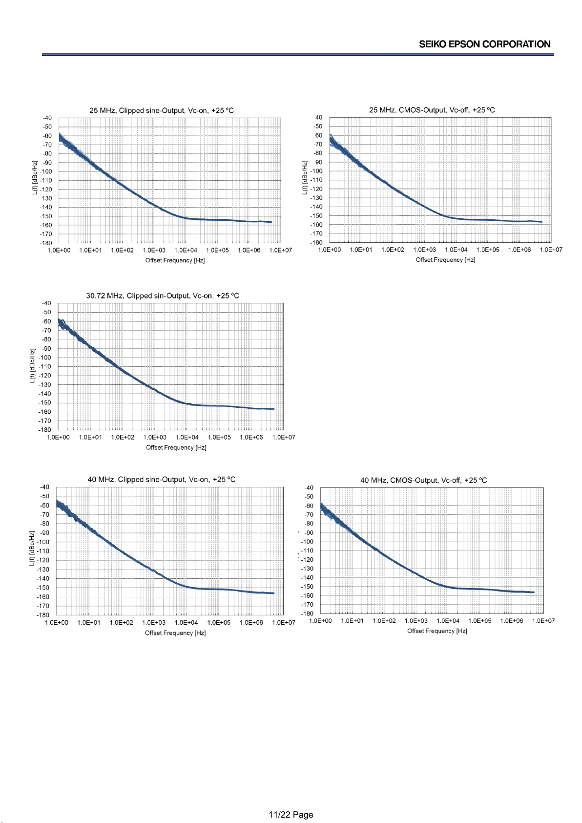
Phase Noise 25 MHz
TCXO mode
() is VC-TCXO mode
L(f)
dBc/Hz
-
-62 (-60)
-
1 Hz offset
-
-93 (-90)
-
10 Hz offset
-
-118 (-116)
-
100 Hz offset
-
-139 (-137)
-
1 kHz offset
-
-153 (-152)
-
10 kHz offset
-
-154 (-154)
-
100 kHz offset
-
-156 (-156)
-
1 MHz offset
Phase Noise 40 MHz
TCXO mode
() is VC-TCXO mode
L(f)
dBc/Hz
-
-59 (-54)
-
1 Hz offset
-
-89 (-83)
-
10 Hz offset
-
-114 (-110)
-
100 Hz offset
-
-135 (-132)
-
1 kHz offset
-
-150 (-149)
-
10 kHz offset
-
-152 (-152)
-
100 kHz offset
-
-155 (-155)
-
1 MHz offset
5) Enable/disable input
Parameter
Symbol
Unit
Min.
Typ.
Max
Notes
Enable voltage
VIH
V
70 % VCC
-
VCC
OE terminal (Enable voltage)
Disable voltage
VIL
V
-
-
30 % VCC
OE terminal (Disable voltage)
Input impedance
-
kΩ
50
-
-
VCC = Typ.
5/22 Page

No.: TG5032xGN_AE_Ver. 1.07
3. Characteristics
3-1) “Frequency / Temperature Characteristics”
3-1-1) Standard spec : ±0.1 × 10⁻⁶ Max. (T_use = -40 °C to +85 °C)
19.2 MHz [N = 40 pcs]
30.72 MHz [N = 40 pcs]
40 MHz [N = 40 pcs]
Temperature [°C]
Temperature [°C]
Temperature [°C]
Temperature [°C]
Temperature [°C]
Temperature [°C]
6/22 Page

No.: TG5032xGN_AE_Ver. 1.07
3-2) Frequency Aging (40 MHz) [N = 5 pcs]
* Aging is estimated from environmental reliability tests and the expected amount of frequency variation over time.
It is not intended as a guarantee of performance over the product-life cycle
3-3) Holdover Stability (19.2 MHz) [N = 40 pcs]
3-4) Frequency Control Characteristics [N = 40 pcs]
7/22 Page

No.: TG5032xGN_AE_Ver. 1.07
3-5) Current Consumption
3-6) Rise time / Fall time (at CMOS output)
3-7) Output voltage [VOH, VOL] (at CMOS output)
3-8) Symmetry (at CMOS output) 3-9) Output level [VPP] (at Clipped sine wave)
8/22 Page

No.: TG5032xGN_AE_Ver. 1.07
3-10) Start up time (19.2 MHz, 40 MHz)
19.2 MHz
40 MHz
9/22 Page

No.: TG5032xGN_AE_Ver. 1.07
3-11) Phase noise (10 MHz, 19.2 MHz, 20 MHz) [N = 25 pcs]
10 MHz
19.2 MHz
20 MHz
10/22 Page
No.: TG5032xGN_AE_Ver. 1.07
3-11) Phase noise (25 MHz, 30.72 MHz, 40 MHz) [n = 25 pcs]
25 MHz
30.72 MHz
40 MHz
11/22 Page
No.: TG5032xGN_AE_Ver. 1.07
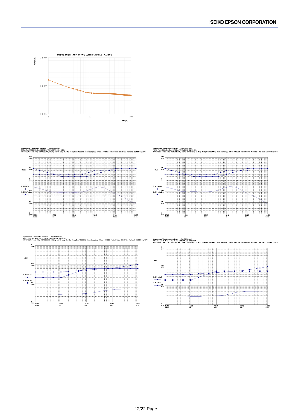
3-12) Short term stability [ADEV] (19.2 MHz) TCXO mode
3-13) TDEV (19.2 MHz, Loop BW = 0.1 Hz)
Constant temperature : +25 °C Constant temperature : +70 °C
3-14) MTIE (19.2 MHz, Loop BW = 0.1 Hz)
Constant temperature : +25 °C Constant temperature : +70 °C
Compliant with G.813 option1 and 2
12/22 Page

No.: TG5032xGN_AE_Ver. 1.07
4. Outline
4-1) Outline dimensions and Pin information
TG5032CGN / SGN
4-2) Soldering pattern
Example of patterning design indicated as follows. In an actual design, please consider mounting density, the reliability of
soldering, etc. and check whether performance is optimal.
Soldering pattern of TG5032CGN / SGN (unit : mm)
Pin
Connections
VC-TCXO
TCXO
1
VC
N.C.
2
N.C.
3
OE
4
GND
5
N.C.
6
OUT
7
N.C.
8
N.C.
9
VCC
10
N.C.
Unit: mm
OE pin = "H" or "open": Specified frequency output.
OE pin = "L" : Output is high impedance.
Do not connect “N.C.” pin with any other leads (also mutually)
If OE Function does not use,
We recommended connecting OE (#3 pin) to VCC (#9 pin)
0.70
1.30
2.50
#1
0.70
1.35
#2
#3 #4
#5
#6
#8
#9
#10
1.35
1.20
#7
1.00
To GND
Please set By-pass capacitor
(0.1μF) near the Vcc pad
To maintain stable operation, provide a 0.1 μF
by-pass capacitor at a location as near as
possible to the power source terminal of the
crystal product (between VCC - GND).
13/22 Page
No.: TG5032xGN_AE_Ver. 1.07
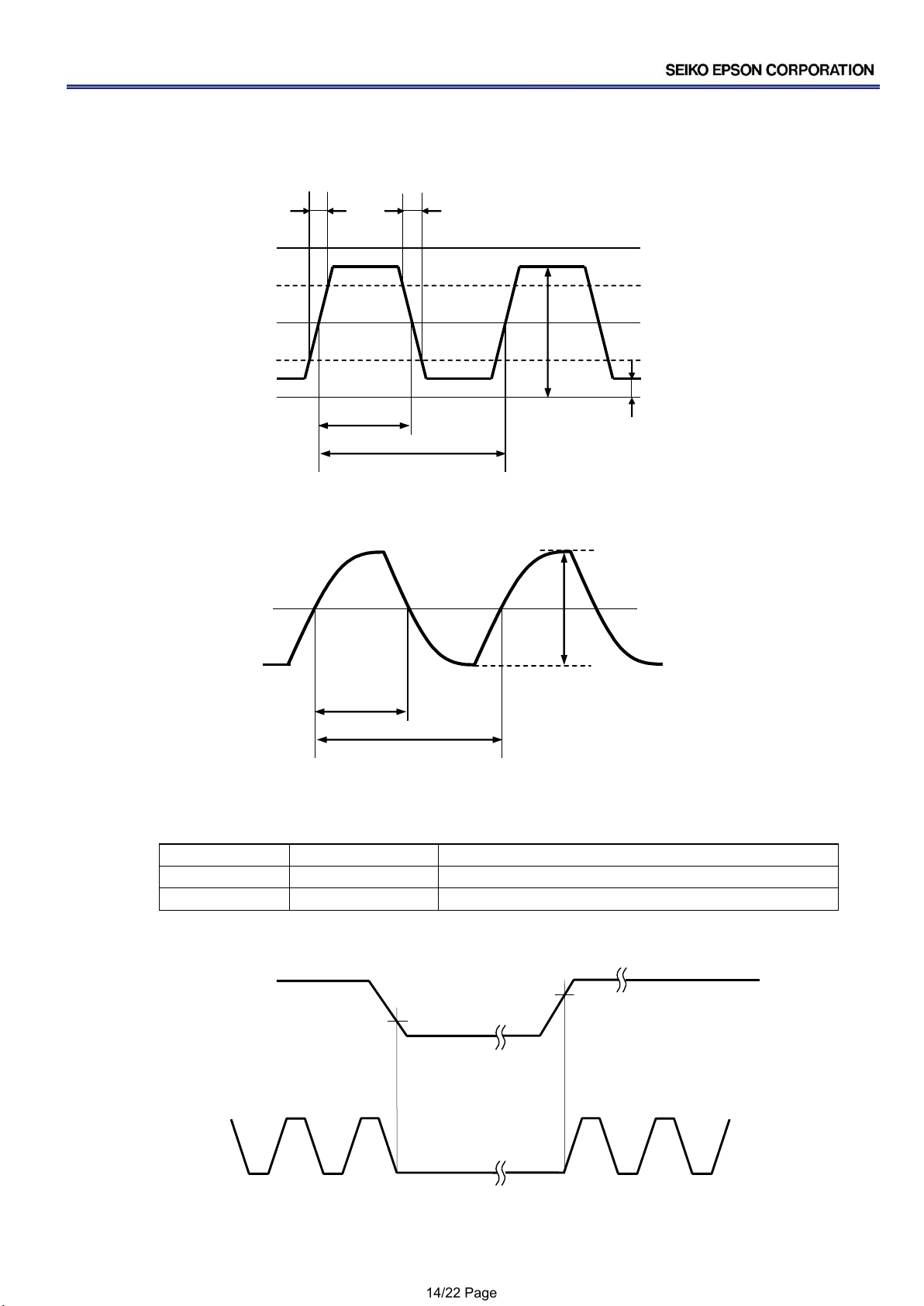
5. Timing chart
5-1-1) Output waveform (CMOS output)
5-1-2) Output waveform (Clipped sine wave output)
5-2) OE function and timing
OE input level
Oscillation
Outputs
“H” or “Open”
Enable
Enable : specified frequency
“L”
Enable
Disable : high impedance
* OE input voltage must be lower than VCC. Note that rise-up time of OE input voltage must not be shorter than
the rise-up time of supply voltage.
VCC
GND
VOL
VOH
tW
t
10 % VCC
50 % VCC
90 % VCC
tr
tf
SYM=tw/t×100 %
GND
Vp-p
tW
t
SYM=tw/t×100 %
high impedance
Enable
Disable
OE
V
IH
V
IL
GND
14/22 Page

No.: TG5032xGN_AE_Ver. 1.07
6. Test circuit
6-1) CMOS output for TCXO
1) Output Load : 15 pF
2) Current consumption
3) Conditions
1. Oscilloscope: Impedance Min. 1 MΩ
Input capacitance Max. 10 pF
Band width Min. 300 MHz
2. Load_C includes probe capacitance.
3. A capacitor (By-pass: 0.1
F) is placed between VCC and GND, and closely to TCXO.
4. Use the current meter whose internal impedance value is small.
5. Power Supply
Impedance of power supply should be as low as possible.
6. GND pin should be connected to low impedance GND.
By-pass
Capacitor
Supply
Voltage
0.1 F
Load_C
15 pF
Test Point
VCC
N.C.
OUT
GND
By-pass
Capacitor
Supply
Voltage
0.1 F
Load_C
15 pF
VCC
N.C.
OUT
GND
A
15/22 Page
No.: TG5032xGN_AE_Ver. 1.07
6-2) CMOS output for VC-TCXO
1) Output Load : 15 pF
2) Current consumption
3) Conditions
1. Oscilloscope: Impedance Min. 1 MΩ
Input capacitance Max. 10 pF
Band width Min. 300 MHz
2. Load_C includes probe capacitance.
3. A capacitor (By-pass: 0.1
F) is placed between VCC and GND, and closely to TCXO.
4. Use the current meter whose internal impedance value is small.
5. Power Supply
Impedance of power supply should be as low as possible.
6. GND pin should be connected to low impedance GND.
By-pass
Capacitor
Supply
Voltage
0.1 F
Load_C
15 pF
Test Point
VCC
Vc
OUT
GND
Control
Voltage
By-pass
Capacitor
Supply
Voltage
0.1 F
Load_C
15 pF
VCC
Vc
OUT
GND
Control
Voltage
A
16/22 Page

No.: TG5032xGN_AE_Ver. 1.07
6-3) Clipped sine wave output for TCXO
1) Output Load : 10 kΩ // 10 pF
2) Current consumption
3) Conditions
1. Oscilloscope: Impedance Min. 1 MΩ
Input capacitance Max. 10 pF
Band width Min. 300 MHz
2. Load_C includes probe capacitance.
3. A capacitor (By-pass: 0.1
F) is placed between VCC and GND, and closely to TCXO.
4. Use the current meter whose internal impedance value is small.
5. Power Supply
Impedance of power supply should be as low as possible.
6. GND pin should be connected to low impedance GND.
Load_C
10 pF
Load_R
10 kΩ
By-pass
Capacitor
Supply
Voltage
Test Point
VCC
N.C.
OUT
GND
0.1 F
DC-cut
Capacitor
0.01 F
Load_C
10 pF
Load_R
10 kΩ
By-pass
Capacitor
VCC
N.C.
OUT
GND
A
Supply
Voltage
0.1 F
DC-cut
Capacitor
0.01 F
17/22 Page
No.: TG5032xGN_AE_Ver. 1.07
6-4) Clipped sine wave output for VC-TCXO
1) Output Load : 10 kΩ // 10 pF
2) Current consumption
3) Conditions
1. Oscilloscope: Impedance Min. 1 MΩ
Input capacitance Max. 10 pF
Band width Min. 300 MHz
2. Load_C includes probe capacitance.
3. A capacitor (By-pass: 0.1
F) is placed between VCC and GND, and closely to TCXO.
4. Use the current meter whose internal impedance value is small.
5. Power Supply
Impedance of power supply should be as low as possible.
6. GND pin should be connected to low impedance GND.
Load_C
10 pF
Load_R
10 kΩ
By-pass
Capacitor
Supply
Voltage
Test Point
VCC
Vc
OUT
GND
Control
Voltage
0.1 F
DC-cut
Capacitor
0.01 F
DC-cut
Capacitor
0.01 F
Load_C
10 pF
Load_R
10 kΩ
By-pass
Capacitor
Supply
Voltage
VCC
Vc.
OUT
GND
Control
Voltage
0.1 F
A
18/22 Page
No.: TG5032xGN_AE_Ver. 1.07
7. Reflow profile (follow to IPC / JEDEC J-STD-020D.1)
8. Packing information
(8-1) Product number last 2 digits code (00) define Quantity. 1 000 pcs/Reel.
TG5032CGN: X1G005231xxxx00 (Please contact Epson for details of number xxxx)
TG5032SGN: X1G005241xxxx00
(8-2) Taping specification Subject to EIA-481 IEC-60286 JIS C0806
(1) Tape dimensions
Material of the Carrier Tape: PS conduct / Material of the Top Tape: PET
(2) Reel dimensions Material of the reel: Conductive polystyrene
Temperature [ C ]
60
300
250
200
150
100
50
0
ts
60 s to 180 s
( +150 C to +200 C )
Avg. Ramp-up
3 C / s Max.
Ramp-down
6 C / s Max.
Time [ s ]
120
180
240
300
360
420
480
540
600
660
720
780
Ts min ; +150 C
Ts max ; +200 C
TL ; +217 C
+255 C
tL
60 s to 150 s
( +217 C over )
tp ; 20 s to 40 s
TP ; +260 C
Time +25 C to Peak
19/22 Page

No.: TG5032xGN_AE_Ver. 1.07
9. Moisture Sensitivity Level, Electro-Static Discharge
(9-1) Moisture Sensitivity Level (MSL)
Parameter
Specifications
Conditions
MSL
LEVEL1
JEDEC J-STD-020D
(9-2) Electro-Static Discharge (ESD)
Parameter
Specifications
Conditions
Human Body Model (HBM)
2 000 V Min
EIAJ ED-4701-1 C111A, 100 pF, 1.5 kΩ, 3 times
Machine Model (MM)
200 V Min
EIAJ ED-4701-1 C111, 200 pF, 0 Ω, 1 time
20/22 Page
This manual suits for next models
1
Table of contents
Other Seiko Epson Power Tools manuals

Popular Power Tools manuals by other brands

Stanley
Stanley 734 AV Series Instruction and service manual

Makita
Makita HM1214C instruction manual

Bosch
Bosch PMF Universal Original instructions

HOLZMANN MASCHINEN
HOLZMANN MASCHINEN BF 16V user manual

Festool
Festool Carvex PS 420 EBQ Original operating manual

OLI
OLI PJ 040 Installation and operating instructions


