SEMIKRON SEMITOP E2 User manual

© by SEMIKRON / 2018-12-03 / Technical Explanation / SEMITOP E2 1200V MLI Inverter Board
PROMGT.1026/ Rev.7/ Template Technical Explanation
Page 1/18
1. Introduction...............................................................................................................................1
1.1 Features ..............................................................................................................................2
1.2 Hardware of the SEMITOP E2 1200V MLI Inverter Board ............................................................2
2. Safety Instructions .....................................................................................................................4
3. Technical Data ...........................................................................................................................6
3.1 Inverter board block diagram..................................................................................................6
3.2 Electrical and mechanical characteristics ..................................................................................6
3.3 Integrated functions ..............................................................................................................9
3.3.1 Gate protection............................................................................................................. 10
3.3.2 VCE,desat diodes .............................................................................................................. 10
3.3.3 Active clamping ............................................................................................................ 10
3.4 Board description ................................................................................................................ 10
3.4.1 Plugs for driver board adaptation ....................................................................................11
3.4.2 Active clamping ............................................................................................................ 11
3.4.3 Plugs for driver board adaptation ....................................................................................12
4. User Interface .......................................................................................................................... 13
4.1 Driver board interface..........................................................................................................13
4.2 DC and AC interface ............................................................................................................ 13
5. Restrictions and Requirements ................................................................................................... 14
5.1 Switching pattern of (T)MLI modules ..................................................................................... 14
5.2 Error treatment................................................................................................................... 14
5.3 Design limits active clamping................................................................................................ 14
5.4 Design limits switching frequency.......................................................................................... 14
5.5 Design limits ambient temperature ........................................................................................ 14
5.6 SEMIKRON assembly ........................................................................................................... 14
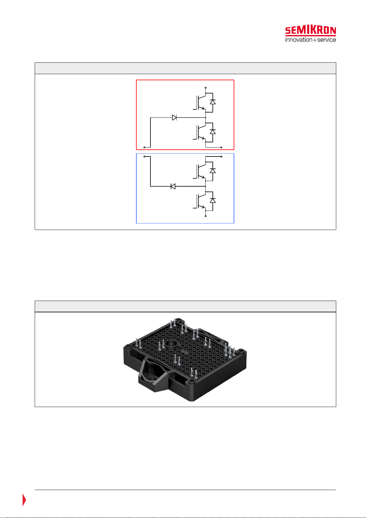
1. Introduction
SEMIKRON set up a 3-phase inverter board for operating SEMITOP E2 1200V MLI modules for evaluation
purposes. The SEMITOP E2 1200V MLI Inverter Board (“inverter board”) is designed to operate with three
SKYPER12 (T)MLI Driver Boards (also a SEMIKRON Application Sample; Technical Explanation available),
one per phase leg. It is designed to operate the module up to a DC-link voltage of 1500V (limited by
insulation coordination) at a maximum switching frequency of 30kHz (limited by insulation coordination);
i.e. higher switching frequencies are possible with a revision of the insulation coordination and the
limitation of the gate driver needs to be taken into account.
Three driver boards (SKYPER 12 (T)MLI Driver Board) are mounted to the inverter board, one per phase
leg (one driver operates switches T1 and T2, the other operates switches T3 and T4). The 1200V MLI phase
leg is split in two SEMITOP E2 module housings, one inheriting switches T1, D1, T2, D2 and D5, the other
housing T3, D3, T4, D4 and D6 (see Figure 1).
The inverter board provides active clamping diodes for all switches and VCE,desat detection diodes for the
outer switches T1 and T4 utilizing the driver boards’ protection functionality. Further all modules have a
built-in NTC sensor (six in total) which are all monitored.
Please read also the Technical Explanation –SKYPER12 (T)MLI Driver Board for detailed information on the
driver boards used together with the inverter board described in this document.
Technical Explanation
SEMITOP E2 1200V
MLI Inverter Board
Revision:
03
Issue date:
2018-12-03
Prepared by:
Ingo Rabl
Reviewed by:
-
Approved by:
Ulrich Nicolai
Keyword: MLI, IGBT driver, inverter, Application Sample, 451375
© by SEMIKRON / 2018-12-03 / Technical Explanation / SEMITOP E2 1200V MLI Inverter Board
PROMGT.1026/ Rev.7/ Template Technical Explanation
Page 2/18
Figure 1: Split MLI in SEMITOP E2
This Application Sample is dedicated to both universities and professional development engineers. It offers
an easy way to set up a three phase inverter with SEMITOP E2 MLI modules and 2L drivers for a DC-link
voltage up to 1500V. Performance tests can be run to prove the possibility of operation at high DC-link
voltages and the high output power.
1.1 Features
The SEMITOP E2 1200V MLI Inverter Board is designed for SK150MLIT12F4TE2 (top half module) and
SK150MLIB12F4TE2 (bottom half module). Both are rated 150A and come with 1200V semiconductors.
Figure 2: SEMITOP E2
Of course all other pin compatible modules can be used as well as long as the design limits are met (e.g.
maximum DC voltage and maximum driver output current may not be exceeded).
1.2 Hardware of the SEMITOP E2 1200V MLI Inverter Board
The SEMITOP E2 1200V MLI Inverter Board consists of a printed circuit board (PCB): it is called “SEMITOP
E2 1200V MLI Inverter Board” with item number 45137501. It provides sockets for three SKYPER12 (T)MLI
Driver Boards, six slots for the power modules (three top half modules and three bottom half modules), DC
and AC terminals.
T1
T2
D1
D2
D5
DC+
N AC
T3
T4
D3
D4
D6
DC-
N AC
MLIT
MLIB
(Top half)
(Bottom half)

© by SEMIKRON / 2018-12-03 / Technical Explanation / SEMITOP E2 1200V MLI Inverter Board
PROMGT.1026/ Rev.7/ Template Technical Explanation
Page 3/18
Figure 3: SKYPER12 (T)MLI Driver Board top view
Depending on the power ratings and the operating conditions (voltage, current, and inductance of the DC-
link connection) it might be necessary to adjust gate resistors, activate or deactivate active clamping
sensing and trip levels of the safety circuits.
The Gerber files of the board are available on request. For ordering the board or the files please contact
your SEMIKRON sales partner.
An appropriate heatsink (and mechanical support for the inverter board) needs to be provided by the user
(see also chapter 3.2).

© by SEMIKRON / 2018-12-03 / Technical Explanation / SEMITOP E2 1200V MLI Inverter Board
PROMGT.1026/ Rev.7/ Template Technical Explanation
Page 4/18
2. Safety Instructions
The SEMITOP E2 1200V MLI Inverter Board bares risks when put in operation. Please carefully read and
obey the following safety instructions to avoid harm or damage to persons or gear.
Table 1: Safety instructions
In operation the SEMITOP E2 1200V MLI
Inverter Board inherits high voltages that are
dangerous to life!
Only qualified personnel should work with the
Kit.
Some parts of the SEMITOP E2 1200V MLI
Inverter Board or connected devices (e.g.
heatsink) may reach high temperatures that
might lead to burns when touched.
When connected to DC-link capacitors it must
be made sure that the DC-link voltage is
reduced to values below 30V before touching
the system.
Insulation coordination and testing has been
performed regarding a PE connection of one
potential. It is mandatory to provide a PE
connection with sufficient cross section when
operating the SEMITOP E2 1200V MLI
Inverter Board.

© by SEMIKRON / 2018-12-03 / Technical Explanation / SEMITOP E2 1200V MLI Inverter Board
PROMGT.1026/ Rev.7/ Template Technical Explanation
Page 5/18
Table 2: Safety regulations for work with electrical equipment
Please follow the safety regulations for working safe with the SEMITOP E2 1200V MLI Inverter Board.
Table 3: No access for people with active implanted cardiac devices!
Operating the Application Sample may go along with electromagnetic fields which may disturb cardiac
devices.
People with cardiac devices shall not operate the device.
Please make sure to always use the appropriate personal safety equipment when working with
the Application Sample.
Safety Regulations
for work with electrical equipment
1) Disconnect mains!
2) Prevent reconnection!
3) Test for absence of harmful voltages!
4) Ground and short circuit!
5) Cover or close of nearby live parts!
To energize, apply in reverse order!
© by SEMIKRON / 2018-12-03 / Technical Explanation / SEMITOP E2 1200V MLI Inverter Board
PROMGT.1026/ Rev.7/ Template Technical Explanation
Page 6/18
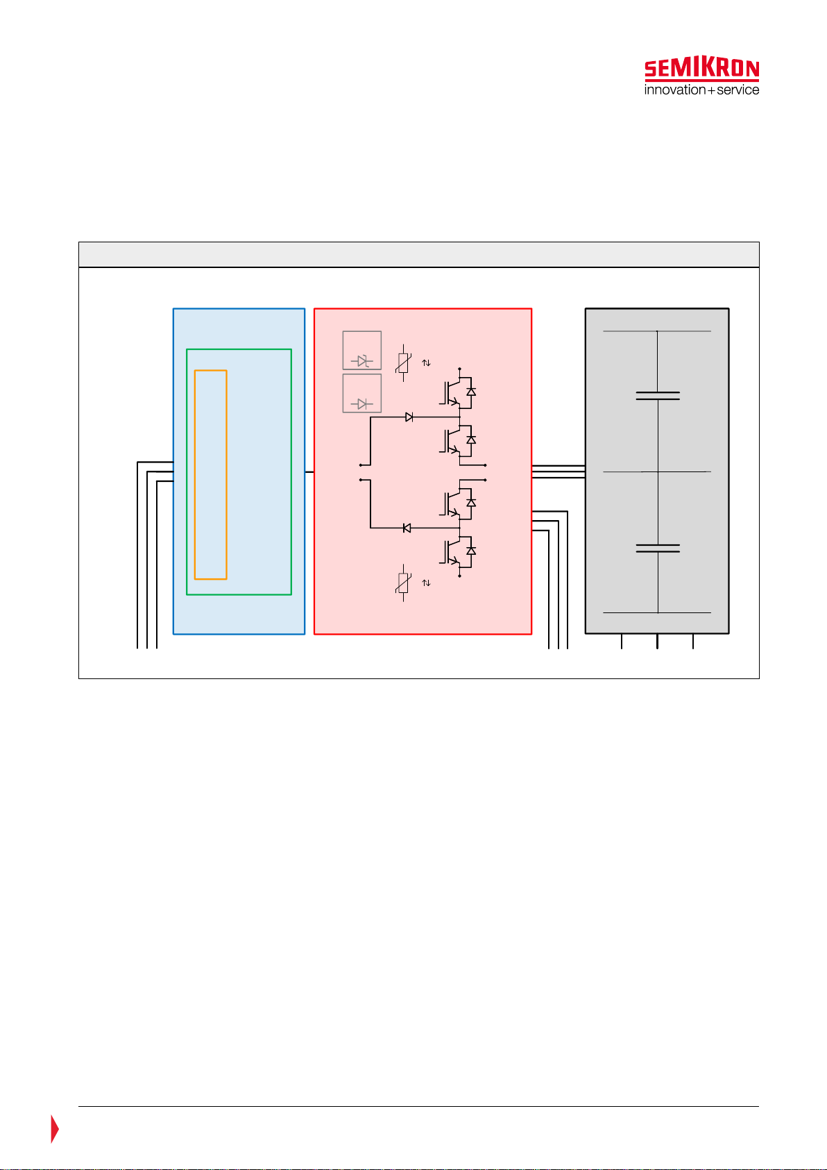
3. Technical Data
3.1 Inverter board block diagram
The electrical block diagram in Figure 4 shows two parts: the blue marked part represents the three driver
boards required to operate the inverter. The red part represents the power modules of the three phase legs
which together with the grey part (the DC-link) forms the SEMITOP E2 1200V MLI Inverter Board.
Figure 4: SEMITOP E2 1200V MLI Inverter Board block diagram
3.2 Electrical and mechanical characteristics
With regard to the requirement specification the SEMITOP E2 1200V MLI Inverter Board allows for
operation within the following boundaries:
-Max. DC-link voltage VDC = 1500V in total, max. 750V per individual DC-link half
-Max. AC voltage VAC = 1000VRMS (line-to-line)
-Ambient temperature Ta= 0°C…40°C (see chapter 5.5 for further information)
-CTI rating of AppS PCBs > 175
Neglecting the above mentioned boundaries may lead to malfunction or damage of the SEMITOP E2 1200V
MLI Inverter Board.
The overall responsibility for a proper insulation coordination remains with the user.
The inverter board is 300mm long and 330mm wide. Including SEMITOP E2 modules the total height is
60mm.
DC+/N/ DC-
3x
SEMITOP E2 1200V MLI Inverter Board
NTC
active
clamping
VCE desat
detection
3x AC
T1
T2
D1
D2
D5
DC+
N AC
T3
T4
D3
D4
D6
DC-
N AC
NTC
SKYPER12 (T)MLI Driver
Board
Interface
DC+
DC-
N
CDC-link
CDC-link
DC-
N
DC+
3x
3x Interface

© by SEMIKRON / 2018-12-03 / Technical Explanation / SEMITOP E2 1200V MLI Inverter Board
PROMGT.1026/ Rev.7/ Template Technical Explanation
Page 7/18
Figure 5: SEMITOP E2 1200V MLI Inverter Board (“inverter board”), top side
Figure 5 shows the top side of the inverter board. Here the diodes for the active clamping circuit are
located.
The SEMITOP E2 power semiconductor modules are mounted on the bottom side of the inverter board
(Figure 6).
330mm
300mm
© by SEMIKRON / 2018-12-03 / Technical Explanation / SEMITOP E2 1200V MLI Inverter Board
PROMGT.1026/ Rev.7/ Template Technical Explanation
Page 8/18
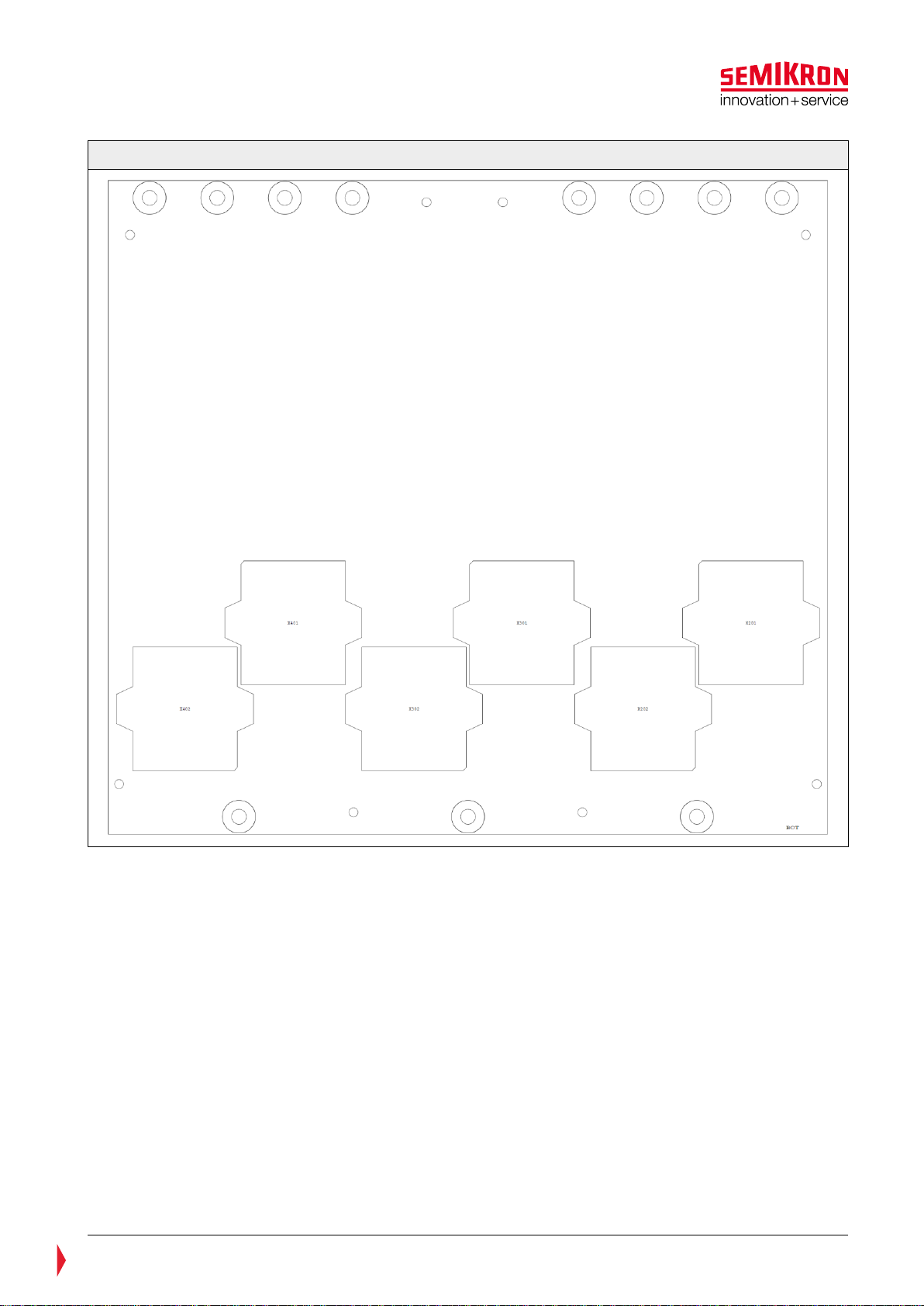
Figure 6: SEMITOP E2 1200V MLI Inverter Board (“inverter board”), bottom side
The user needs to provide a heatsink and a mechanical support for the inverter board. The drill holes that
need to be made are marked in Figure 7. The red circled holes have a diameter of 4.3mm to take M4
supporting posts. The blue circled holes have a diameter of 9mm; through these holes the M4 screws for
mounting the modules can be reached.
The support posts must be able to isolate the DC-link voltage from the heatsink, i.e. no metal posts may be
used.

© by SEMIKRON / 2018-12-03 / Technical Explanation / SEMITOP E2 1200V MLI Inverter Board
PROMGT.1026/ Rev.7/ Template Technical Explanation
Page 9/18
Figure 7: SEMITOP E2 1200V MLI Inverter Board drill holes for mounting
3.3 Integrated functions
The driver board has some optional integrated safety functions to protect the power module from certain
harmful conditions.
© by SEMIKRON / 2018-12-03 / Technical Explanation / SEMITOP E2 1200V MLI Inverter Board
PROMGT.1026/ Rev.7/ Template Technical Explanation
Page 10/18
3.3.1 Gate protection
For gate protection purposes the inverter board is by default equipped with a 10kresistor and a
bidirectional 15V TVS diode between gate and emitter connection of every IGBT. Thus the ESD sensitive
gates are protected even if no driver board is plugged to the inverter board.
3.3.2 VCE,desat diodes
In order to detect desaturation events a diode between collector and the particular driver stage is required.
This diode is located close to each collector on the power board. VCE,desat detection, however, is only
possible, when the driver supports this functionality. SEMIKRON’s SKYPER12 (T)MLI Driver Board supports
desaturation detection.
3.3.3 Active clamping
All required circuitry to provide an operative active clamping protection of the four IGBTs per phase leg is
located on the inverter board. By default the TVS diodes that limit the maximum voltage across each IGBT
are not equipped as the correct value depends on the precise operating conditions (e.g. DC voltage). A
feedback pin from the active clamping to the driver is provided to be able to turn off the output stage of
the driver in order not to work against the active clamping (this functionality is available with the
SKYPER12 (T)MLI Driver Board).
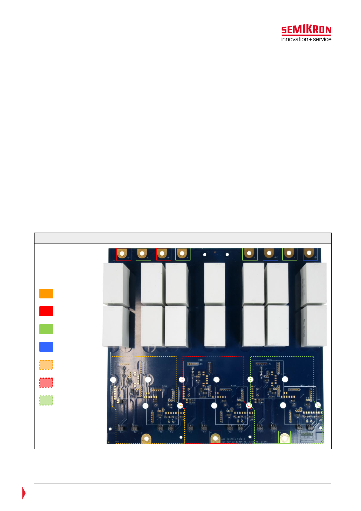
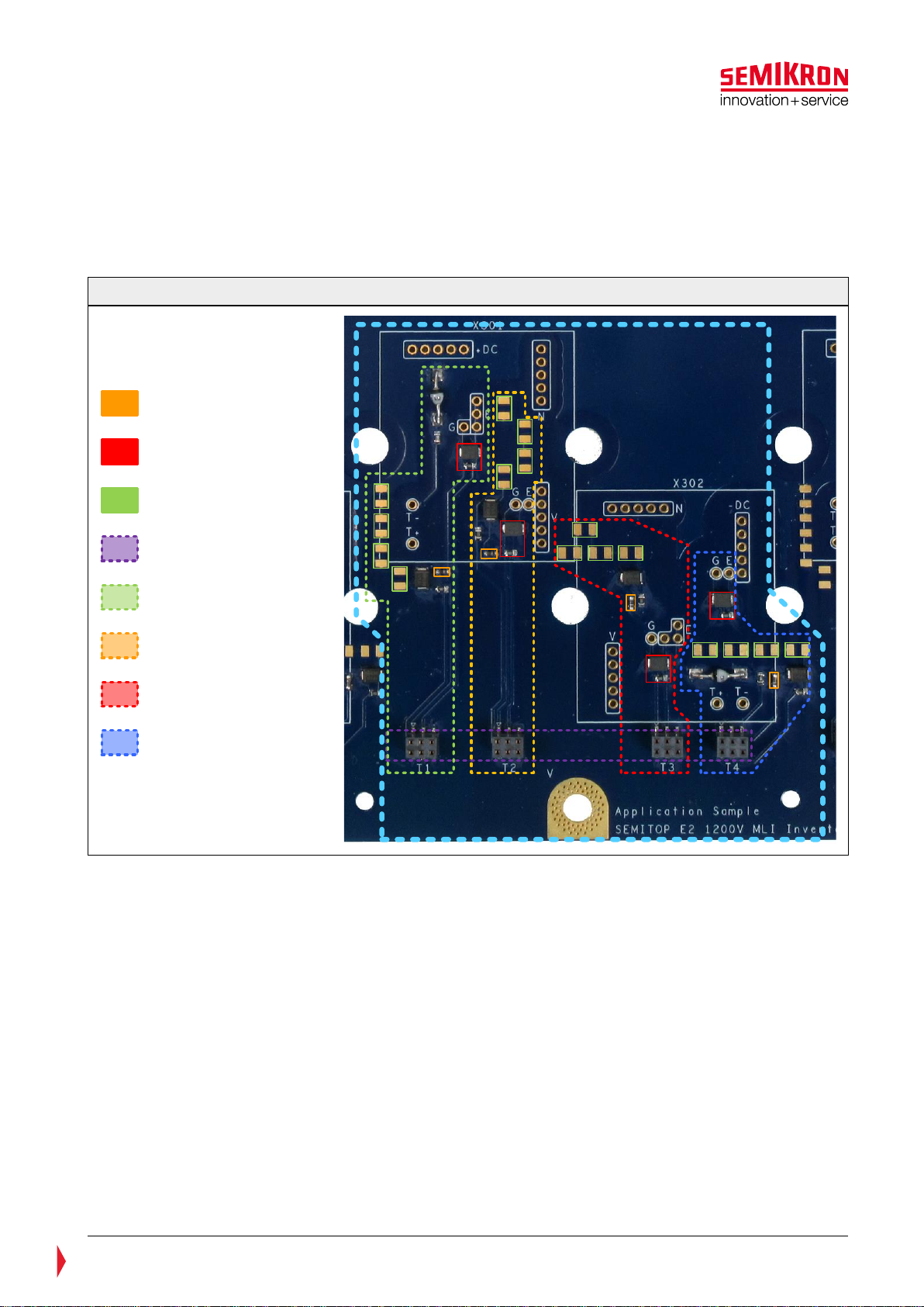
3.4 Board description
Several components are meant to be changed by the user, i.e. an adaptation to the application conditions.
The connections to DC supply and AC output are marked in Figure 8; it also shows three dotted frames
(orange, red and green) which mark three congruent areas (for different phase legs). One of those is
picked exemplarily and explained in detail in Figure 9.
Figure 8: Top side of the inverter board; DC and AC connections
The components that can be changed by the user on the inverter board are marked with different coloured
frames in Figure 8. Figure 9 shows the positions exemplarily at phase V (the light blue dotted frame in
DC+ terminals
Neutral terminals
AC terminals
Circuitry dedicated to phase V
Circuitry dedicated to phase W
Circuitry dedicated to phase U
DC- terminals
© by SEMIKRON / 2018-12-03 / Technical Explanation / SEMITOP E2 1200V MLI Inverter Board
PROMGT.1026/ Rev.7/ Template Technical Explanation
Page 11/18
Figure 9 represents the orange, red and green dotted frames in Figure 8). The positions of all parts are
congruent for phase U, phase V and phase W and only the leading digit in the part number is increased by
one from phase U to phase V and by one from phase V to phase W. Example: X201 ⇒upper half module
phase U; X301 ⇒upper half module phase V, X401 ⇒upper half module phase W.
Figure 9 shows also the position where the SEMIKRON SKYPER12 (T)MLI Driver Board can be plugged to
the inverter board (dotted purple frame).
Function and possible values are explained in chapters 3.4.1 to 3.4.3.
Figure 9: Top side of the driver board; user-changeable components are framed
3.4.1 Plugs for driver board adaptation
The inverter board is designed to be operated with three SKYPER12 (T)MLI Driver Boards (see separate
Technical Explanation for further information [1]). The driver board can be connected to the inverter board
via four 6-pin plugs (framed dotted purple in Figure 9).
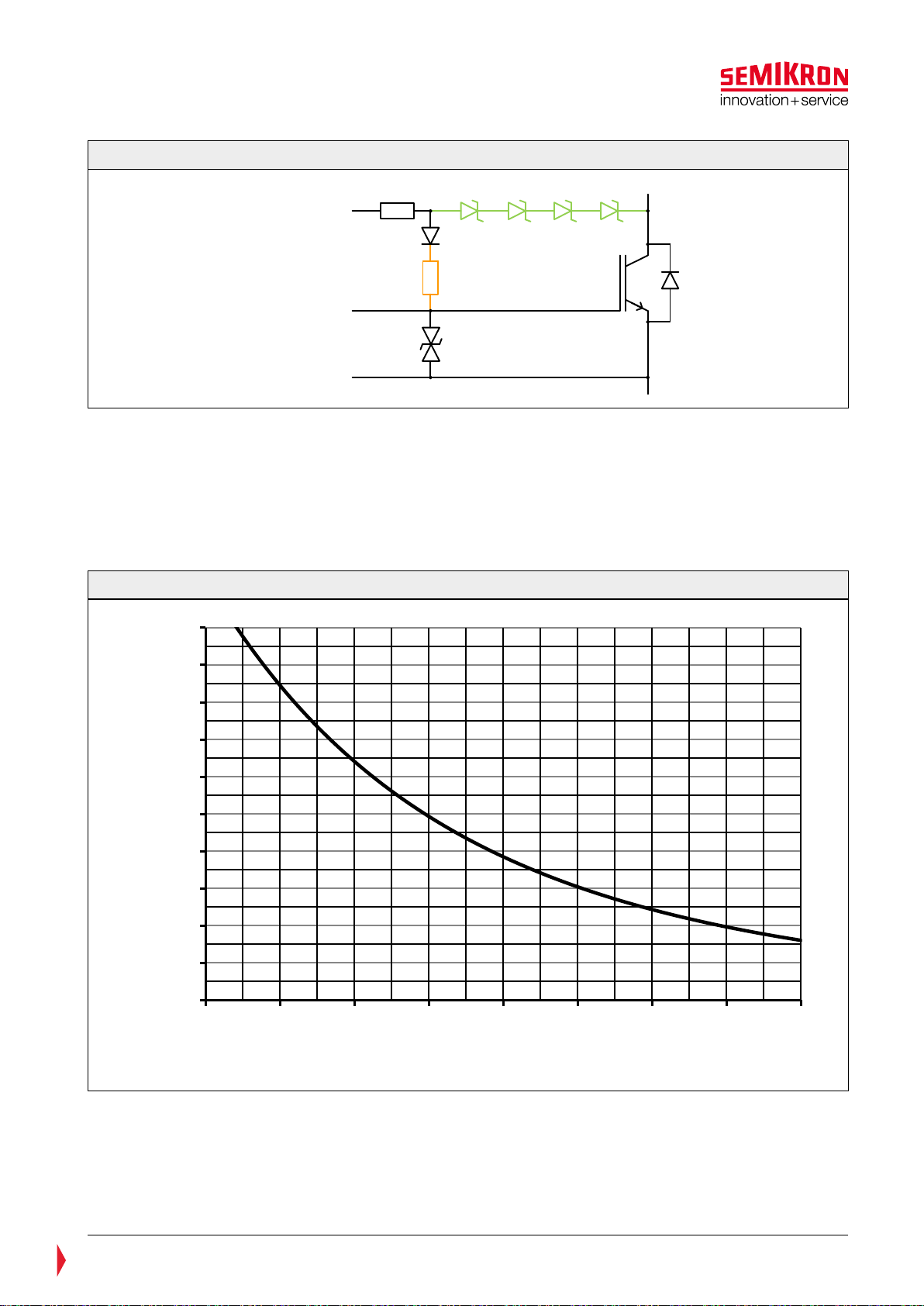
3.4.2 Active clamping
Figure 10 shows the schematic of the active clamping circuit as it is realized on the inverter board. The
orange resistor represents the turn-off resistor which limits the current charging the gate when the active
clamping is in operation. It can be found in Figure 9 framed solid orange. These parts are equipped by
default with 1MiniMELF resistors.
The four SMB sized pads per switch for the TVS diodes (marked green in Figure 10, framed solid green in
Figure 9) are unpopulated by default. If the TVS diodes are not installed (no active clamping functionality)
it is necessary to deactivate the clamp sensing input of the SKYPER12 (T)MLI Driver Board if it is in use
with the inverter board (see also [1]).
G-E SMB-size suppressor diode
G-E resistor
Pads for 4x SMB-size TVS diodes for
active clamping
Plugs for driver board
1x MiniMELF / 1206 pads for active
clamping turn-off resistor
X303
X304
X305
X306
Circuitry dedicated to T1
Circuitry dedicated to T3
Circuitry dedicated to T4
Circuitry dedicated to T2
© by SEMIKRON / 2018-12-03 / Technical Explanation / SEMITOP E2 1200V MLI Inverter Board
PROMGT.1026/ Rev.7/ Template Technical Explanation
Page 12/18
Figure 10: Schematic of active clamping
Please refer to chapter 5.3 for further information.
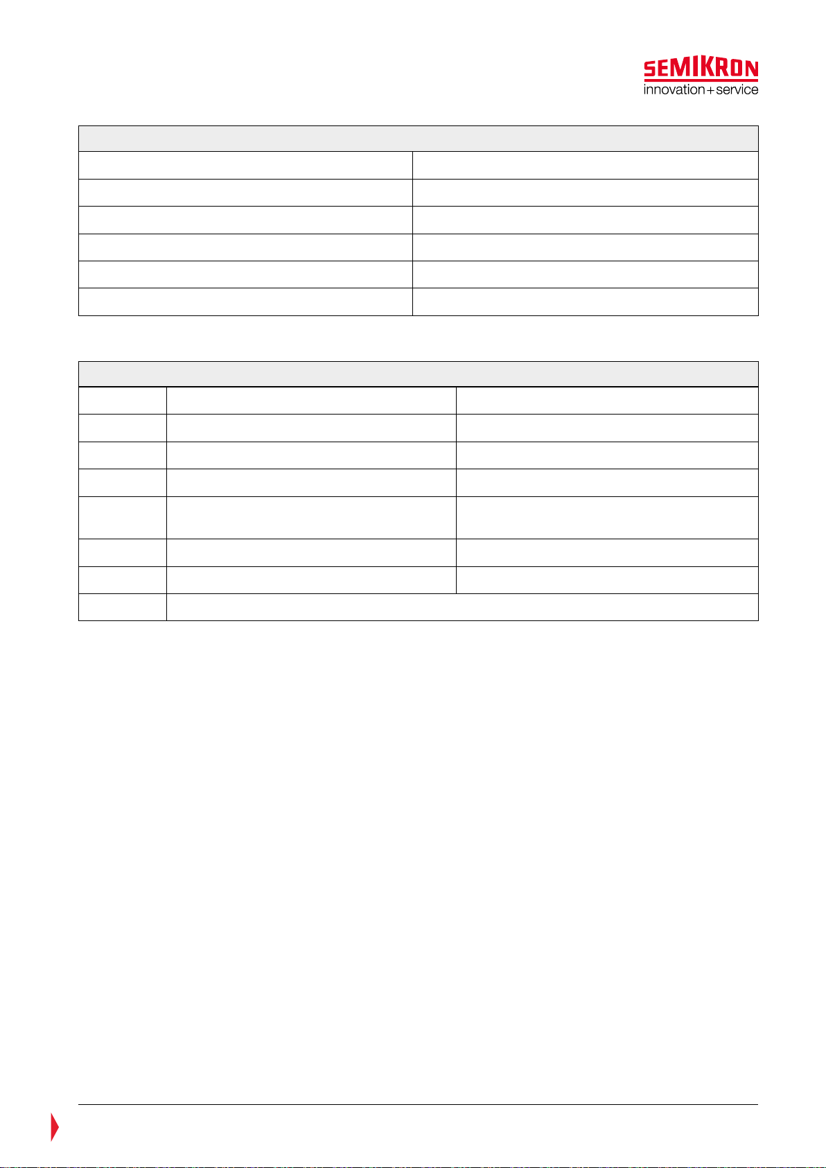
3.4.3 Plugs for driver board adaptation
The SEMITOP E2 modules that can be operated with the inverter board have a built-in NTC temperature
sensor. Figure 11 shows an excerpt of the NTC characteristic which includes the most interesting
temperature range between 70°C and 150°C. The full characteristic can be found in the Technical
Explanations of SEMITOP E or can be calculated from the formula given in the SEMITOP E2 datasheets [1].
Figure 11: SEMITOP E2 NTC characteristic (excerpt)
to clamp sensing
input of SKYPER 12
(T)MLI Driver Board
connected to gate
driver output
TVS diodes
suppressor diode for
gate protection
100k
Active clamping
turn-off resistor
1R
0
100
200
300
400
500
600
700
800
900
1000
70 80 90 100 110 120 130 140 150
[]
[°C]

© by SEMIKRON / 2018-12-03 / Technical Explanation / SEMITOP E2 1200V MLI Inverter Board
PROMGT.1026/ Rev.7/ Template Technical Explanation
Page 13/18
4. User Interface
4.1 Driver board interface
The connection between inverter board and driver board is established by X203, X204, X205 and X206 for
phase U, X303, X304, X305 and X306 for phase V and X403, X404, X405 and X406 for phase W.
Plugs Xxx3and Xxx6show the same pinout as well as plugs Xxx4and Xxx5. The pinouts are explained in
Table 4 and Table 5.
Table 4: Xxx3 (Xxx6) on inverter board interface to driver board
Pin
Description
1
Gate potential of T1 (T4)
2
Active Clamping sense of T1 (T4)
3
Emitter potential of T1 (T4)
4
Pin T+ of SEMITOP E2 module’s NTC sensor T1 (T4)
5
VCE,desat detection of T1 (T4)
6
Pin T- of SEMITOP E2 module’s NTC sensor T1 (T4)
Table 5: Xxx4 (Xxx5) on inverter board interface to driver board
Pin
Description
1
Gate potential of T2 (T3)
2
Active Clamping sense of T2 (T3)
3
Emitter potential of T2 (T3)
4
not connected
5
VCE,desat detection of T2 (T3)
6
not connected
4.2 DC and AC interface
The DC and AC interfaces are realized by PCB contact areas where cable shoes can be directly mounted by
using an M6 screw. A washer with the same size as the PCB contact area allows for a planar contact
between cable shoe and inverter board.
The cable shoes may not exceed the size of the DC contact areas in order not to reduce insulation
distances.

© by SEMIKRON / 2018-12-03 / Technical Explanation / SEMITOP E2 1200V MLI Inverter Board
PROMGT.1026/ Rev.7/ Template Technical Explanation
Page 14/18
5. Restrictions and Requirements
This chapter claims some restrictions that must be paid attention to in order to avoid damage to inverter
board or power semiconductor.
5.1 Switching pattern of (T)MLI modules
A detailed explanation of the MLI switching pattern is given in the SEMIKRON Application Note AN-11001
[3]. Summed up always an inner IGBT (T2 or T3) must be switched on first, the corresponding outer IGBT
(T1 or T4) after a short while, namely when the inner IGBT is entirely switched on. For switch-off this
sequence must be maintained in reverse order: it must be made sure that T1 (T4) is thoroughly turned off
before T2 (T3) may be switched off.
This sequence is recommended to be maintained at any time, even and especially in case of
emergency shut-down (e.g. because of over current or desaturation).
5.2 Error treatment
The inverter board provides active clamping functionality only. In case desaturation events or thermal
overloads take place, the connected driver needs to react accordingly. All required functionality for an
extensive error management is integrated in the SKYPER12 (T)MLI Driver Board. SEMIKRON recommends
using this driver board for proper and save operation.
If other driving equipment shall be used it must be made sure that the aforementioned events are treated
correctly.
5.3 Design limits active clamping
The clamping voltage for protecting the IGBTs can be adjusted by changing the breakdown voltage of the
TVS diodes.
SEMIKRON recommends to use four diodes with the same breakdown voltage. Using less diodes and 0
jumpers instead or using diodes with different breakdown voltages influences the blocking voltage sharing
across the individual pads. This might influence the overall insulation capability. Therefore the insulation
capability needs to be checked in case this approach is desired.
The total breakdown voltage (sum of the breakdown voltages of all TVS diodes) must under all
circumstances (tolerances of the breakdown voltage, thermal drift) be lower than the breakdown voltage of
the IGBT that shall be protected.
On the other hand the clamping shall not work when just the maximum DC-link voltage is applied and the
inverter is operating in normal operation (i.e. maximum DC-link voltage plus voltage overshoot in normal
operation) in order not to increase the switching losses.
5.4 Design limits switching frequency
The maximum switching frequency is determined by the used modules and their gate charge and the power
of the drivers. It is limited to 30kHz by insulation coordination. Further information on calculating the
switching frequency limit can be found in Application Note AN-7004 [5].
5.5 Design limits ambient temperature
This Application Sample has been developed as reference design for laboratory use and tested up to 40°C
accordingly.
However, it might be possible to extend the ambient temperature range; the responsibility to test and
qualify this larger range remains with the user.
5.6 SEMIKRON assembly
SEMIKRON has tested the Application Sample with three SKYPER12 (T)MLI Driver Boards utilizing not
optimized forced air cooled heatsink. All results shown are valid for the particular revisions shown in Table
6 only.
© by SEMIKRON / 2018-12-03 / Technical Explanation / SEMITOP E2 1200V MLI Inverter Board
PROMGT.1026/ Rev.7/ Template Technical Explanation
Page 15/18
Table 6: Part revisions for SEMIKRON tests
Part
Revision
SEMITOP E2 1200V MLI Inverter Board
45137501_04
SKYPER 12
L5069901
SKYPER12 (T)MLI Driver Board
45137601_02
SK150MLIT12F4TE2
Datecode: 17010P R
SK150MLIB12F4TE2
Datecode: 17010P R
Variable part values have been chosen according to Table 7.
Table 7: Part values for SEMIKRON tests
Part
Resulting value for T1 and T4
Resulting value for T2 and T3
RGon
1.65
1.65
RGoff
1.65
1.65
RSoft
5.1
5.1
Active
Clamping
4x 170V (i.e. four TVS diodes with a
nominal breakdown voltage of 170V)
4x 170V (i.e. four TVS diodes with a nominal
breakdown voltage of 170V)
RCE
7.5k
n.c.
CCE
820pF
820pF
Rtemp,threshold
With the above mentioned values an absolute maximum operation up to 1500VDC and 75ARMS is possible at
all power factor values at a maximum ambient temperature of 40°C.
It can also withstand soft and hard short circuits, when the active clamping circuits are adjusted to come
into action at VCE=1000..1100V.
The SEMITOP E2 1200V MLI Inverter Board has passed isolation and partial discharge tests.
It is up to the customer to optimize user-changeable values according to the particular operation and do
the necessary tests with these changes.

© by SEMIKRON / 2018-12-03 / Technical Explanation / SEMITOP E2 1200V MLI Inverter Board
PROMGT.1026/ Rev.7/ Template Technical Explanation
Page 16/18
Figure 1: Split MLI in SEMITOP E2 .....................................................................................................2
Figure 2: SEMITOP E2 ......................................................................................................................2
Figure 3: SKYPER12 (T)MLI Driver Board top view ...............................................................................3
Figure 4: SEMITOP E2 1200V MLI Inverter Board block diagram ............................................................6
Figure 5: SEMITOP E2 1200V MLI Inverter Board (“inverter board”), top side..........................................7
Figure 6: SEMITOP E2 1200V MLI Inverter Board (“inverter board”), bottom side ....................................8
Figure 7: SEMITOP E2 1200V MLI Inverter Board drill holes for mounting ...............................................9
Figure 8: Top side of the inverter board; DC and AC connections ......................................................... 10
Figure 9: Top side of the driver board; user-changeable components are framed................................... 11
Figure 10: Schematic of active clamping........................................................................................... 12
Figure 11: SEMITOP E2 NTC characteristic (excerpt) ..........................................................................12
Table 1: Safety instructions ..............................................................................................................4
Table 2: Safety regulations for work with electrical equipment ..............................................................5
Table 3: No access for people with active implanted cardiac devices! .....................................................5
Table 4: Xxx3 (Xxx6) on inverter board interface to driver board......................................................... 13
Table 5: Xxx4 (Xxx5) on inverter board interface to driver board......................................................... 13
Table 6: Part revisions for SEMIKRON tests....................................................................................... 15
Table 7: Part values for SEMIKRON tests .......................................................................................... 15

© by SEMIKRON / 2018-12-03 / Technical Explanation / SEMITOP E2 1200V MLI Inverter Board
PROMGT.1026/ Rev.7/ Template Technical Explanation
Page 17/18
Symbols and Terms
Letter Symbol
Term
3L
Three level
DC-
Negative potential (terminal) of a direct voltage source
DC+
Positive potential (terminal) of a direct voltage source
fsw
Switching frequency
GND
Ground
IGBT
Insulated Gate Bipolar Transistor
N
Neutral potential (terminal) of a direct voltage source; midpoint between DC+
and DC-
n.c.
not connected
NTC
Temperature sensor with negative temperature coefficient
PELV
Protective Extra Low Voltage
PWM
Pulse Width Modulation
RGint
Internal gate resistance
RGoff
External gate series resistor at switch-off
RGon
External gate series resistor at switch-on
RMS
Root Mean Square
SELV
Safety Extra Low Voltage
Ta
Ambient temperature
Tj
Junction temperature
TNPC
T-type Neutral Point Clamped
TVS
Transient voltage suppressor
VCE
Collector-emitter voltage
VDC
Total supply voltage between DC+ and DC-
A detailed explanation of the terms and symbols can be found in the "Application Manual Power
Semiconductors" [2]
References
[1] www.SEMIKRON.com
[2] A. Wintrich, U. Nicolai, W. Tursky, T. Reimann, “Application Manual Power Semiconductors”, 2nd
edition, ISLE Verlag 2015, ISBN 978-3-938843-83-3
[3] I. Staudt, “3L NPC & TNPC Topology”, SEMIKRON Application Note, AN-11001 - rev05, 2015
[4] M. Hermwille, “Gate Resistor – Principles and Applications”, SEMIKRON Application Note, AN-7003 -
rev00, 2007
[5] M. Hermwille, “IGBT Driver Calculation”, SEMIKRON Application Note, AN-7004 - rev00, 2007
[6] J. Krapp, “Technical Explanation SKYPER®12 –rev5”, SEMIKRON Technical Explanation, 2017
[7] R. Agostini, “Technical Explanation SEMITOP®–rev5”, SEMIKRON Technical Explanation, 2017

© by SEMIKRON / 2018-12-03 / Technical Explanation / SEMITOP E2 1200V MLI Inverter Board
PROMGT.1026/ Rev.7/ Template Technical Explanation
Page 18/18
IMPORTANT INFORMATION AND WARNINGS
The information in this document may not be considered as guarantee or assurance of product characteristics
("Beschaffenheitsgarantie"). This document describes only the usual characteristics of products to be expected in typical
applications, which may still vary depending on the specific application. Therefore, products must be tested for the
respective application in advance. Application adjustments may be necessary. The user of SEMIKRON products is
responsible for the safety of their applications embedding SEMIKRON products and must take adequate safety measures
to prevent the applications from causing a physical injury, fire or other problem if any of SEMIKRON products become
faulty. The user is responsible to make sure that the application design is compliant with all applicable laws, regulations,
norms and standards. Except as otherwise explicitly approved by SEMIKRON in a written document signed by authorized
representatives of SEMIKRON, SEMIKRON products may not be used in any applications where a failure of the product or
any consequences of the use thereof can reasonably be expected to result in personal injury. No representation or
warranty is given and no liability is assumed with respect to the accuracy, completeness and/or use of any information
herein, including without limitation, warranties of non-infringement of intellectual property rights of any third party.
SEMIKRON does not assume any liability arising out of the applications or use of any product; neither does it convey any
license under its patent rights, copyrights, trade secrets or other intellectual property rights, nor the rights of others.
SEMIKRON makes no representation or warranty of non-infringement or alleged non-infringement of intellectual property
rights of any third party which may arise from applications. This document supersedes and replaces all information
previously supplied and may be superseded by updates. SEMIKRON reserves the right to make changes.
SEMIKRON INTERNATIONAL GmbH
Sigmundstrasse 200, 90431 Nuremberg, Germany
Tel: +49 911 6559 6663, Fax: +49 911 6559 262
sales@semikron.com, www.semikron.com
Table of contents
Other SEMIKRON DC Drive manuals


