Seneca T201DCH50-MU User manual

ORIGINAL INSTRUCTIONS
USER MANUAL
T201DCH50-MU
T201DCH100-MU
T201DCH300-MU
AC/DC TRUE RMS or DC BIPOLAR CURRENT TRANSFORMER
WITH MODBUS RTU PROTOCOL AND ANALOG/DIGITAL OUTPUT
SENECA S.r.l.
Via Austria 26 –35127 –Z.I. - PADOVA (PD) - ITALY
Tel. +39.049.8705355 –8705355 Fax +39 049.8706287
www.seneca.it

User Manual
T201DCH50/100/300-MU
ALL RIGHTS RESERVED. NO PART OF THIS PUBLICATION MAY
BE REPRODUCED WITHOUT PRIOR PERMISSION.
www.seneca.it
Doc. MI00546-EN
Rev. 1.0.0.0
Page 2
Introduction
Contents of the present documentation refer to products and technologies described in it.
All technical data contained in the document may be modified without prior notice.
Content of this documentation is subject to periodical revision.
To use the product safely and effectively, read carefully the following instructions before use.
The product must be used only for the use for which it was designed and built: any other use must be
considered with full responsibility of the user.
The installation, programming and set-up is allowed only to authorized operators, physically and intellectually
suitable.
Set up shall be performed only after a correct installation and the user shall perform every operation described
in the installation manual carefully.
Seneca is not considered liable for failure, breakdown, accident caused because of ignorance or failure to
apply the indicated requirements.
Seneca is not considered liable for any unauthorized changes.
Seneca reserves the right to modify the device, for any commercial or construction requirements, without the
obligation to promptly update the reference manuals.
No liability for the contents of this documents can be accepted.
Use the concepts, examples and other content at your own risk.
There may be errors and inaccuracies in this document that may of course be damaging to your system.
Proceed with caution, and although this is highly unlikely, the author(s) do not take any responsibility for that.
Technical features subject to change without notice.
CONTACT US
Technical support
Product information
Document revisions
DATE
REVISION
NOTES
20/02/2019
1.0.0.0
First Revision
This document is property of SENECA srl. Duplication and reproduction are forbidden, if not authorized.

User Manual
T201DCH50/100/300-MU
ALL RIGHTS RESERVED. NO PART OF THIS PUBLICATION MAY
BE REPRODUCED WITHOUT PRIOR PERMISSION.
www.seneca.it
Doc. MI00546-EN
Rev. 1.0.0.0
Page 3
TABLE OF CONTENTS
DEVICE DESCRIPTION AND INTENDED USE...........................................................4
1.1. Description ..............................................................................................................................................................................4
1.2. Features ...................................................................................................................................................................................4
CONFIGURING THE DEVICE ......................................................................................5
DIP SWITCH CONFIGURATION..................................................................................6
3.1. Loading configuration from flash..........................................................................................................................................6
3.2. Setting the RS485 Modbus RTU Station Address................................................................................................................6
3.3. Setting the RS485 Baud rate ..................................................................................................................................................7
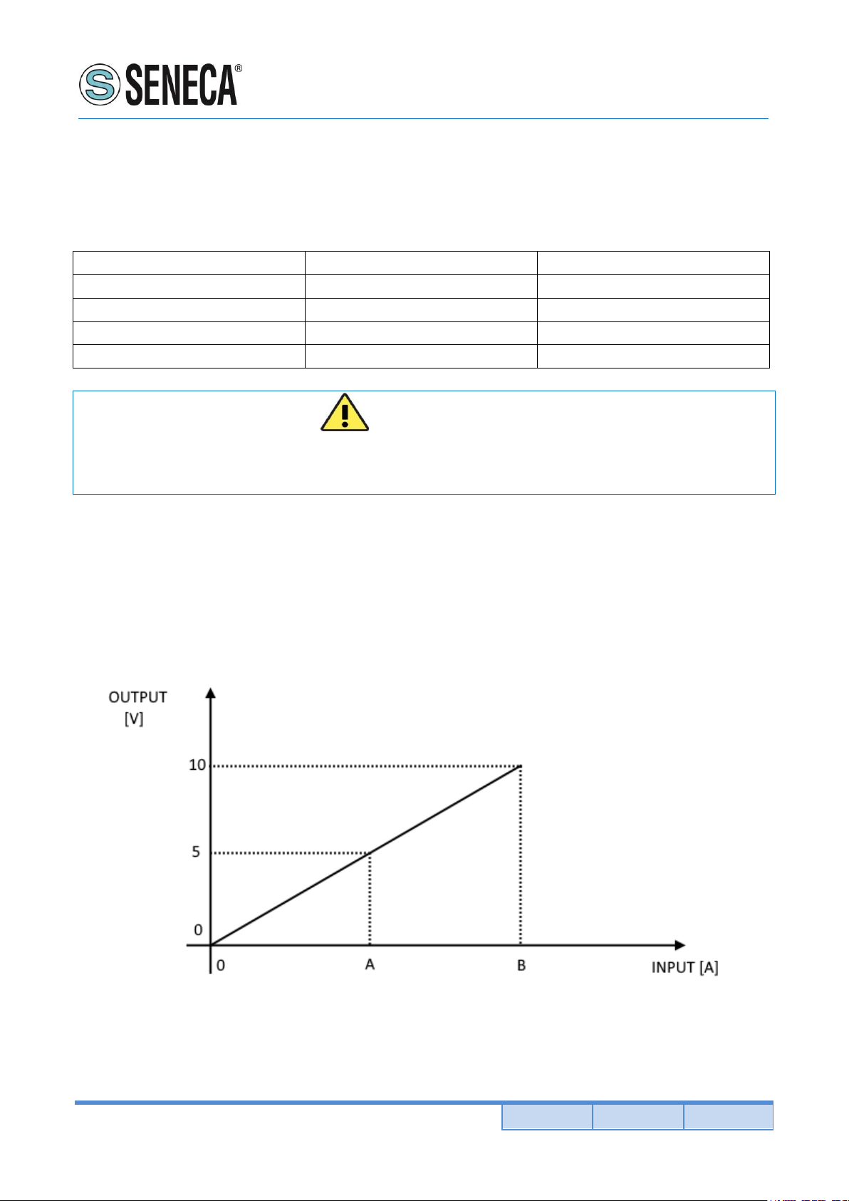
3.4. Setting the RMS/Bipolar mode and 50% - 100% full scale ..................................................................................................7
MODBUS RTU PROTOCOL.........................................................................................9
4.1. Modbus RTU function code supported.................................................................................................................................9
MODBUS REGISTER TABLE....................................................................................10
5.1. "0-BASED" OR "1-BASED” MODBUS ADDRESSES ..........................................................................................................10
5.1.1. MODBUS ADDRESSES WITH "0-BASED" CONVENTION..........................................................................................12
5.1.2. MODBUS ADDRESSES WITH "1 BASED" CONVENTION (STANDARD)...................................................................12
5.2. BIT CONVENTION WITHIN A MODBUS HOLDING REGISTER ..........................................................................................13
5.3. MSB and LSB BYTE CONVENTION WITHIN A MODBUS HOLDING REGISTER..............................................................13
5.4. REPRESENTATION OF A 32-BIT VALUE IN TWO CONSECUTIVE MODBUS HOLDING REGISTERS ...........................13
5.5. TYPE OF 32-BIT FLOATING POINT DATA (IEEE 754) ........................................................................................................14
5.6. T201DCH-MU: MODBUS 4xxxx HOLDING REGISTERS TABLE (FUNCTION CODE 3)....................................................15
FULL CONFIGURATION WITH EASY SETUP..........................................................19
6.1. Easy Setup Menu ..................................................................................................................................................................19
6.2. Creating a Project Configuration.........................................................................................................................................20
6.3. Testing the Device ................................................................................................................................................................23
6.3.1. The datalogger ..............................................................................................................................................................24

User Manual
T201DCH50/100/300-MU
ALL RIGHTS RESERVED. NO PART OF THIS PUBLICATION MAY
BE REPRODUCED WITHOUT PRIOR PERMISSION.
www.seneca.it
Doc. MI00546-EN
Rev. 1.0.0.0
Page 4
DEVICE DESCRIPTION AND INTENDED USE
WARNING!
This User Manual extend the information from the Installation Manual about the device configuration.
Use the Installation Manual for more info.
WARNING!
Under any circumstances, SENECA s.r.l. or its suppliers shall not be responsible for loss of recording
data/incomes or for consequential or incidental damage due to neglect or reckless mishandling of the
device, even though SENECA is well aware of these possible damages.
SENECA, its subsidiaries, affiliates, companies of the group, its suppliers and retailers shall not
guarantee that the functions will satisfy completely customer’s expectations or that device, the
firmware and the software shall have no errors or work continuously.
1.1. Description
The T201DCH50/100/300-MU are isolated, contact less loop powered AC/DC current transducers. The look
and device’s function are very similar to those of an active standard Current Transformer, but with the
remarkable feature of measuring the DC and AC component. For its electrical endurance, ease of use and
compact dimensions, the T201DCH50-MU, T201DCH100-MU and T201DCH300-MU fit every kind of current
measurement: up to 50 Adc/Aac, 100 Adc/Aac and 300 Adc/Aac (respectively).
A RS485 port and an USB port with a standard Modus RTU slave protocol are also available.
The device can measure a current in 2 different modes (using dip switches or the Easy Setup Software):
TRUE RMS AC/DC CURRENT MEASURE
DC BIPOLAR CURRENT MEASURE (used also for obtain the sign +/- of a DC current)
1.2. Features
Similar usage to a standard alternating current active C.T.
No shunt, no wasted power from the measure circuit
High accuracy rating
Analog 0/10V dc with configurable start/stop values
Digital Output configurable Alarm (Max, Min, Window)
Suitable for use with all Seneca modules that allow to power the device with at least 12 Vdc and having a
0 –10Vdc input
Simple configurable with dip switches or with the free Easy Setup software
Two ranges, dip-switch selectable

User Manual
T201DCH50/100/300-MU
ALL RIGHTS RESERVED. NO PART OF THIS PUBLICATION MAY
BE REPRODUCED WITHOUT PRIOR PERMISSION.
www.seneca.it
Doc. MI00546-EN
Rev. 1.0.0.0
Page 5
Damping filter availability to improve stable reading
Modbus RTU protocol by RS485 and USB ports
Modbus Address/Baud Rate/Range/Mode configurable also from dip switch
Suitable for batteries, battery chargers, solar panels, power units and generic dc and ac loads.
Compact size: overall dimensions less than 96,5 x 68 x 26 mm
Baud rate for Modbus RTU: from 1200 baud up to 115200 baud
Start/Stop Input/Output Alarm Values configurable with Easy Setup software
I Max/Min Resettable by Modbus RTU registers
Quick installation on DIN 46277 rail
Refer to the installation manual for more information.
CONFIGURING THE DEVICE
The Device can be configured in two ways:
A basic configuration from dip switches
A full configuration from flash (using Easy Setup Software by the USB port)
WARNING!
Dip switches configuration are active only after a reboot!
WARNING!
The Dip Switch setting will overwrite the Flash setting so, if you need to use the flash configuration
you MUST set ALL dip switches to “OFF”.

User Manual
T201DCH50/100/300-MU
ALL RIGHTS RESERVED. NO PART OF THIS PUBLICATION MAY
BE REPRODUCED WITHOUT PRIOR PERMISSION.
www.seneca.it
Doc. MI00546-EN
Rev. 1.0.0.0
Page 6
DIP SWITCH CONFIGURATION
3.1. Loading configuration from flash
If ALL Dip Switch 1…8 are OFF, the device use the Flash configuration (you must use the Easy Setup
Software for configure)
Load
Configuration
DIP1
DIP2
DIP3
DIP4
DIP5
DIP6
DIP7
DIP8
FROM FLASH
OFF
OFF
OFF
OFF
OFF
OFF
OFF
OFF
3.2. Setting the RS485 Modbus RTU Station Address
Dip Switch 1..4 are using for configure the Modbus RTU Station Address:
Modbus RTU
Address
DIP1
DIP2
DIP3
DIP4
1
ON
OFF
OFF
OFF
2
OFF
ON
OFF
OFF
3
ON
ON
OFF
OFF
4
OFF
OFF
ON
OFF
5
ON
OFF
ON
OFF
6
OFF
ON
ON
OFF
7
ON
ON
ON
OFF
8
OFF
OFF
OFF
ON
9
ON
OFF
OFF
ON
10
OFF
ON
OFF
ON
11
ON
ON
OFF
ON
12
OFF
OFF
ON
ON
13
ON
OFF
ON
ON
14
OFF
ON
ON
ON
15
ON
ON
ON
ON

User Manual
T201DCH50/100/300-MU
ALL RIGHTS RESERVED. NO PART OF THIS PUBLICATION MAY
BE REPRODUCED WITHOUT PRIOR PERMISSION.
www.seneca.it
Doc. MI00546-EN
Rev. 1.0.0.0
Page 7
3.3. Setting the RS485 Baud rate
Dip Switch 5..6 are used for setting the Baud Rate
Baud Rate
DIP5
DIP6
9600
OFF
OFF
19200
ON
OFF
38400
OFF
ON
57600
ON
ON
WARNING!
The Parity bit can not be configured with the dip switches configuration but only from the Easy Setup
software. By setting the dip switches the parity is always set to “None” (8,N,1).
3.4. Setting the RMS/Bipolar mode and 50% - 100% full scale
Dip Switch 7: Select from True RMS Measure / Bipolar DC Measure
Dip Switch 8: Select 50% of full scale
The following figure is related to RMS measure (“Bipol”dip switch 7 = OFF):

User Manual
T201DCH50/100/300-MU
ALL RIGHTS RESERVED. NO PART OF THIS PUBLICATION MAY
BE REPRODUCED WITHOUT PRIOR PERMISSION.
www.seneca.it
Doc. MI00546-EN
Rev. 1.0.0.0
Page 8
MODEL
DIP7
BIPOL
DIP8
50% FS
A
B
T201DCH50-MU
OFF
OFF
25 A
50 A
T201DCH50-MU
OFF
ON
12,5 A
25 A
T201DCH100-MU
OFF
OFF
50 A
100 A
T201DCH100-MU
OFF
ON
25 A
50 A
T201DCH300-MU
OFF
OFF
150 A
300 A
T201DCH300-MU
OFF
ON
75 A
150 A
The following figure is related to Bipolar measure (“Bipol”dip switch 7 = ON):
MODEL
BIPOL DIP7
SWITCH
50%FS DIP8
SWITCH
C
D
T201DCH50-MU
ON
OFF
-50 A
+50 A
T201DCH50-MU
ON
ON
-25 A
+25 A
T201DCH100-MU
ON
OFF
-100 A
+100 A
T201DCH100-MU
ON
ON
-50 A
+50 A
T201DCH300-MU
ON
OFF
-300 A
+300 A
T201DCH300-MU
ON
ON
-150 A
+150 A

User Manual
T201DCH50/100/300-MU
ALL RIGHTS RESERVED. NO PART OF THIS PUBLICATION MAY
BE REPRODUCED WITHOUT PRIOR PERMISSION.
www.seneca.it
Doc. MI00546-EN
Rev. 1.0.0.0
Page 9
WARNING!
Dip switches configuration is active only after a reboot!
So, for example using the RMS measure with 0 A input the Output voltage is 0V but using the Bipolar measure
with 0 A input the Output voltage is 5V.
MODBUS RTU PROTOCOL
The Modbus protocol supported by the T201DCH50-100-300-MU is:
Modbus RTU Slave
For more information about these protocols, please refer to the Modbus specification website:
http://www.modbus.org/specs.php.
4.1. Modbus RTU function code supported
The following Modbus RTU functions are supported:
Read Holding Register (function 3) Max 5 Registers
Write Single Register (function 6)
Write Multiple registers (function 16) Max 2 Registers
WARNING!
All 32 bits values are stored into 2 consecutive registers
WARNING!
You can Read a Maximum of 5 Modbus Registers with the Read Holding Register function (function 3)

User Manual
T201DCH50/100/300-MU
ALL RIGHTS RESERVED. NO PART OF THIS PUBLICATION MAY
BE REPRODUCED WITHOUT PRIOR PERMISSION.
www.seneca.it
Doc. MI00546-EN
Rev. 1.0.0.0
Page 10
WARNING!
You can Write a Maximum of 2 Modbus Registers with the Write Multiple Register function (function
16)
WARNING!
The USB Modbus configuration is fixed to 38400 baud, 8bit , No parity, 1 stop bit
When the USB cable is inserted the RS485 will stop to communicate until the USB will be unplugged.
MODBUS REGISTER TABLE
The following abbreviations are used in the register tables:
MS = More significant
LS = Less significant
MSW = 16 most significant bits
LSW = 16 least significant bits
MSW* = 16 most significant or least significant bits depending on the configuration (most significant default)
LSW* = 16 less significant or more significant bits depending on the configuration (less significant default)
MSW = 8 most significant bits
LSW = 8 least significant bits
MSBIT = Most significant bit
MSBIT = Least significant bit
RO = Register in read-only
RW = Read/write register
RW** = Reading and writing register contained in flash memory, writable a maximum of 10000 times.
Unsigned 16 bit = unsigned integer register, can take values from 0 to 65535
Signed 16 bit = signed integer register can take values from -32768 to +32767
Float 32 bits = 32-bit single-precision floating point register (IEEE 754) https://en.wikipedia.org/wiki/IEEE_754
BIT = Boolean registry, can be 0 (false) or 1 (true)
5.1. "0-BASED" OR "1-BASED” MODBUS ADDRESSES
According to the Modbus standard the Holding Register registers are addressable from 0 to 65535, there are 2
different conventions for numbering the addresses: "0-BASED" and "1-BASED".
For greater clarity, Seneca shows its register tables in both conventions.

User Manual
T201DCH50/100/300-MU
ALL RIGHTS RESERVED. NO PART OF THIS PUBLICATION MAY
BE REPRODUCED WITHOUT PRIOR PERMISSION.
www.seneca.it
Doc. MI00546-EN
Rev. 1.0.0.0
Page 11
ATTENTION!
CAREFULLY READ THE DOCUMENTATION OF THE MODBUS MASTER DEVICE IN ORDER TO
UNDERSTAND WHICH OF THE TWO CONVENTIONS THE MANUFACTURER HAS DECIDED TO USE

User Manual
T201DCH50/100/300-MU
ALL RIGHTS RESERVED. NO PART OF THIS PUBLICATION MAY
BE REPRODUCED WITHOUT PRIOR PERMISSION.
www.seneca.it
Doc. MI00546-EN
Rev. 1.0.0.0
Page 12
5.1.1. MODBUS ADDRESSES WITH "0-BASED" CONVENTION
The numbering is:
HOLDING REGISTER MODBUS
ADDRESS (OFFSET)
MEANING
0
FIRST REGISTER
1
SECOND REGISTER
2
THIRD REGISTER
3
FOURTH REGISTER
4
FIFTH REGISTER
Therefore the first register is at address 0.
In the following tables, this convention is indicated with “ADDRESS OFFSET”.
5.1.2. MODBUS ADDRESSES WITH "1 BASED" CONVENTION (STANDARD)
The numbering is that established by the Modbus consortium and is of the type:
HOLDING REGISTER MODBUS
ADDRESS 4x
MEANING
40001
FIRST REGISTER
40002
SECOND REGISTER
40003
THIRD REGISTER
40004
FOURTH REGISTER
40005
FIFTH REGISTER
In the following tables this convention is indicated with “ADDRESS 4x” since a 4 is added to the address so
that the first Modbus register is 40001.
A further convention is also possible where the number 4 is omitted in front of the register address:
HOLDING MODBUS ADDRESS
WITHOUT 4x
MEANING
1
FIRST REGISTER
2
SECOND REGISTER
3
THIRD REGISTER
4
FOURTH REGISTER
5
FIFTH REGISTER

User Manual
T201DCH50/100/300-MU
ALL RIGHTS RESERVED. NO PART OF THIS PUBLICATION MAY
BE REPRODUCED WITHOUT PRIOR PERMISSION.
www.seneca.it
Doc. MI00546-EN
Rev. 1.0.0.0
Page 13
5.2. BIT CONVENTION WITHIN A MODBUS HOLDING REGISTER
A Modbus Holding Register consists of 16 bits with the following convention:
BIT
15
BIT
14
BIT
13
BIT
12
BIT
11
BIT
10
BIT
9
BIT
8
BIT
7
BIT
6
BIT
5
BIT
4
BIT
3
BIT
2
BIT
1
BIT
0
For instance, if the value of the register in decimal is
12300
the value 12300 in hexadecimal is:
0x300C
the hexadecimal 0x300C in binary value is:
11 0000 0000 1100
So, using the above convention, we get:
BIT
15
BIT
14
BIT
13
BIT
12
BIT
11
BIT
10
BIT
9
BIT
8
BIT
7
BIT
6
BIT
5
BIT
4
BIT
3
BIT
2
BIT
1
BIT
0
0
0
1
1
0
0
0
0
0
0
0
0
1
1
0
0
5.3. MSB and LSB BYTE CONVENTION WITHIN A MODBUS HOLDING REGISTER
A Modbus Holding Register consists of 16 bits with the following convention:
BIT
15
BIT
14
BIT
13
BIT
12
BIT
11
BIT
10
BIT
9
BIT
8
BIT
7
BIT
6
BIT
5
BIT
4
BIT
3
BIT
2
BIT
1
BIT
0
LSB Byte (Least Significant Byte) defines the 8 bits ranging from Bit 0 to Bit 7 included, we define MSB Byte
(Most Significant Byte) the 8 bits ranging from Bit 8 to Bit 15 inclusive:
BIT
15
BIT
14
BIT
13
BIT
12
BIT
11
BIT
10
BIT
9
BIT
8
BIT
7
BIT
6
BIT
5
BIT
4
BIT
3
BIT
2
BIT
1
BIT
0
BYTE MSB
BYTE LSB
5.4. REPRESENTATION OF A 32-BIT VALUE IN TWO CONSECUTIVE MODBUS HOLDING REGISTERS
The representation of a 32-bit value in the Modbus Holding Registers is made using 2 consecutive Holding
Registers (a Holding Register is a 16-bit register). To obtain the 32-bit value it is therefore necessary to read
two consecutive registers:

User Manual
T201DCH50/100/300-MU
ALL RIGHTS RESERVED. NO PART OF THIS PUBLICATION MAY
BE REPRODUCED WITHOUT PRIOR PERMISSION.
www.seneca.it
Doc. MI00546-EN
Rev. 1.0.0.0
Page 14
For example, if register 40064 contains the 16 most significant bits (MSW) while register 40065 contains the
least significant 16 bits (LSW), the 32-bit value is obtained by composing the 2 registers:
BIT
15
BIT
14
BIT
13
BIT
12
BIT
11
BIT
10
BIT
9
BIT
8
BIT
7
BIT
6
BIT
5
BIT
4
BIT
3
BIT
2
BIT
1
BIT
0
40064 MOST SIGNIFICANT WORD
BIT
15
BIT
14
BIT
13
BIT
12
BIT
11
BIT
10
BIT
9
BIT
8
BIT
7
BIT
6
BIT
5
BIT
4
BIT
3
BIT
2
BIT
1
BIT
0
40065 LEAST SIGNIFICANT WORD
In the reading registers it is possible to swap the most significant word with the least significant word, therefore
it is possible to obtain 40064 as LSW and 40065 as MSW.
5.5. TYPE OF 32-BIT FLOATING POINT DATA (IEEE 754)
The IEEE 754 standard (https://en.wikipedia.org/wiki/IEEE_754) defines the format for representing floating
point numbers.
As already mentioned, since it is a 32-bit data type, its representation occupies two 16-bit holding registers.
To obtain a binary / hexadecimal conversion of a floating point value it is possible to refer to an online
converter at this address:
http://www.h-schmidt.net/FloatConverter/IEEE754.html
Using the last representation the value 2.54 is represented at 32 bits as:
0x40228F5C
Since we have 16-bit registers available, the value must be divided into MSW and LSW:
0x4022 (16418 decimal) are the 16 most significant bits (MSW) while 0x8F5C (36700 decimal) are the 16 least
significant bits (LSW).

User Manual
T201DCH50/100/300-MU
ALL RIGHTS RESERVED. NO PART OF THIS PUBLICATION MAY
BE REPRODUCED WITHOUT PRIOR PERMISSION.
www.seneca.it
Doc. MI00546-EN
Rev. 1.0.0.0
Page 15
5.6. T201DCH-MU: MODBUS 4xxxx HOLDING REGISTERS TABLE (FUNCTION CODE 3)
REGISTER
NAME
COMMENT
REGISTER
TYPE
R/W
DEFAULT
VALUE
OR
START
VALUE
ADDRESS
(4xxxx)
OFFSET
ADDRESS
MACHINE ID
Module ID code
Unsigned
16 bits
R
-
40001
0
FIRMWARE
REVISION
Firmware Revision Code
Unsigned
16 bits
R
-
40002
1
RESERVED
Reserved
Float32
R
-
40003
(LSW)
40004
(MSW)
2-3
RESERVED
Reserved
Unsigned
16 bits
R
-
40005
4
COMMAND
This register is used for
sending commands to the
device.
The following commands
are supported:
49600
Store configuration in
Flash
49568
Reset the Module
49920
Reset I max Value
49921
Reset I min Value
After the command is
executed the register will
return to 0 value
Unsigned
16 bits
R/W
0
40006
5
FLOAT
CURRENT
VALUE
[A]
Current Measure Value in
floating point LSW-MSW
[A]
Float32
R
-
40049
(LSW)
40050
(MSW)
48-49
INTEGER
CURRENT
VALUE
[A X100]
Current Measure Value in
signed integer
[A x100]
For example:
18534 = 185.34 A
-2500 = -25.00 A
Signed 16
Bits
R
-
40051
50

User Manual
T201DCH50/100/300-MU
ALL RIGHTS RESERVED. NO PART OF THIS PUBLICATION MAY
BE REPRODUCED WITHOUT PRIOR PERMISSION.
www.seneca.it
Doc. MI00546-EN
Rev. 1.0.0.0
Page 16
REGISTER
NAME
COMMENT
REGISTER
TYPE
R/W
DEFAULT
VALUE
OR
START
VALUE
ADDRESS
(4xxxx)
OFFSET
ADDRESS
CURRENT MIN
[A]
Minimum Current Value
(use register Command for
reset the value)
The value is set to 0 at
startup
Float32
R
-
40059
(LSW)
40060
(MSW)
58-59
CURRENT
MAX
[A]
Maximum Current Value
(use register Command for
reset the value)
The value is set to 0 at
startup
Float32
R
-
40061
(LSW)
40062
(MSW)
60-61
OUTPUT
VOLTAGE
[V]
Output Voltage
Float32
R
-
40063
(LSW)
40064
(MSW)
62-63
INVERSE
FLOAT
CURRENT
VALUE
[A]
Current Measure Value in
floating point MSW-LSW
[A]
Copy of Float Current
Value
Registers with Inverse
(MSW-LSW) Floating
Point
Float32
R
-
40065
(MSW)
40066
(LSW)
64-65
ALARM
STATUS
Alarm status flag:
BIT 0 = Max Pre-Alarm
BIT 1 = Min Pre-Alarm
BIT 2 = Internal Window
Pre-Alarm
BIT 3 = External Window
Pre-Alarm
Bit 4..Bit 7 = Not Used
BIT 8 = Max Alarm
BIT 9 = Min Alarm
BIT 10 = Internal Window
Alarm
BIT 11 = External Window
Alarm
BIT 12..15 = Not Used
Unsigned
16 bits
R
0
40067
66
MODBUS
STATION
ADDRESS
Modbus RTU station
address
Unsigned
16 bits
RW*
1
40101
100

User Manual
T201DCH50/100/300-MU
ALL RIGHTS RESERVED. NO PART OF THIS PUBLICATION MAY
BE REPRODUCED WITHOUT PRIOR PERMISSION.
www.seneca.it
Doc. MI00546-EN
Rev. 1.0.0.0
Page 17
REGISTER
NAME
COMMENT
REGISTER
TYPE
R/W
DEFAULT
VALUE
OR
START
VALUE
ADDRESS
(4xxxx)
OFFSET
ADDRESS
BAUD RATE
RS485 Port Baud rate
0 = 4800 baud
1 = 9600 baud
2 = 19200 baud
3 = 38400 baud
4 = 57600 baud
5 = 115200 baud
6 = 1200 baud
7 = 2400 baud
Unsigned
16 bits
RW*
3
40102
101
PARITY
Communication Parity Bit
0 = None (8,N,1)
1 = Even (8,E,1)
2 = Odd (8,O,1)
Unsigned
16 bits
RW*
0
40103
102
OUT MODE
TRUE
RMS/BIPOLAR
MSB (OUT MODE)
Select from Digital or
Analog output:
0 = Select Analog Output
1 = Select Digital Output
(Alarm)
LSB (TRUE
RMS/BIPOLAR)
Select from True RMS or
Bipolar DC measurement
mode
0 = True RMS
1 = Bipolar DC
Unsigned
16 bits
RW*
0
40104
103
RESERVED
Reserved
Unsigned
16 bits
R
0
40105
104
FILTER
Select Filter level
0 = LOW
RMS =1400 ms response
Time
BIPOLAR = 78 ms
response Time
1 = HIGH
RMS = 2900 ms response
Time
BIPOLAR = 650 ms
response Time
Unsigned
16 bits
RW*
0
40106
105

User Manual
T201DCH50/100/300-MU
ALL RIGHTS RESERVED. NO PART OF THIS PUBLICATION MAY
BE REPRODUCED WITHOUT PRIOR PERMISSION.
www.seneca.it
Doc. MI00546-EN
Rev. 1.0.0.0
Page 18
REGISTER
NAME
COMMENT
REGISTER
TYPE
R/W
DEFAULT
VALUE
OR
START
VALUE
ADDRESS
(4xxxx)
OFFSET
ADDRESS
MODEL
Select the model
0 = T201DCH50-MU
1 = T201DCH100-MU
2 = T201DCH300-MU
Unsigned
16 bits
RW*
0 or 1 or 2
According
to the
model
40107
106
ALARM TYPE
Select the Alarm linked to
the Digital Output:
0 = NONE
1 = MAX (Alarm if the
Current is above the High
Threshold)
2 = MIN (Alarm if the
Current is below the Low
Threshold)
3 = Window INT (Alarm if
the Current > Low
Threshold but < High
Threshold)
4 = Window EXT (Alarm if
the Current is > High
Threshold or < Low
Threshold)
Unsigned
16 bits
RW*
0
40108
107
DOUT MODE
0 = Digital Output is
normally Low
1 = Digital Output is
normally High
Unsigned
16 bits
RW*
0
40109
108
ALARM
DELAY
Alarm delay in x 10ms
(for example write
1000
for obtain 10 seconds of
delay)
Unsigned
16 bits
RW*
0
40110
109
START INPUT
SCALE
Select the Start Input
Scale [A]
Float32
RW*
0.0 A
40111 (LSW)
40112 (MSW)
110-111
STOP INPUT
SCALE
Select the Stop Input Scale
[A]
Float32
RW*
100.0 A
40113 (LSW)
40114 (MSW)
112-113
START
OUTPUT
SCALE
Select the Start output
Scale [V]
Float32
RW*
0.0 V
40115 (LSW)
40116 (MSW)
114-115
STOP OUTPUT
SCALE
Select the Stop output
Scale [V]
Float32
RW*
10.0 V
40117 (LSW)
40118 (MSW)
116-117
ALARM
HYSTERESIS
Select the Hysteresis for
the Alarm in [A]
Float32
RW*
10.0 A
40119 (LSW)
40120 (MSW)
118-119
THRESHOLD
HIGH
Select the High Threshold
for the Alarm in [A]
Float32
RW*
50.0 A
40121 (LSW)
40122 (MSW)
120-121
THRESHOLD
LOW
Select the Low Threshold
for the Alarm in [A]
Float32
RW*
20.0 A
40123 (LSW)
40124 (MSW)
122-123

User Manual
T201DCH50/100/300-MU
ALL RIGHTS RESERVED. NO PART OF THIS PUBLICATION MAY
BE REPRODUCED WITHOUT PRIOR PERMISSION.
www.seneca.it
Doc. MI00546-EN
Rev. 1.0.0.0
Page 19
FULL CONFIGURATION WITH EASY SETUP
For configure all the device parameters you must use the RS485 Port and the Easy T201DCH-MU software
included in the Easy Setup Suite.
You can download the Easy Setup software for free from:
www.seneca.it
6.1. Easy Setup Menu
Connect: Use the connect icon for connect the PC to the Device. Note that you need a RS485 to USB
converter like Seneca S117P1 or S107USB for connect the device to a PC.
New: Load the default parameters in the actual project
Open: Open a stored project
Save: Save the actual project
Read: Read the actual configuration from the device (if the dip switches are not ALL OFF the configuration is
read from dip switches)
WARNING!
If you read a configuration from the device with at least one dip switch to “ON” the software will read
the dip switch configuration because overwrite the flash configuration.
Send: Send the project configuration (if the dip switches are not ALL OFF the device use the dip switch
configuration and NOT the sent configuration)
Test: Start a Registers read, you can also reset the MIN/MAX values and start/stop a Datalogger

User Manual
T201DCH50/100/300-MU
ALL RIGHTS RESERVED. NO PART OF THIS PUBLICATION MAY
BE REPRODUCED WITHOUT PRIOR PERMISSION.
www.seneca.it
Doc. MI00546-EN
Rev. 1.0.0.0
Page 20
6.2. Creating a Project Configuration
WARNING!
You must set all dip switches to OFF before sending the configuration to the device or the actual
configuration will be overwritten from the dip switches configuration!
The parameters in the “Configuration” section that can be configured are:
Model: Select between T201DCH50-MU, T201DCH100-MU or T201DCH300-MU model.
Station Address: Select The Modbus RTU station address
Baud Rate: Select the Baud rate from 1200 to 115200 baud
Parity: Select NONE, ODD or EVEN
Mode: Select the current measure mode: True RMS or DC Bipolar
Filter: Select between LOW or HIGH:
FILTER
RMS RESPONSE
TIME
(10%-90% F.S.)
BIPOLAR DC
RESPONSE TIME
(10%-90% F.S.)
LOW
1400 ms
78 ms
HIGH
2900 ms
650 ms
Other manuals for T201DCH50-MU
2
This manual suits for next models
2
Table of contents
Other Seneca Transformer manuals