sensl J series User manual

ArrayJ-High Fill-Factor Arrays of J-Series SiPM Sensors
ArrayJ
USER MANUAL
1
SensL’s range of J-Series SiPM sensors have been used
to create high ll-factor, scaleable arrays. The sensors are
mounted onto PCB boards with minimal dead space, forming
arrays with industry-leading ll factor of up to 90%.
The back of each ArrayJ has either one or more multi-way
connectors, or a BGA (ball grid array). These allow access to
the fast output* and standard I/O from each pixel in the array,
and a common I/O from the summed substrates of the pixels.
The ArrayJ products with connectors can be used to interface
with the user’s own readout via a mating connector, or to a
SensL Breakout Board (BOB). The BOBs allow for easy ac-
cess to the pixel signals and performance evaluation of the
arrays.
ArrayJ products with the BGA can be reow soldered to the
user’s readout boards, or purchased ready-mounted on a
pinned PCB evaluation board for easy testing. A BGA ArrayJ
cannot be removed from it’s PCB evaluation board. This con-
trasts with an ArrayJ with connectors, as multiple arrays can
be evaluated with a single BOB.
ARRAYJ INPUTSAND OUTPUTS (I/O)
Figure 1 summarizes the array schematic for a portion of an
ArrayJ. Each SiPM sensor in the array has three electrical con-
nections: fast output, standard output and common.
The substrates (cathodes) of all sensors are summed together
to form the common I/O.
Each individual fast output and standard I/O (anode) are rout-
ed to its own output pin.
The pixel-level performance of the sensors in the array can be
found in the J-Series datasheet.
* The fast output is not available on the 2x2 array (ArrayJ-60035-4P).
Figure 1, Signal connections at the pixel level on the ArrayJ
products.
ATTENTION!
Great care should be taken when disconnecting the
ArrayJ PCBs from the mating connectors, either on one
of the BOBs, or the user’s own boards.
The board should be gently levered up, working
progressively around the board to lever the PCB from
the connector a little on all sides, and then repeating the
process until the connectors are free from each other.
Note that a BGA ArrayJ cannot be removed from its EVB.
Use of Scintillators with the ArrayJ Products
Please consult the Tech Note on the use of scintillators
with the TSV arrays, which can be downloaded here.

ArrayJ
USER MANUAL
2
CONTENTS
ArrayJ Inputs and Outputs (I/O) ........................................................................................................................................................ 1
ATTENTION! .................................................................................................................................................................................... 1
ArrayJ-60035-64P-PCB (8 x 8 Array of 6 mm Pixels) ........................................................................................................................ 3
ArrayJ-60035-64P Board Drawing ............................................................................................................................................ 3
Connector Schematic for the ArrayJ-60035-64P-PCB .............................................................................................................. 4
Connector Pin-Outs for the ArrayJ-60035-64P-PCB ................................................................................................................. 5
ArrayX-BOB6-64P (Breakout Board for the ArrayJ-60035-64P) ............................................................................................... 6
Header Signals on the ArrayX-BOB6-64P .................................................................................................................................. 7
ArrayX-BOB6-64S (Summed Breakout Board for the ArrayJ-60035-64P) ................................................................................. 8
Header Signals on the ArrayX-BOB6-64S .................................................................................................................................. 9
ArrayJ-60035-4P-BGA (2 x 2 Array of 6 mm Pixels) .......................................................................................................................... 10
ArrayJ-60035-4P-BGA Board Dimensions and Pin Location ..................................................................................................... 10
BGA Connections for the ArrayJ-60035-4P-BGA ...................................................................................................................... 11
ArrayJ-60035-4P-BGA - Solder Footprint and Reow Solder Prole .......................................................................................... 11
ArrayJ-60035-4P-PCB (ArrayJ-60035-4P-BGA Evaluation Board) ........................................................................................... 12
ArrayJ-60035-4P-PCB Pin-Outs ............................................................................................................................................... 12
ArrayJ-60035-4P-PCB Board Dimensions and Pin Locations .................................................................................................... 12
ArrayJ-40035-64P-PCB (8 X 8 Array of 4 mm Pixels)........................................................................................................................ 13
ArrayJ-40035-64P Breakout Board ........................................................................................................................................... 13
ArrayJ-40035-64P-PCB Board Drawing .................................................................................................................................... 13
Connector Schematics for the ArrayJ-40035-64P ..................................................................................................................... 14
Connector Pin-Outs for the ArrayJ-40035-64P .......................................................................................................................... 15
ArrayJ-300XX-16P-PCB (4 x 4 Array of 3 mm Pixels) ........................................................................................................................ 16
ArrayJ-300XX-16P-PCB Board Drawing .................................................................................................................................... 16
Connector Schematic for the ArrayJ-300XX-16P-PCB .............................................................................................................. 17
Connector Pin-Outs for the ArrayJ-300XX-16P-PCB ................................................................................................................. 17
ArrayJ-BOB3-16P (ArrayJ-300XX-16P Breakout Board) ............................................................................................................ 18
Header Signals for the ArrayX-BOB3-16P ................................................................................................................................. 19
ArrayJ-300XX-64P-PCB (8 X 8 Array of 3 mm Pixels) ....................................................................................................................... 20
ArrayJ-300XX-64P-PCB Board Drawing .................................................................................................................................... 20
Connector Schematics for the ArrayJ-300XX-64P ..................................................................................................................... 21
Connector Pin-Outs for the ArrayJ-300XX-64P .......................................................................................................................... 22
ArrayJ-BOB3-64P (ArrayJ-300XX-64P & ArrayJ-40035-64P Breakout Board) ........................................................................... 23
Header Signals for the ArrayJ-BOB3-64P .................................................................................................................................. 24
Biasing and Readout from the Standard Breakout Boards ............................................................................................................... 25
SMA Connector ........................................................................................................................................................................ 25
Balun Transformer ..................................................................................................................................................................... 25
EMI Considerations ................................................................................................................................................................... 26
Appendix A - Example of Using the Breakout Board to readout Fast signals ..................................................................................... 27
Appendix B - Example of Using the Breakout Board to readout Standard signals ............................................................................. 28
Appendix C - Example of Using the Summed Breakout Board ......................................................................................................... 29
Ordering Information ......................................................................................................................................................................... 30

ArrayJ
USER MANUAL
3
ARRAYJ-60035-64P-PCB (8 X 8ARRAY OF 6 MM PIXELS)
Array Size Sensor
type Readout Board Size Pixel Pitch No. Connections No. Connectors
8 x 8 60035 Pixel 50.44 x 50.44 mm26.33 mm 160 2 x 80-way
The ArrayJ-60035-64P is comprised of 64 individual 6mm J-Series sensors arranged in a 8
x 8 array.
The performance of the individual pixels and details of the bias to apply can be found in the
J-Series datasheet.
The connections to each array are provided by two Samtec 80-way connectors, type QTE-
040-03-F-D-A. These connectors mate with the Samtec QSE-040-01-F-D-A board-to-board
connector and the Samtec EQCD High Speed Cable Assemblies. The 64 SiPM pixels all have
substrate connections (cathode) summed to form a common I/O. The 80-way connectors
provide connections as follows:
• 64 x fast output
• 64 x standard I/O
• 32 x common I/O
• 16 x shield contacts to the Common
ARRAYJ-60035-64P BOARD DRAWING
The complete ArrayJ-60035-64P-PCB CAD is available to download.

ArrayJ
USER MANUAL
4
CONNECTOR SCHEMATIC FOR THE ARRAYJ-60035-64P-PCB
Figure 2, Connector schematic for the ArrayJ-60035-64P
The connector location and array pixel numbering is indicated on the array schematics on the previous page.

ArrayJ
USER MANUAL
5
CONNECTOR PIN-OUTS FOR THE ARRAYJ-60035-64P-PCB
J1 J2
PIN SIGNAL PIN SIGNAL PIN SIGNAL PIN SIGNAL
1S17 2S1 1S49 2S33
3F17 4F1 3F49 4F33
5S25 6S9 5S57 6S41
7F25 8F9 7F57 8F41
9S18 10 S2 9S50 10 S34
11 F18 12 F2 11 F50 12 F34
13 S26 14 S10 13 S58 14 S42
15 F26 16 F10 15 F58 16 F42
17 S19 18 S3 17 S51 18 S35
19 F19 20 F3 19 F51 20 F35
21 S27 22 S11 21 S59 22 S43
23 F27 24 F11 23 F59 24 F43
25 S20 26 S4 25 S52 26 S36
27 F20 28 F4 27 F52 28 F36
29 S28 30 S12 29 S60 30 S44
31 F28 32 F12 31 F60 32 F44
33 CM 34 CM 33 CM 34 CM
35 CM 36 CM 35 CM 36 CM
37 CM 38 CM 37 CM 38 CM
39 CM 40 CM 39 CM 40 CM
41 S21 42 S5 41 S53 42 S37
43 F21 44 F5 43 F53 44 F37
45 S29 46 S13 45 S61 46 S45
47 F29 48 F13 47 F61 48 F45
49 S22 50 S6 49 S54 50 S38
51 F22 52 F6 51 F54 52 F38
53 S30 54 S14 53 S62 54 S46
55 F30 56 F14 55 F62 56 F46
57 S23 58 S7 57 S55 58 S39
59 F23 60 F7 59 F55 60 F39
61 S31 62 S15 61 S63 62 S47
63 F31 64 F15 63 F63 64 F47
65 S24 66 S8 65 S56 66 S40
67 F24 68 F8 67 F56 68 F40
69 S32 70 S16 69 S64 70 S48
71 F32 72 F16 71 F64 72 F48
73 CM 74 CM 73 CM 74 CM
75 CM 76 CM 75 CM 76 CM
77 CM 78 CM 77 CM 78 CM
79 CM 80 CM 79 CM 80 CM
CM Common I/O
Sn Standard I/O of pixel n
Fn Fast output of pixel n

ArrayJ
USER MANUAL
6
ARRAYX-BOB6-64P (BREAKOUT BOARD FOR THE ARRAYJ-60035-64P)
The ArrayX-BOB6-64P is an evaluation board allowing easy access
to all the signals of a SensL ArrayJ-60035-64P, 6 mm 8 x 8 TSV
SiPM array.
The Breakout Board features two Samtec 80-way connectors, type
QSE-040-01-F-D-A. These connectors mate with the Samtec QTE-
040-03-F-D-A board-to-board connector on the array. Since the
connectors are keyed, orientating the array on the BOB is straight-
forward.
All signals on the array are routed via the mating connectors to head-
er pins. These pins are formed of four 50-way (25 x 2 row) 2.54 mm
pitch headers; J3, J4, J5 and J6. Each of the four headers also has
8 pins left unconnected to allow prototyping for evaluation purposes.
The three SMA connectors on the board can be connected via the
supplied jumper cable to any of the array header pins and used for
accessing signals or suppling bias voltage. Four 7 mm holes are
aligned on a 25 mm grid to allow mounting of the board on an opti-
cal breadboard.
See Appendices A and B for examples of Breakout Board usage.
Figure 3, Layout of the ArrayX-BOB6-64P. The dimensions of the board are 112mm x 112mm.

ArrayJ
USER MANUAL
7
Pin J3 J4 J5 J6
12NC NC NC NC NC NC NC NC
3 4 NC NC NC NC NC NC NC NC
5 6 CM CM CM CM CM CM CM CM
78CM CM CM CM CM CM CM CM
9 10 F1 S1 F49 S49 F17 S17 F21 S21
11 12 F9 S9 F57 S57 F25 S25 F29 S29
13 14 F2 S2 F50 S50 F18 S18 F22 S22
15 16 F10 S10 F58 S58 F26 S26 F30 S30
17 18 F3 S3 F51 S51 F19 S19 F23 S23
19 20 F11 S11 F59 S59 F27 S27 F31 S31
21 22 F4 S4 F52 S52 F20 S20 F24 S24
23 24 F12 S12 F60 S60 F28 S28 F32 S32
25 26 CM CM CM CM CM CM CM CM
27 28 F5 S5 F53 S53 F33 S33 F37 S37
29 30 F13 S13 F61 S61 F41 S41 F45 S45
31 32 F6 S6 F54 S54 F34 S34 F38 S38
33 34 F14 S14 F62 S62 F42 S42 F46 S46
35 36 F7 S7 F55 S55 F35 S35 F39 S39
37 38 F15 S15 F63 S63 F43 S43 F47 S47
39 40 F8 S8 F56 S56 F36 S36 F40 S40
41 42 F16 S16 F64 S64 F44 S44 F48 S48
43 44 CM CM CM CM CM CM CM CM
45 46 CM CM CM CM CM CM CM CM
47 48 NC NC NC NC NC NC NC NC
49 50 NC NC NC NC NC NC NC NC
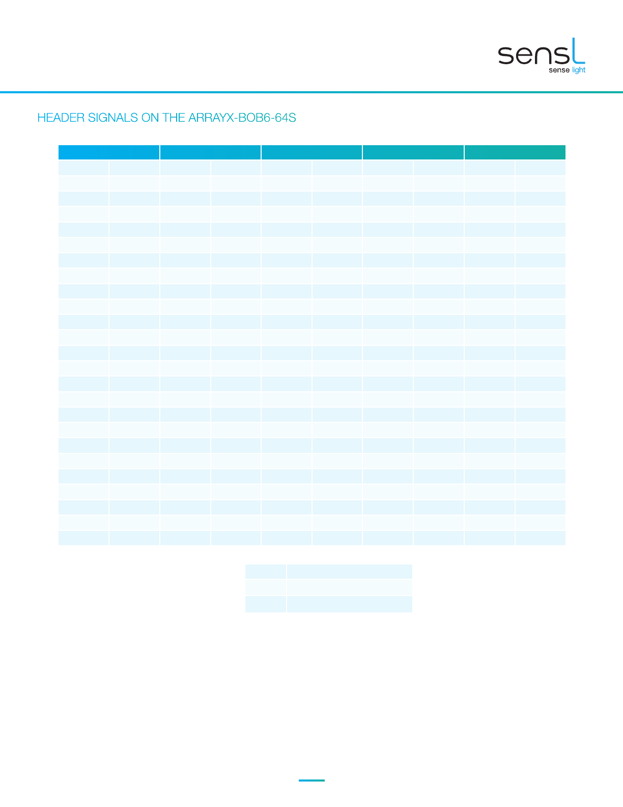
HEADER SIGNALS ON THE ARRAYX-BOB6-64P
NC Not Connected
CM Common I/O
Sn Standard I/O of pixel n
Fn Fast output of pixel n

ArrayJ
USER MANUAL
8
ARRAYX-BOB6-64S (SUMMED BREAKOUT BOARD FOR THE ARRAYJ-60035-64P)
The ArrayX-BOB6-64S is an evaluation board allowing easy access to the sum of all of standard pixel signals of a SensL ArrayJ-
60035-64P, 6 mm 8 x 8 TSV array, in addition to all of the individual fast output signals. The Breakout Board features two
Samtec 80-way connectors, type QSE-040-01-F-D-A. These connectors mate with the Samtec QTE-040-03-F-D-A board-to-
board connector on the array. Since the connectors are keyed, orientating the array on the BOB is straightforward. A schematic
of the board is shown in Figure 4 below.
Fast signals: All of the fast output signals (Fn) from the array are routed via the mating connectors to header pins. These pins are
formed of four 50-way (25 x 2 row) 2.54 mm pitch headers; J3, J4, J5 and J6. Each of the four headers also has 10 pins that
connect to the common cathode (CM) and 8 pins left unconnected (NC) to allow prototyping for evaluation purposes.
Two SMA connectors and Balun transformers are provided with 4-pin headers to allow any fast signal to be connected directly
to the SMA or via the transformer using jumper wires.
Summed output: A summed output (the anodes of pixels 1 to 64 connected together) is routed to jumper pins (SM) in close
proximity to a third SMA connector. Four 7 mm holes are placed on a 25 mm grid to allow mounting of the board on an optical
breadboard.
See Appendix C for an example of the use of the summed BOB.
Figure 4, Layout of the ArrayX-BOB6-64S. The dimensions of the board are 112 mm x 112 mm.
ArrayJ
USER MANUAL
9
Pin J3 J4 J5 J6
12CM CM CM CM CM CM CM CM
3 4 CM CM CM CM CM CM CM CM
5 6 NC NC NC NC NC NC NC NC
78NC NC NC NC NC NC NC NC
9 10 F1 F1 F49 F49 F17 F17 F21 F21
11 12 F9 F9 F57 F57 F25 F25 F29 F29
13 14 F2 F2 F50 F50 F18 F18 F22 F22
15 16 F10 F10 F58 F58 F26 F26 F30 F30
17 18 F3 F3 F51 F51 F19 F19 F23 F23
19 20 F11 F11 F59 F59 F27 F27 F31 F31
21 22 F4 F4 F52 F52 F20 F20 F24 F24
23 24 F12 F12 F60 F60 F28 F28 F32 F32
25 26 CM CM CM CM CM CM CM CM
27 28 F5 F5 F53 F53 F33 F33 F37 F37
29 30 F13 F13 F61 F61 F41 F41 F45 F45
31 32 F6 F6 F54 F54 F34 F34 F38 F38
33 34 F14 F14 F62 F62 F42 F42 F46 F46
35 36 F7 F7 F55 F55 F35 F35 F39 F39
37 38 F15 F15 F63 F63 F43 F43 F47 F47
39 40 F8 F8 F56 F56 F36 F36 F40 F40
41 42 F16 F16 F64 F64 F44 F44 F48 F48
43 44 NC NC NC NC NC NC NC NC
45 46 NC NC NC NC NC NC NC NC
47 48 CM CM CM CM CM CM CM CM
49 50 CM CM CM CM CM CM CM CM
HEADER SIGNALS ON THE ARRAYX-BOB6-64S
NC Not Connected
CM Common cathode I/O
Fn Fast output of pixel n

ArrayJ
USER MANUAL
10
ARRAYJ-60035-4P-BGA (2 X 2ARRAY OF 6 MM PIXELS)
Array Size Sensor
type Readout Board Size Pixel Pitch No. Connections No. Connectors
2 x 2 60035 Pixel 12.46 x 12.46 mm26.33 mm 9 3 x 3 BGA
The ArrayJ-60035-4P is comprised of 4 individual 6 mm J-Series sensors arranged
in a 2 x 2 array.
The performance of the individual pixels and details of the bias to apply can be found
in the J-Series datasheet.
Connections to each sensor are provided by a BGA (ball grid array). The BGA can be
reow soldered onto the user’s own readout board.
The 4 SiPM sensors have all substrate connections (cathodes) connected together
to form a common I/O. The 3 x 3 BGA provides connections as follows:
• 4 x standard I/O
• 5 x common I/O
• There is NO fast output
ARRAYJ-60035-4P-BGA BOARD DIMENSIONS AND PIN LOCATION
The complete ArrayJ-60035-4P-BGA CAD and solder footrprint is available to download.
ArrayJ
USER MANUAL
11
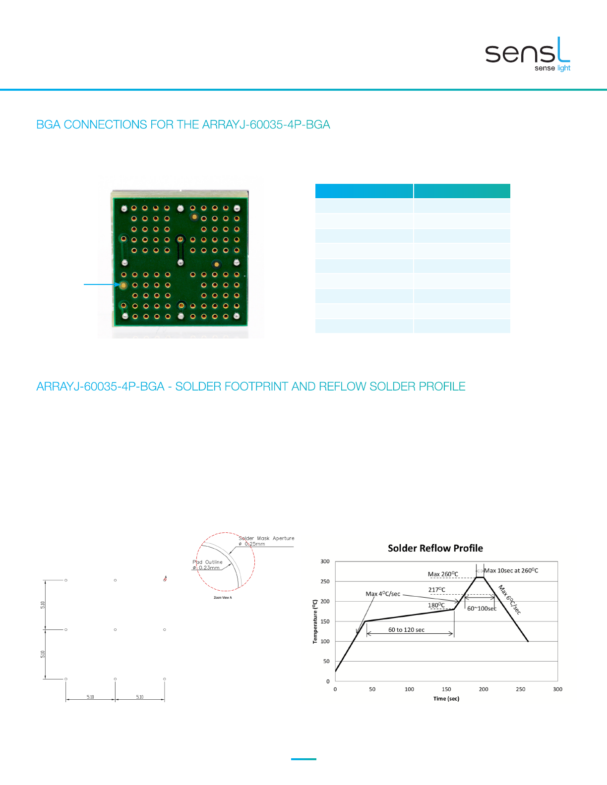
BGA CONNECTIONS FOR THE ARRAYJ-60035-4P-BGA
Pin No. Function
A1 Anode 1
A2 Anode 2
A3 Common Cathode
B1 Anode 3
B2 Anode 4
B3 Common Cathode
C1 Common Cathode
C2 Common Cathode
C3 Common Cathode
The ducial is indicated in the image below. It marks the location of both pin A1 and pixel 1.
ARRAYJ-60035-4P-BGA - SOLDER FOOTPRINT AND REFLOW SOLDER PROFILE
The BGA package is compatible with standard reow solder processes (J-STD-20) and so is ideal for high-volume manufacturing.
The ArrayJ-60035-4P-BGA should be mounted according to specied soldering pad patterns, as shown in Figure 5 and in the
CAD le which can be downloaded here. The solder pads may be oversized to ease placement of the carrier on the PCB.
Consult with your contract manufacturer for recommendation based upon placement accuracy capability.
Solder paste (SensL recommend using no-clean solder paste) must be evenly applied to each soldering pad to insure proper
bonding and positioning of the array. After soldering, allow at least three minutes for the component to cool to room temperature
before further operations.
Solder reow conditions must be in compliance with J-STD-20, table 5.2. This is summarized in Figure 6. The number of
passes should not be more than 2.
Figure 5, Recommended solder footprint for use
with the ArrayJ-60035-4P-BGA
Figure 6, Solder reow prole. Conditions must be in compli-
ance with J-STD-20, table 5.2.
Fiducial

ArrayJ
USER MANUAL
12
ARRAYJ-60035-4P-PCB (ARRAYJ-60035-4P-BGA EVALUATION BOARD)
The ArrayJ-60035-4P-PCB is an evaluation board allowing easy access to
the signals of a ArrayJ-60035-4P-BGA via pins.
The ArrayJ-60035-4P-PCB has the array on the front and pins on the back
of the PCB. The pins are compatible with a standard 8-pin DIL socket for
evaluation purposes. Alternatively, the pins can be directly soldered into
through-holes in the user’s readout PCB. Four of the pins are connected to
the anodes of the individual pixels and the other four pins are connected to
the common cathode. An example mating 8-pin DIL socket is the 110-93-
308-41-001000 from Mill-Max.
The ArrayJ-60035-4P-PCB does NOT provide access to the fast output.
ARRAYJ-60035-4P-PCB PIN-OUTS
Pin No. Function
1Anode 1
2Common Cathode
3Anode 3
4Common Cathode
5Common Cathode
6Anode 4
7Common Cathode
8Anode 2
ARRAYJ-60035-4P-PCB BOARD DIMENSIONS AND PIN LOCATIONS
The complete ArrayJ-60035-4P-PCB CAD is available to download.
PRELIMINARY
ArrayJ
USER MANUAL
13
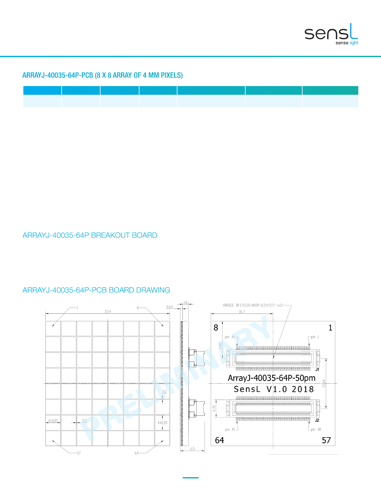
ARRAYJ-40035-64P-PCB (8 X 8ARRAY OF 4 MM PIXELS)
Array Size Sensor type Readout Pixel Pitch Board Size No. Connections No. Connectors
8 x 8 40035 Pixel 4.2 mm 33.4 x 33.4 mm2160 2 x 80-way
The ArrayJ-40035-64P is comprised of 64 individual 4 mm J-Series sensors arranged in a 8 x 8 array. The performance of the
individual pixels and details of the bias to apply can be found in the J-Series datasheet.
Connections to each sensor are provided by two Hirose 80-way connectors, type DF17(2.0)-80DP-0.5v(57). These connectors
mate with the Hirose DF17(2.0)-80DS-0.5v(57) board-to-board connectors. The 64 SiPM sensors have all substrate connections
(cathodes) connected together to form a common I/O. The 2 x 80-way connectors provide connections as follows:
• 64 x fast output
• 64 x standard I/O
• 32 x common I/O
• 4 x shield contacts to the Common
ARRAYJ-40035-64P BREAKOUT BOARD
The breakout board for the ArrayJ-40035-64P-PCB is the same as for the ArrayJ-300XX-64P-PCB: the ArrayJ-BOB3-64P.
Please see page 23 for details.
ARRAYJ-40035-64P-PCB BOARD DRAWING
The complete ArrayJ-40035-64P-PCB CAD is available to download.
PRELIMINARY

ArrayJ
USER MANUAL
14
CONNECTOR SCHEMATICS FOR THE ARRAYJ-40035-64P
Figure 7, Schematic of the ArrayJ-40035-64P connectors.
Figure 8, Highlighting the location of the connector, pin and array pixel numbering on the ArrayJ-40035-64P.
ArrayJ
USER MANUAL
15
CONNECTOR PIN-OUTS FOR THE ARRAYJ-40035-64P
J1 J2
PIN SIGNAL PIN SIGNAL PIN SIGNAL PIN SIGNAL
1S9 2S1 1S41 2S33
3F9 4F1 3F41 4F33
5CM 6S10 5CM 6S42
7S2 8F10 7S34 8F42
9F2 10 CM 9F34 10 CM
11 S11 12 S3 11 S43 12 S35
13 F11 14 F3 13 F43 14 F35
15 CM 16 S12 15 CM 16 S44
17 S4 18 F12 17 S36 18 F44
19 F4 20 CM 19 F36 20 CM
21 S13 22 S5 21 S45 22 S37
23 F13 24 F5 23 F45 24 F37
25 CM 26 S14 25 CM 26 S46
27 S6 28 F14 27 S38 28 F46
29 F6 30 CM 29 F38 30 CM
31 S15 32 S7 31 S47 32 S39
33 F15 34 F7 33 F47 34 F39
35 CM 36 S16 35 CM 36 S48
37 S8 38 F16 37 S40 38 F48
39 F8 40 CM 39 F40 40 CM
41 CM 42 F24 41 CM 42 F56
43 F32 44 S24 43 F64 44 S56
45 S32 46 CM 45 S64 46 CM
47 F23 48 F31 47 F55 48 F63
49 S23 50 S31 49 S55 50 S63
51 CM 52 F22 51 CM 52 F54
53 F30 54 S22 53 F62 54 S54
55 S30 56 CM 55 S62 56 CM
57 F21 58 F29 57 F53 58 F61
59 S21 60 S29 59 S53 60 S61
61 CM 62 F20 61 CM 62 F52
63 F28 64 S20 63 F60 64 S52
65 S28 66 CM 65 S60 66 CM
67 F19 68 F27 67 F51 68 F59
69 S19 70 S27 69 S51 70 S59
71 CM 72 F18 71 CM 72 F50
73 F26 74 S18 73 F58 74 S50
75 S26 76 CM 75 S58 76 CM
77 F17 78 F25 77 F49 78 F57
79 S17 80 S25 79 S49 80 S57
CM Common I/O
Sn Standard I/O
of pixel n
Fn Fast output of
pixel n

ArrayJ
USER MANUAL
16
ARRAYJ-300XX-16P-PCB (4 X 4ARRAY OF 3 MM PIXELS)
Array Size Sensor type Readout Pixel Pitch Board Size No. Connections No. Connectors
4 x 4 30035 Pixel 3.36 mm 13.24 x 13.24 mm240 2 x 20-way
30020
The ArrayJ-300XX-16P is comprised of 16 individual 3 mm J-Series sensors
arranged in a 4 x 4 array. There are two types: The ArrayJ-30035-16P has
pixels which are formed of 35 um microcells, and the ArrayJ-30020-16P has
pixels that are formed of 20 um microcells.
The performance of the individual pixels and details of the bias to apply can
be found in the J-Series datasheet.
Connections to each sensor are provided by two 20-way Hirose plug-type
board-to-board connectors, DF17(2.0)-20DP-0.5V(57). These connectors
mate with the Hirose DF17(3.0)-20DS-0.5V(57). The 16 SiPM pixels have
all substrates (cathodes) connected together to form a common I/O. The 20-
way connector provides connections as follows:
• 16 x fast output
• 16 x standard I/O
• 8 x common I/O
• 4 x shield contacts to the Common
ARRAYJ-300XX-16P-PCB BOARD DRAWING
The complete ArrayJ-300XX-16P-PCB CAD is available to download.

ArrayJ
USER MANUAL
17
CONNECTOR SCHEMATIC FOR THE ARRAYJ-300XX-16P-PCB
Figure 9, Connector pin-outs for the ArrayJ-300XX-16P (left), and the location of the connectors (right).
J1 J2
Pin Signal Pin Signal Pin Signal Pin Signal
1S2 2F1 1S9 2F9
3S1 4F2 3S10 4F10
5S3 6F3 5S11 6F11
7CM 8CM 7CM 8CM
9F4 10 S4 9S12 10 F12
11 F8 12 S8 11 F16 12 S16
13 CM 14 CM 13 CM 14 CM
15 F7 16 S7 15 F15 16 S15
17 F6 18 S6 17 F14 18 S14
19 S5 20 F5 19 S13 20 F13
CM Common I/O
Sn Standard I/O of pixel n
Fn Fast output of pixel n
CONNECTOR PIN-OUTS FOR THE ARRAYJ-300XX-16P-PCB
The array pixel numbering is indicated on the drawing on the previous page.
Connector
Pin 1 locator
Connector labels
Pixel 1 locator
ArrayJ
USER MANUAL
18
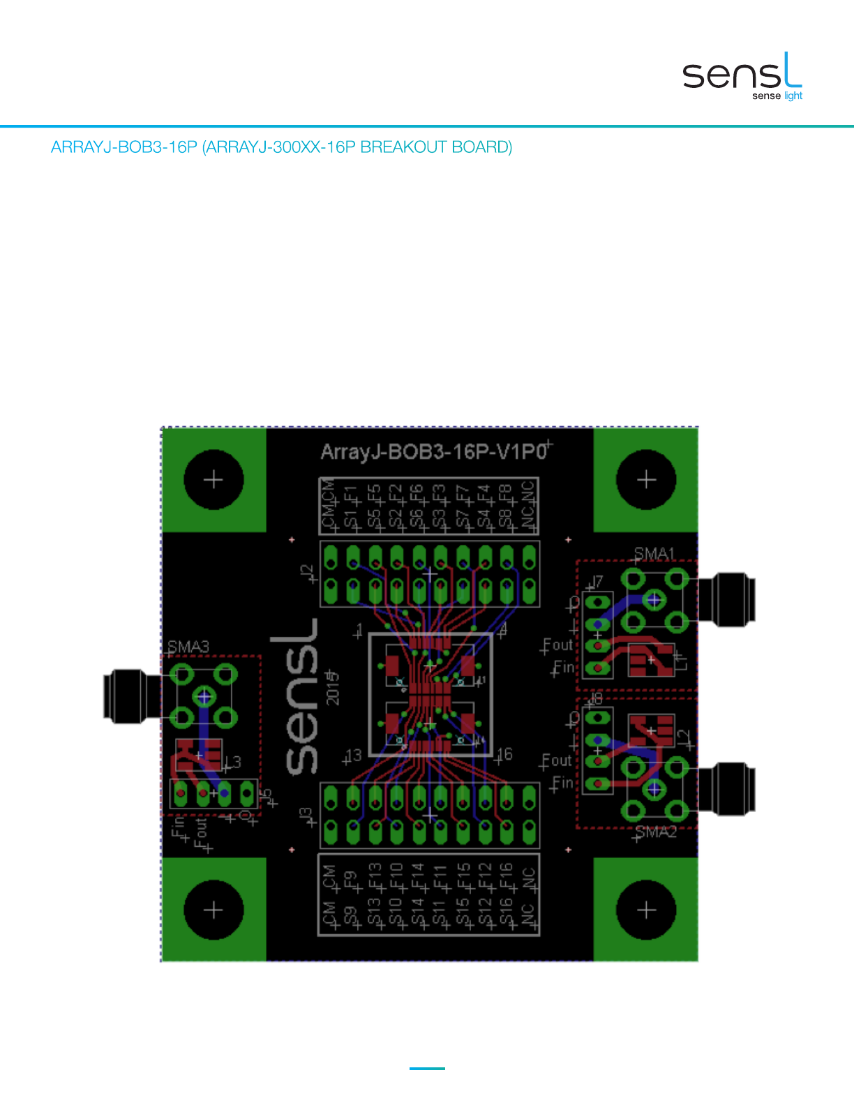
ARRAYJ-BOB3-16P (ARRAYJ-300XX-16P BREAKOUT BOARD)
The ArrayJ-BOB3-16P is an evaluation board allowing easy access to the signals from a SensL ArrayJ-300XX-16P, 3 mm 4 x
4 SiPM array.
The Breakout Board has two HIROSE 20-way connectors DF17(3.0)-20DS-0.5v(57). These connectors mate with the Samtec
DF17(2.0)-20DP-0.5v(57) board-to-board connectors on the array. All signals on the array are routed via the mating connectors
to header pins. These pins are formed by two 20-way (10 x 2 row) 2.54 mm pitch headers.
Three SMA connectors and Balun transformers are provided with 4-pin headers to allow any signal to be connected directly
to the SMA or via the transformer using jumper wires. Four 7 mm holes are aligned on a 25 mm grid to allow mounting of the
board on an optical breadboard.
See Appendices A and B for examples of Breakout Board usage.
Figure 10, Layout of the ArrayJ-BOB3-16P. Note that the array corner pixel numbers are shown on
the silkscreen of the PCB to ensure correct orientation of the array.

ArrayJ
USER MANUAL
19
PIN J2 J3
12CM CM CM CM
3 4 S1 F1 S9 F9
5 6 S5 F5 S13 F13
78S2 F2 S10 F10
9 10 S6 F6 S14 F14
11 12 S3 F3 S11 F11
13 14 S7 F17 S15 F15
15 16 S4 F4 S12 F12
17 18 S8 F6 S16 F16
19 20 NC NC NC NC
HEADER SIGNALS FOR THE ARRAYX-BOB3-16P
NC Not Connected
CM Common I/O
Sn Standard I/O of pixel n
Fn Fast output of pixel n

ArrayJ
USER MANUAL
20
ARRAYJ-300XX-64P-PCB (8 X 8ARRAY OF 3 MM PIXELS)
Array Size Sensor type Readout Pixel Pitch Board Size No. Connections No. Connectors
8x8 30035 Pixel 3.36 mm 26.68 x 26.68 mm2160 2 x 80-way
30020
The ArrayJ-300XX-64P is comprised of 64 individual 3 mm J-Series sensors ar-
ranged in a 8 x 8 array. There are two types: The ArrayJ-30035-64P has pixels
which are formed of 35 um microcells, and the ArrayJ-30020-64P has pixels that
are formed of 20 um microcells.
The performance of the individual pixels and details of the bias to apply can be
found in the J-Series datasheet.
Connections to each sensor are provided by two Hirose 80-way connectors,
type DF17(2.0)-80DP-0.5v(57). These connectors mate with the Hirose DF17(2.0)-
80DS-0.5v(57) board-to-board connectors. The 64 SiPM sensors have all substrate
connections (cathodes) connected together to form a common I/O. The 2 x 80-way
connectors provide connections as follows:
• 64 x fast output
• 64 x standard I/O
• 32 x common I/O
• 4 x shield contacts to the Common
ARRAYJ-300XX-64P-PCB BOARD DRAWING
The complete ArrayJ-300XX-64P-PCB CAD is available to download.
Other manuals for J series
1
This manual suits for next models
14
Table of contents
Other sensl Accessories manuals


