SEPTENTRIO mosaic-X5 User manual
mosaic-X5 Hardware Manual
Version 1.1.0
2
2
2
mosaic-X5 Hardware Manual
Version 1.1.0
October 28, 2019
© Copyright 2000-2019 Septentrio nv/sa. All rights reserved.
Septentrio
Greenhill Campus, Interleuvenlaan 15i
3001 Leuven, Belgium
http://www.septentrio.com
Phone: +32 16 300 800
Fax: +32 16 221 640
@septentrio

3
3
3
1Table of contents
1TABLE OF CONTENTS................................................................................................... 3
2MOSAIC-X5 GNSS MODULE......................................................................................... 6
2.1 Overview................................................................................................................... 6
2.2 Mechanical ............................................................................................................... 7
2.3 Absolute Maximum Ratings................................................................................... 7
2.4 Electrical Characteristics in Operational Conditions.......................................... 8
2.4.1 Power Supply .......................................................................................................... 8
2.4.2 I/O ............................................................................................................................ 8
2.5 Power Consumption................................................................................................ 9
2.6 Environmental ......................................................................................................... 9
3PINOUT AND I/O DESCRIPTION................................................................................ 10
3.1 Power Supply ......................................................................................................... 11
3.2 Antenna .................................................................................................................. 11
3.2.1 Electrical Specifications ........................................................................................ 12
3.3 COM Ports............................................................................................................... 13
3.4 USB Device Interface............................................................................................. 14
3.5 Ethernet.................................................................................................................. 14
3.6 SD Memory Card .................................................................................................... 15
3.7 Clock Frequency Reference.................................................................................. 17
3.7.1 Using the internal TCXO ....................................................................................... 17
3.7.2 Using and external frequency reference ............................................................ 17
3.8 Event/TimeSync inputs ......................................................................................... 18
3.9 PPS output.............................................................................................................. 19
3.10 General Purpose Output (GPx) ............................................................................ 19
3.11 LEDs......................................................................................................................... 20
3.12 Standby................................................................................................................... 20

4
4
4
4MOSAIC-X5 INTEGRATION ........................................................................................ 22
4.1 Minimal Design ...................................................................................................... 22
4.2 Electrical Recommendations ............................................................................... 23
4.3 Decoupling.............................................................................................................. 23
4.4 Layout Recommendations ................................................................................... 23
4.4.1 Coplanarity............................................................................................................ 23
4.4.2 Power..................................................................................................................... 23
4.4.3 Antenna Input ....................................................................................................... 24
4.4.4 Avoiding Self-Interference.................................................................................... 24
5PRODUCT HANDLING................................................................................................ 26
5.1 ESD Precautions..................................................................................................... 26
5.2 Packaging ............................................................................................................... 27
5.3 Part Number .......................................................................................................... 27
5.4 Moisture Sensitivity .............................................................................................. 27
5.5 Soldering................................................................................................................. 27
6DEVELOPMENT KIT .................................................................................................... 29
6.1 Powering the DevKit ............................................................................................. 29
6.2 Antenna Connectors ............................................................................................. 30
6.3 LEDs and General Purpose Output Pins ............................................................. 31
6.4 COM Ports............................................................................................................... 31
6.5 PPS Out and Event Inputs..................................................................................... 32
6.6 Ethernet.................................................................................................................. 33
6.7 USB Dev................................................................................................................... 33
6.8USB Host ................................................................................................................. 33
6.9 REF IN ...................................................................................................................... 33
6.10 Buttons ................................................................................................................... 33
6.11 SD Card Socket ....................................................................................................... 34
APPENDIX A LED STATUS INDICATORS......................................................................... 35

6
6
mosaic-X5 GNSS Module
6
2mosaic-X5 GNSS Module
2.1 Overview
Septentrio mosaic-X5 is a low-power multi-band multi-constellation GNSS receiver
packaged in a 31x31mm LGA module. The internal block diagram is shown below.
The module operates from a single 3V3 power supply (VDD_3V3).
The antenna connects directly to the ANT pin without need for additional components. A
3V to 5.5V DC voltage can be applied to the antenna from the VANT pin. The bias control
circuit detects overcurrent conditions (>150mA) and protects the module in case of short
circuit. See section 3.2.
The module can use its internal TCXO as frequency reference, but also accepts an external
frequency reference on the REF_I pin. See section 3.7.
Two event timer pins and a PPS output are available (1.8V LVTTL). See section 3.8.
The module features a rich set of communication interfaces:
•Four serial ports (3.3V LVTTL), three of them with hardware flow control. See
section 3.3.
•USB. See section 3.4.
•Ethernet (the PHY is external to the module). See section 3.5.

7
7
mosaic-X5 GNSS Module
7
•SDCard interface for logging to an external SD-Card. See section 3.6.
•GPIO and LEDs output. See section 3.10.
2.2 Mechanical
All dimensions in millimeters.
Weight = 6.8g
LGA Details
Specification
Land pitch
1.27 mm
Land diameter
0.6 mm
Pin 1 mark
The A1 pad is missing
Land plating
Nickle/Gold
Array
23 x 23, three outer rows
Number of terminals
239
2.3 Absolute Maximum Ratings
The following conditions should never be exceeded, even momentarily, as it may cause
permanent damage to the module.
Parameter
Comment
Min
Max
Units
VDD_3V3 voltage
See 3.1
-0.3
3.6
V
VDD_BAT voltage
See 3.12
-0.3
3.6
V
VANT voltage
See 3.2
-0.3
5.5
V
8
8
mosaic-X5 GNSS Module
8
3V3_LVTTL input pin voltage
-0.3
VDD_3V3+0.3
V
EVENT input voltage
See 3.8
-0.3
1V8_OUT+0.3
V
RF input power
See 3.2
20
dBm
REF_I level
See 3.7
1.7
Vp-p
Output pins drive current
10
mA
2.4 Electrical Characteristics in Operational Conditions
2.4.1 Power Supply
Parameter
Comment
Min
Typ
Max
Units
VDD_3V3 voltage
See 3.1
3.135
3.3
3.465
V
VDD_BAT voltage
See 3.12
3.135
3.3
3.465
V
VANT voltage
See 3.2
3.0
3.3
5.5
V
USB_VBUS1 voltage
See 3.4
4.4
5.0
5.5
V
1V8_OUT output voltage
1.764
1.8
1.836
V
2V8_OUT output voltage
2.744
2.8
2.856
V
VDD_3V3 current
160
210
500
mA
VDD_BAT input current
0.03
1
mA
USB_VBUS1 input current
See 3.4
10
50
mA
1V8_OUT output current
120
mA
2V8_OUT output current
100
mA
VANT input current
150
mA
2.4.2 I/O
Parameter
Comment
Min
Typ
Max
Units
VIH, 1.8V inputs
0.7*1V8_OUT
V
VIL, 1.8V inputs
0.3*1V8_OUT
V
Input capacitance
1.8V inputs
2.0
pF
Pull-down, 1.8V inputs
80
210
515
kOhm
VOH, 1.8V outputs
7.2 mA
0.75*1V8_OUT
V
VOL, 1.8V outputs
7.2 mA
0.4
V
VIH, 3.3V inputs
0.7*VDD_3V3
VDD_3V3
V
VIL, 3.3V inputs
0
0.3*VDD_3V3
V
Pull-up, 3.3V inputs
Except nRST_IN
68
100
150
kOhm
Pull-up, nRST_IN
9.6
9.8
10
kOhm
VOH, 3.3V outputs
1 mA
VDD_3V3-0.15
V
VIL, 3.3V outputs
1 mA
0.15
V
REF_I input level
0.5
1.7
Vp-p
REF_I input capacitance
8
pF
REF_I input frequency
10
MHz
REF_O output level
See 3.7.1
1.2
Vp-p

9
9
mosaic-X5 GNSS Module
9
2.5 Power Consumption
The module is powered through the VDD_3V3 pins, see section 3.1.
The power consumption depends on the set of GNSS signals enabled and on the
positioning mode. The following table lists the power consumption for some
configurations, while tracking all satellites in view from an open sky, and with the module
at room temperature. The current is applicable to a supply voltage of 3.3V.
GNSS Signals
Positioning
Mode
Power
(mW)
Current
(mA)
GPS L1 C/A
Stand-Alone (1Hz)
550
167
GPS L1/L2
RTK (1Hz)
670
203
GPS/GLONASS L1/L2
RTK (1Hz)
695
211
GPS/GLONASS L1/L2+GALILEO L1/E5a
+BeiDou B1C/B2a (phase 3)
RTK (1Hz)
850
258
GPS/GLONASS L1/L2+GALILEO L1/E5a
+BeiDou B1C/B2a (phase 3)
RTK (100 Hz)
930
282
GPS/GLONASS L1/L2 + L-band
PPP (1Hz)
760
230
All signals from all GNSS constellations
Static (1Hz)
910
276
All signals from all GNSS constellations
+L-band
Static(1Hz)
980
297
All signals from all GNSS constellations
+L-band
Static (100Hz)
1080
327
Enabling wideband interference mitigation with the setWBIMitigation command adds 70
mW.
Minimum power supply drive capability: 0.5A.
2.6 Environmental
Operational: -40 to +85 °C
Storage: -55 to +85 °C
10
10
Pinout and I/O Description
10
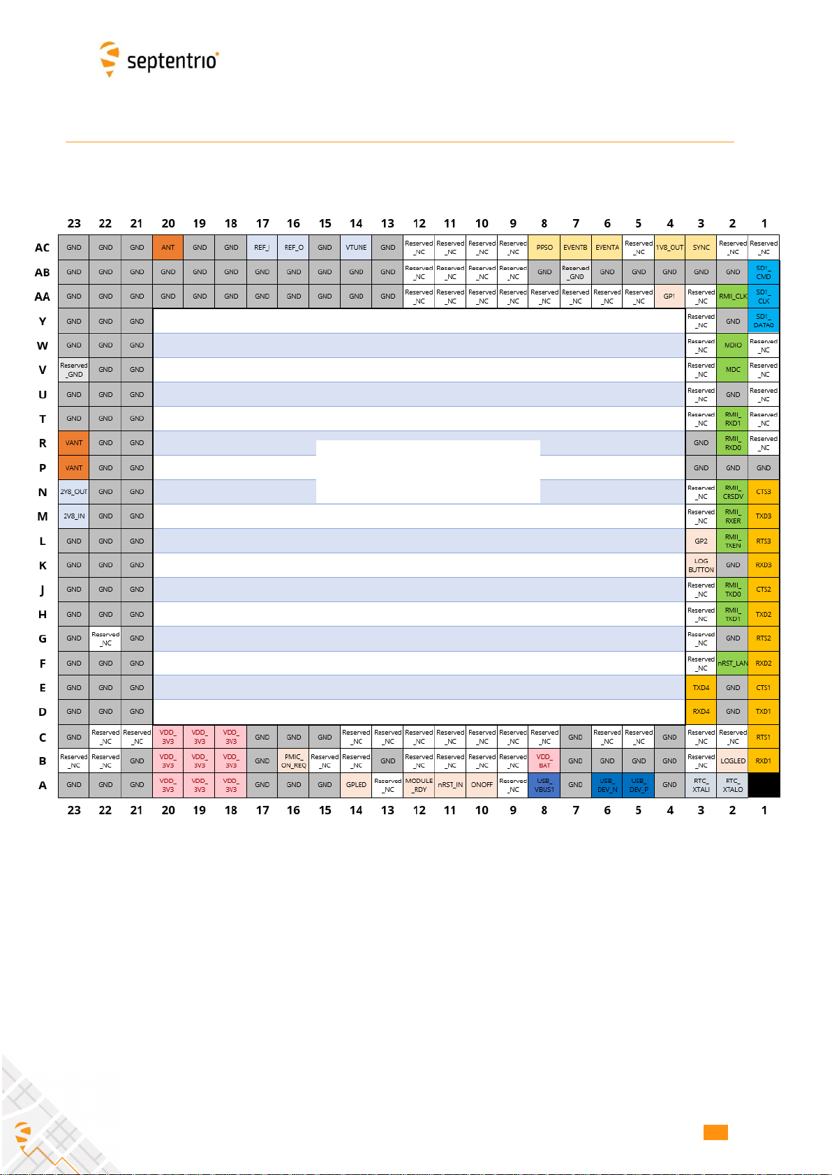
3Pinout and I/O Description
The module provides 239 LGA pads, configured as follows.
The following sections describe all the non-reserved pads. Pads are grouped by functions.
Conventions:
•Pin Type: I=Input, O=Output, P=Power, Ctrl=Control, Clk=Reference clock
•PU: pulled up
•PD: pulled down
•K: keeper input type
TOP VIEW
11
11
Pinout and I/O Description
11
3.1 Power Supply
The module is powered through the VDD_3V3 pins.
Pin Name
Type
Level
Description
Comment
VDD_3V3
P,I
3.3V +/-5%
Main power supply input
All VDD_3V3 pins must be tied
together.
GND
Gnd
0
Ground
All GND pins must be connected to
ground.
VDD_BAT
P,I
3.3V +/-5%
“Always-on” supply.
Must be tied to VDD_3V3 unless an
external power switch is available.
See section 3.12.
nRST_IN
Ctrl,PU
3V3_LVTTL
Reset input, active negative. Module is in reset when low. Short
low pulses of less than 1 µs are ignored.
Internally debounced, can be directly
connected to a push-button.
MODULE_RDY
O
3V3_LVTTL
Level is high when module is operating, and low when in standby
or reset.
Level becomes high about 300
milliseconds after powering /
unresetting the module.
1V8_OUT
P,O
1.8V
1.8V output, see below
SYNC
I
1V8_LVTTL
Reserved. Must always be connected to 1V8_OUT.
Note that the 2V8_OUT and 2V8_IN pins are exclusively reserved to power the internal
TCXO. See section 3.7.
The 1V8_OUT pin is a DC output (120mA max current) which can, for example, be used to
power level-shifters for the 1V8_LVTTL signals (EVENT and PPS), see for example section
3.8.
The module can also control an external power switch, to enable standby mode. See
section 3.12 for details.
3.2 Antenna
The antenna can be directly connected to the ANT pad. The ANT-input is ESD-protected
in the module and carries a DC-voltage to power the antenna, avoiding the need for an
external bias-tee. This DC-voltage is imposed to the module via the VANT-pad.
In case of an overcurrent condition (e.g. short circuit in antenna cable), the module will
first limit the current to about 150 mA and then switch off the antenna supply in about 3
ms. It will periodically retry to switch on the antenna supply until the overcurrent
condition has disappeared.
Refer to 4.4.3 for RF-routing recommendations.
Pin Name
Type
Level
Description
Comment
ANT
RF
RF input
VANT
P,I
3–5.5V
DC supply to the antenna. Max current 150mA. DC supply to
antenna is turned off if overcurrent is detected.
If this pin is not connected or if it is tied to GND, there is no DC
voltage to the antenna.
Never inject an external DC voltage into the ANT-pad as it may damage the module. For
instance, when using a splitter to distribute the antenna signal to several GNSS receivers,
make sure that no more than one output of the splitter passes DC. Use DC-blocks
otherwise.

12
12
Pinout and I/O Description
12
3.2.1 Electrical Specifications
Equivalent DC series impedance at
the ANT pin
2.5 Ohms typical, 3.0 Ohms max
Antenna current limit
150 mA
Antenna net gain range1
15-50 dB
Receiver noise figure2
(NFrx, see Appendix B)
8.5 dB with 15 dB net pre-amplification
18 dB with 25 dB net pre-amplification
26 dB with 35 dB net pre-amplification
35 dB with 45 dB net pre-amplification
RF nominal input impedance
50 Ohms
VSWR
< 2:1 in 1165-1255 MHz and 1525-1610 MHz range
1
The net gain is the total pre-amplification of the distribution network in front of the module. Typically, this
equals antenna active LNA gain minus coax losses in the applicable GNSS bands.
2
The listed noise figure is at room temperature. Add 1 dB for the noise figure at the worst temperature corner
(85°C)
13
13
Pinout and I/O Description
13
3.3 COM Ports
The module provides four serial COM ports. Three of them (COM1 to COM3) support
RTS/CTS hardware flow control:
Pin Name
Type
Level
Description
Comment
TXD1
O
3V3_LVTTL
Serial COM1 transmit line (inactive state is high)
RXD1
I, PU
3V3_LVTTL
Serial COM1 receive line (inactive state is high)
RTS1
O
3V3_LVTTL
Serial COM1 RTS line.
The module drives this pin low when
ready to receive data
CTS1
I, PU
3V3_LVTTL
Serial COM 1 CTS line.
Must be driven low when ready to
receive data from the module.
TXD2
O
3V3_LVTTL
Serial COM2 transmit line (inactive state is high)
RXD2
I, PU
3V3_LVTTL
Serial COM2 receive line (inactive state is high)
RTS2
O
3V3_LVTTL
Serial COM2 RTS line.
The module drives this pin low when
ready to receive data
CTS2
I, PU
3V3_LVTTL
Serial COM3 CTS line.
Must be driven low when ready to
receive data from the module.
TXD3
O
3V3_LVTTL
Serial COM3 transmit line (inactive state is high)
RXD3
I, PU
3V3_LVTTL
Serial COM3 receive line (inactive state is high)
RTS3
O
3V3_LVTTL
Serial COM3 RTS line.
The module drives this pin low when
ready to receive data
CTS3
I, PU
3V3_LVTTL
Serial COM3 CTS line.
Must be driven low when ready to
receive data from the module.
TXD4
O
3V3_LVTTL
Serial COM4 transmit line (inactive state is high)
RXD4
I, PU
3V3_LVTTL
Serial COM4 receive line (inactive state is high)
Unused COM-port signals can be left floating. Flow control is disabled by default.
The COM port settings (baud rate, flow control, etc) are set with the setCOMSettings user
command. The maximum baud rate is 4Mbits/s.
The LVTTL RXD and CTS inputs of the module shall not be driven while its VDD_3V3 input
supply is not present.
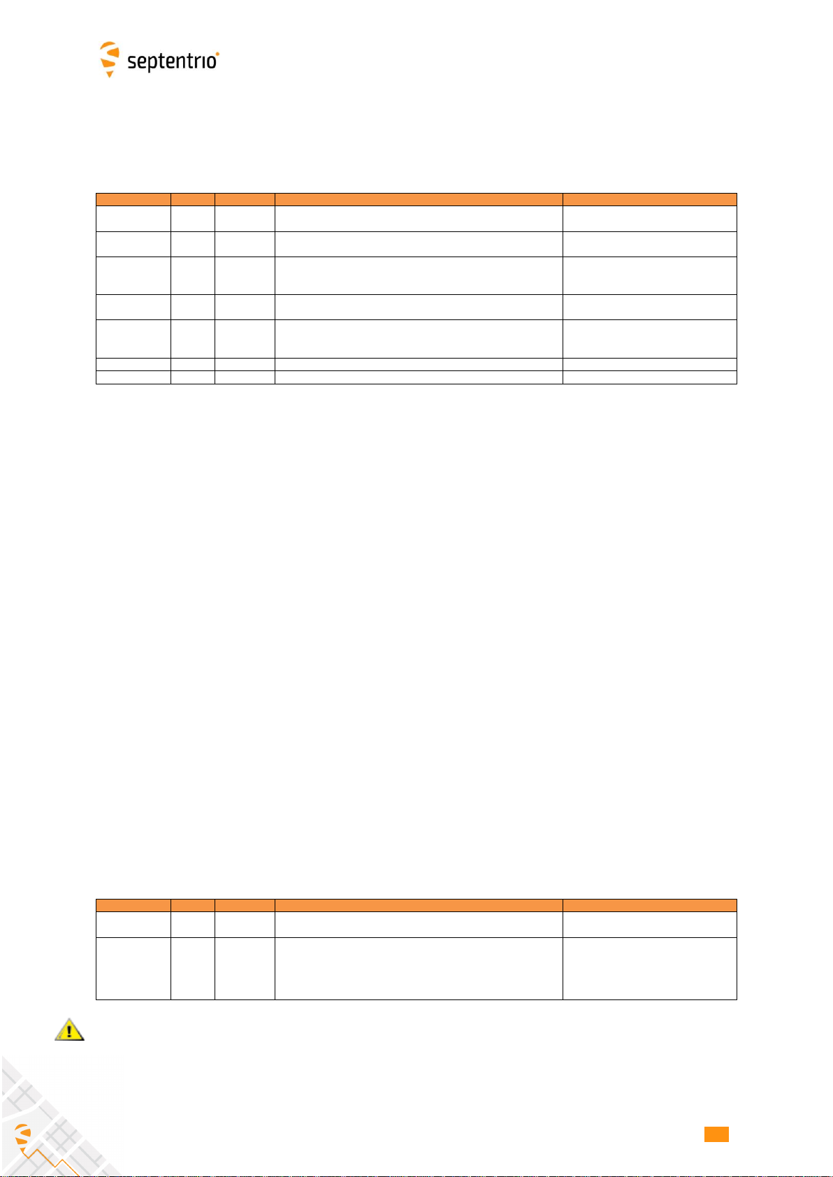
An example of a circuit to convert the COM1 signals to RS232 level is shown below. In
green, the signals to be connected to the mosaic-X5 pins. The RTS1 and CTS1 signals can
be left unconnected if hardware flow control is not required.
14
14
Pinout and I/O Description
14
3.4 USB Device Interface
The following pins are used for accessing the module over USB in USB-device mode.
Pin Name
Type
Level
Description
Comment
USB_VBUS1
P,I
4.40V to
5.5V
USB VBUS input.
This pin cannot be used to power the module.
Maximal current drawn by the module is 50 mA.
USB_DEV_N
I/O
USB
USB data signal, negative
USB_DEV_P
I/O
USB
USB data signal, positive
USB is configured in USB 2.0 mode (high speed, 480Mbps max).
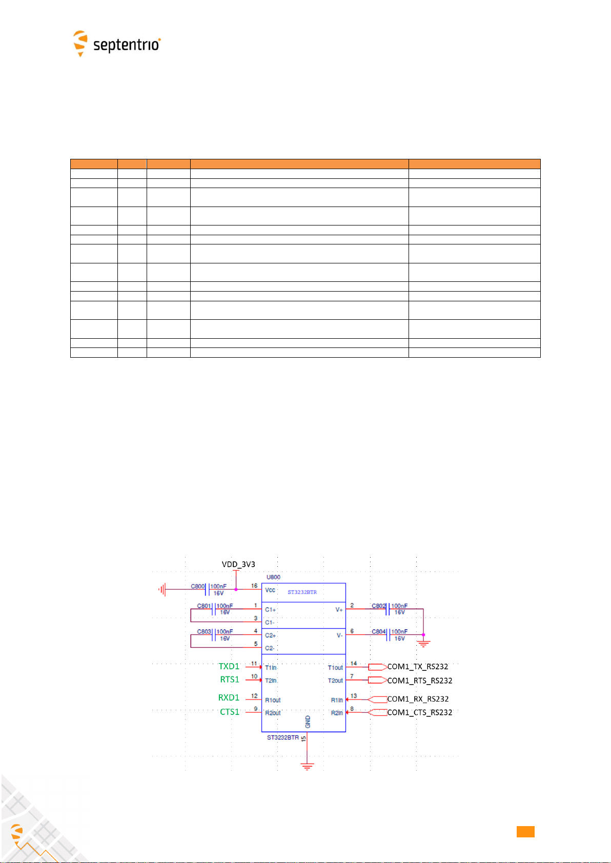
An example of an USB application circuit with ESD protection is shown below. The user
shall make sure to use an ESD-protection and common mode choke compatible with high-
speed USB if this is desired, for instance the USBLC6-2 from ST and DLP31SN121ML2L
from Murata.
3.5 Ethernet
The module supports full duplex 10/100 Base-T Ethernet communication. The Ethernet
PHY and magnetics are to be implemented on the host board. Connection with the PHY
is through the RMII interface available on the following pins:
Pin Name
Type
Level
Description
Comment
RMII_CLK
O
3V3_LVTTL
LAN PHY Clock
MDIO
I/O
3V3_LVTTL
LAN PHY control data
MDC
O
3V3_LVTTL
LAN PHY control clock
RMII_RXD1
I, PU
3V3_LVTTL
LAN PHY receive data 1
RMII_RXD0
I, PU
3V3_LVTTL
LAN PHY receive data 0
RMII_CRSDV
I, PU
3V3_LVTTL
LAN PHY CRS
RMII_RXER
I, PU
3V3_LVTTL
LAN PHY RX error
RMII_TXEN
O
3V3_LVTTL
LAN PHY transmit enable
RMII_TXD0
O
3V3_LVTTL
LAN PHY transmit data 0
RMII_TXD1
O
3V3_LVTTL
LAN PHY transmit data 1
nRST_LAN
O
3V3_LVTTL
LAN reset (low to reset the PHY)
When connecting this pin to enable an
Ethernet PHY, add a 10k pull-down.
If Ethernet is not used, all these pins should be left unconnected.
15
15
Pinout and I/O Description
15
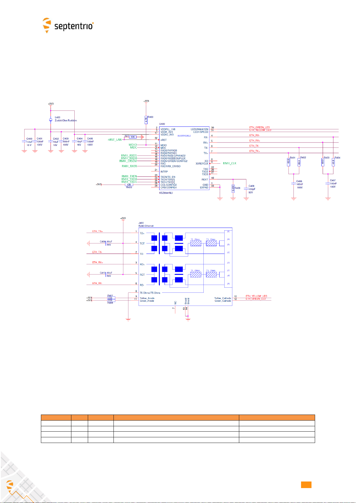
The PHY compatible with the module is the KSZ8041NLI PHY from Microchip.
An application circuit using this PHY and a Würth 74990111217 RJ45 connector with
integrated magnetics is given below. In green, the signals to be connected to the mosaic-
X5 pins.
3.6 SD Memory Card
The module can interface to an external SD memory card through the pins listed in the
table below.
Pin Name
Type
Level
Description
Comment
SD_CLK
O
3V3_LVTTL
SD card CLK line
SD_CMD
O
3V3_LVTTL
SD card CMD line
SD_DAT0
I/O
3V3_LVTTL
SD card DAT0 line
LOGBUTTON
I, PU
3V3_LVTTL
Toggle logging on/off or mount/unmount the disk. See below
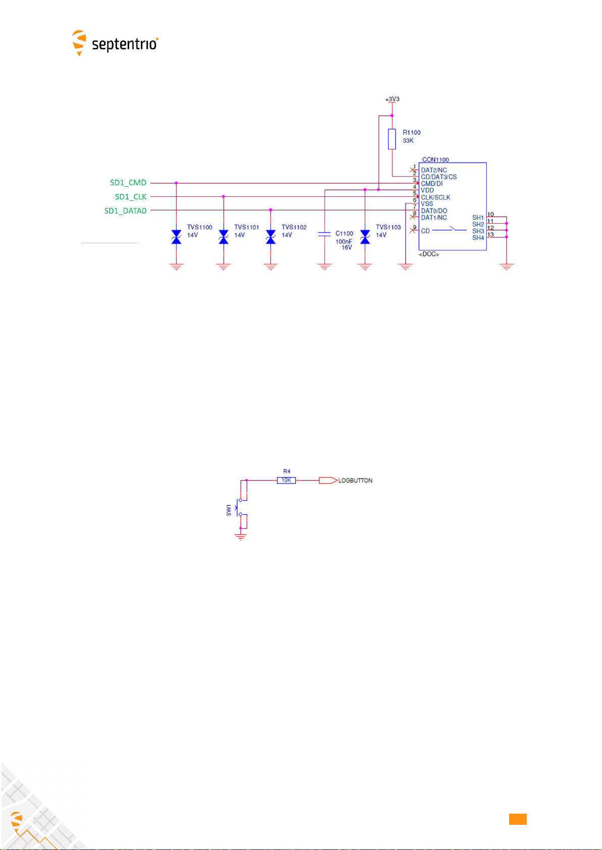
The module supports the 1-bit SD transfer mode with 3V3 signaling. An example circuit
to a 9-pin SD memory card socket is shown below. The maximum clock frequency
(SD_CLK) is 33.000 MHz.
16
16
Pinout and I/O Description
16
Driving the LOGBUTTON pin low for 100 ms to 5 seconds toggles logging on and off.
Driving the LOGBUTTON pin low for more than 5 seconds and then releasing it unmounts
the SD card if it was mounted, or mounts it if it was unmounted. The SD card mount status
can be checked with the LOGLED pin (see Appendix A).
The module debounces the signal in software, so no external debouncing circuit is
required. It is however recommended to add a 1-10 kOhm series resistor with the switch,
to protect the module from voltage spikes.
See instructions in the Reference Guide for details on how to configure SD card logging.
The module is compatible with SD cards of up to 32GB. The file system is FAT32.
When powering off the module while logging, the last seconds of data may be lost. To
avoid data losses, it is advised to first unmount the SD card. This can be done in two ways:
1. By entering the command “exeManageDisk, DSK1, Unmount” before turning off
the module (see the Reference Guide for a description of all the user commands).
2. By driving the LOGBUTTON pin low for at least 5 seconds before turning off the
module.
17
17
Pinout and I/O Description
17
3.7 Clock Frequency Reference
The module can use its internal TCXO frequency reference, or can accept an external
frequency reference, bypassing the internal TCXO.
Pin Name
Type
Level
Description
Comment
REF_I
Clk
0.5-1.7Vp-p
Main frequency reference input, DC-decoupled, input capacitance
is 8 pF
See section 3.7.2.
REF_O
Clk
1.2Vp-p
Frequency reference output from the internal TCXO
See section 3.7.1.
2V8_OUT
P,O
2.8V
2.8V supply output for the internal TCXO.
Do not power any external device from
this pin. It is only intented to connect
to 2V8_IN.
2V8_IN
P,I
2.8V
2.8V supply input for the internal TCXO. Typically connected to
2V8_OUT.
VTUNE
I
Reserved
Leave unconnected.
3.7.1 Using the internal TCXO
To have the module run on its own TCXO:
•REF_I must be connected to REF_O (those pins are next to each other);
•2V8_IN must be connected to 2V8_OUT (those pins are next to each other). Do not
use another 2.8V supply than the one from the 2V8_OUT pin.
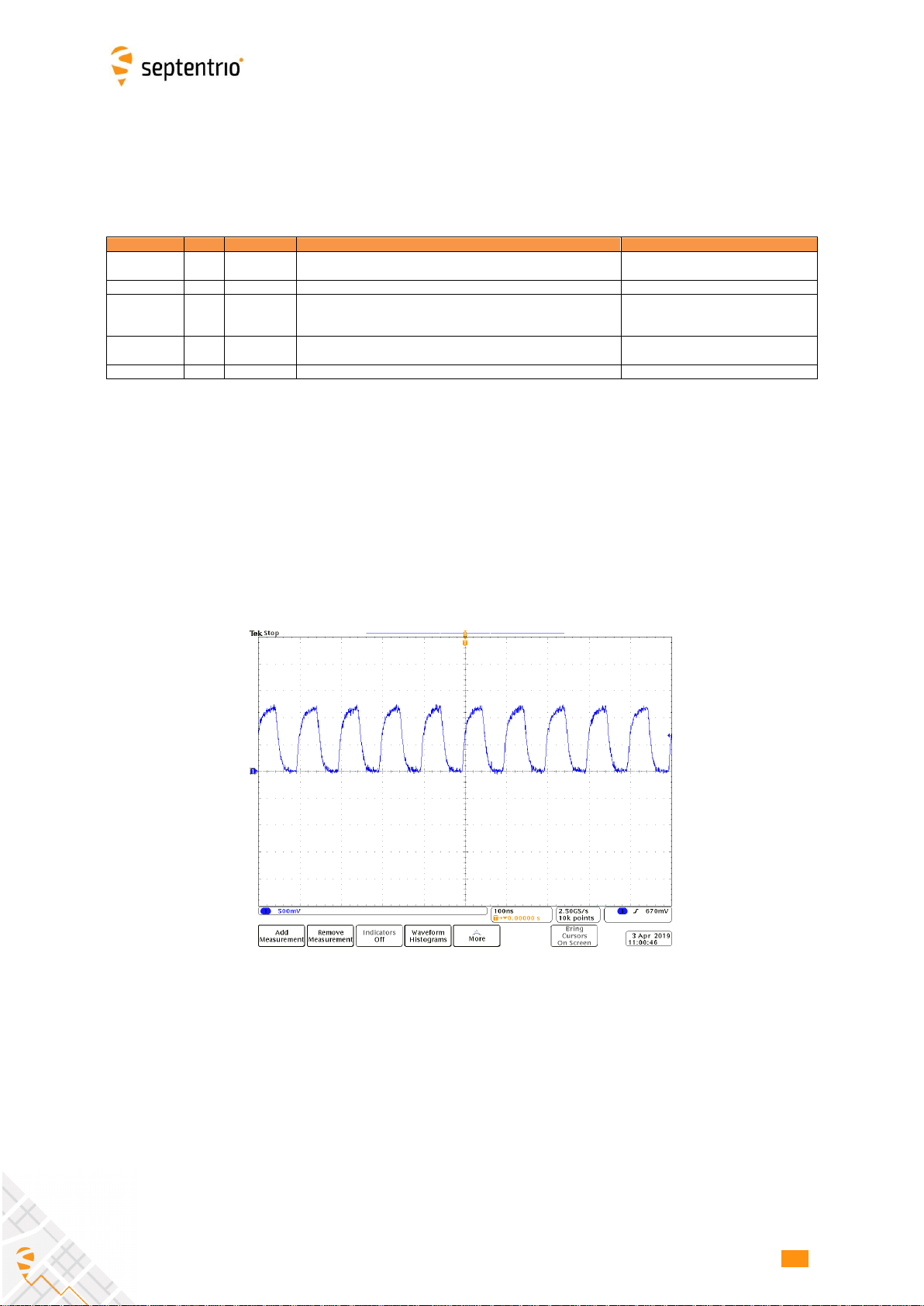
The 10-MHz signal from the internal TCXO is available at the REF_O pin, with peak-to-peak
amplitude of 1.2V. The waveform is illustrated in the oscilloscope screen capture below.
3.7.2 Using and external frequency reference
To use an external frequency reference:
•2V8_IN must be tied to ground
•REF_O and 2V8_OUT are not used and should be left unconnected
•The 10-MHz reference must be fed into the REF_I pin. It is preferably a sine wave
or a band-limited square wave. If CMOS or LVTTL signals are used, it is
recommended to filter them at the source with an RC filter with a pole near 100
MHz. The level at the REF_I input has to be between 0.5 and 1.7 Vp-p. If a higher
signalling voltage is divided with a resistive divider, the impedance level shall be
sufficiently low to avoid excessive level drop because of the filtering of the divider
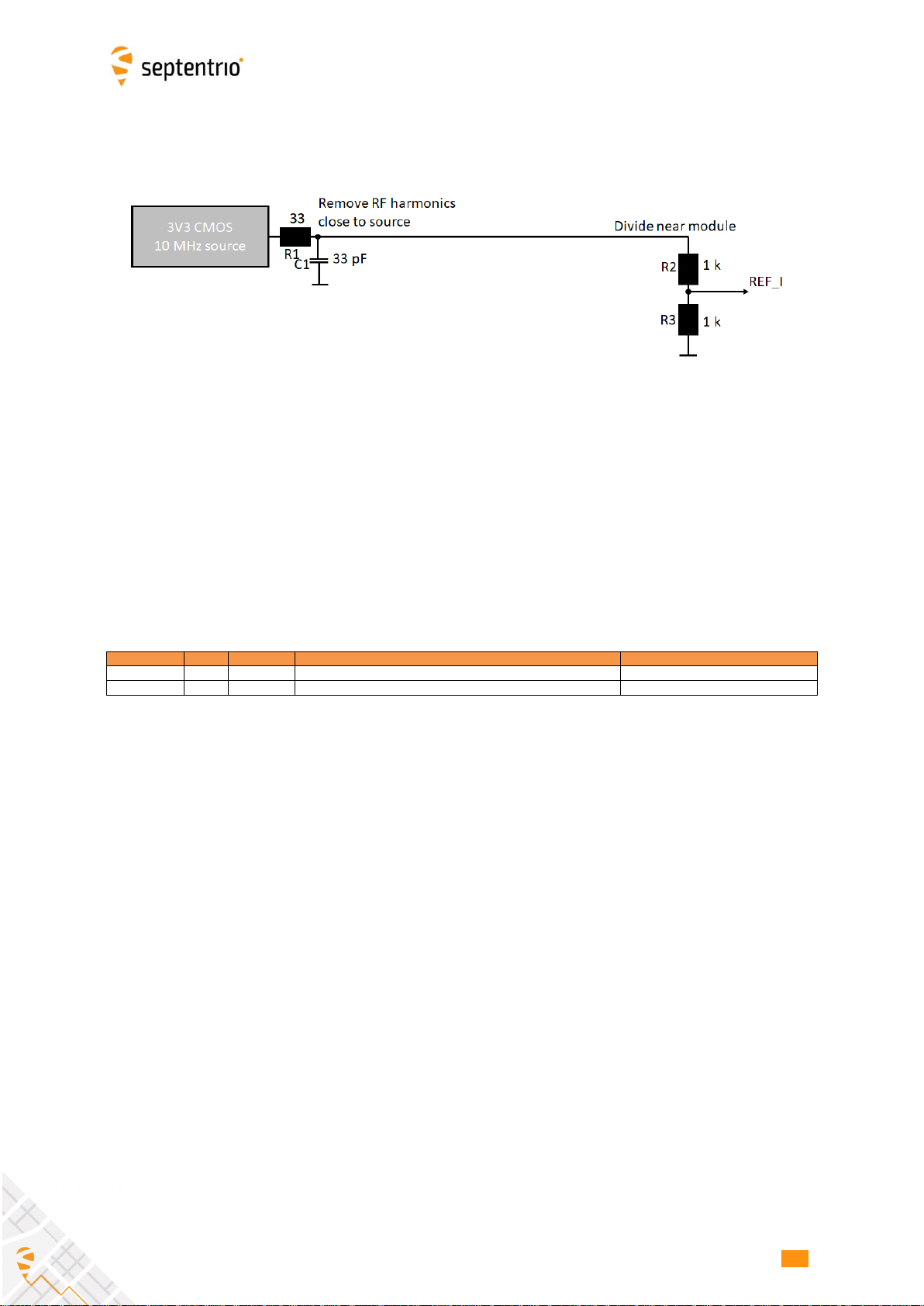
18
18
Pinout and I/O Description
18
with the input capacitance of the REF_I input (8 pF). Below an example circuit. The
module has a build-in DC-decoupling capacitor.
Note that support for an external frequency reference is under permission. Make sure
that the FreqSync permission is enabled to use this feature. Using an external reference
without corresponding permission will cause the module to block most SBF output.
3.8 Event/TimeSync inputs
The module features two event inputs, which can be used to time tag external events with
a time resolution of 20ns.
Pin Name
Type
Level
Description
Comment
EVENTA
I, PD
1V8_LVTTL
Event A or TimeSync input. The pull-down is about 200 kOhm.
Leave unconnected if not used
EVENTB
I, PD
1V8_LVTTL
Event B or TimeSync input. The pull-down is about 200 kOhm.
Leave unconnected if not used
Use the setEventParameters user command to configure the EVENT pins (e.g. to set the
polarity). Note that this feature requires the TimedEvent permission to be enabled in the
module. For correct detection, the minimum time between two events on the same
EVENTx pin must be at least 5ms, and there must be no more than 20 events in any
interval of 100ms, all EVENTx pins considered.
If the TimeSync permission is enabled, the event inputs can also be configured as
TimeSync source using the setTimeSyncSource command. When an event pin is
configured as TimeSync source, the mosaic-X5 expects to see a one-pulse-per-second
(1PPS) signal on that pin. It will then synchronize its internal time base (i.e. the time at
which GNSS measurements are sampled) to that 1PPS signal. TimeSync is typically used
in conjunction with ExtFreq (see section 3.7.2) to fully synchronize the module internal
time base with the time of an external clock.
Note that there is a delay of 15 to 50 ns between the PPS pulse at the EVENT pin and the
module internal time base. That delay is dependent on the phase difference between the
10 MHz frequency at the REF_I pin and the PPS pulse at the EVENT pin. It is possible to
measure this delay by synchronizing the PPS OUT pulse with the internal time base, with
the setPPSParameters,,,,RxClock command.
Note the timing signals use 1.8V logic. If 3.3V logic would be required, the EVENT-signals
can be generated via a resistive divider, considering the integrated pull-down (see 2.4.2).

19
19
Pinout and I/O Description
19
They could as well be created via a level shifter, using the 1V8_OUT output from the
module to supply the module side.
3.9 PPS output
Pin Name
Type
Level
Description
Comment
PPSO
O
1V8_LVTTL
PPS output. Max output current: 10 mA. Polarity and rate user
selectable. During start up, this pin is in high-Z mode.
See Reference Guide for operating instructions.
Default pulse duration: 5ms.
The polarity, frequency and pulse width can be set with the setPPSParameters
command.
The PPSO signal uses 1.8V logic. It can be level-shifted if 3.3V logic is required (e.g. with
SN74AVC4T245RSV).
The PPSO signal is briefly driven high during startup of the module (for about 1 ms), then
gets high-impedant while the module is starting up. It finally gets driven to the intended
level (low or high depending on the user-selected PPS polarity) after a few seconds. If this
start-up behavior is undesirable, it can be shielded by a buffer (or level shifter) with an
output enable. The output enable can be controlled with the MODULE_RDY pin of the
module. The MODULE_RDY signal gets high about 300ms after applying power to
VDD_3V3. The input and output of the buffer should be pulled-up or pulled-down
depending on the desired inactive state of the PPSO signal.
3.10 General Purpose Output (GPx)
The GP1 and GP2 pins are general purpose digital outputs, of which the level can be
programmed with the setGPIOFunctionality command.
Pin Name
Type
Level
Description
Comment
GP1
O
3V3_LVTTL
General purpose output. GP1 in setGPIOFunctionality command.
GP2
O
3V3_LVTTL
General purpose output. GP2 in setGPIOFunctionality command.
20
20
Pinout and I/O Description
20
During the first seconds after powering up the module, these pins are in tristate. Use an
external pull-down or pull-up resistor to have the desired level during boot.
The GPx pins can drive a maximum current of 10mA.
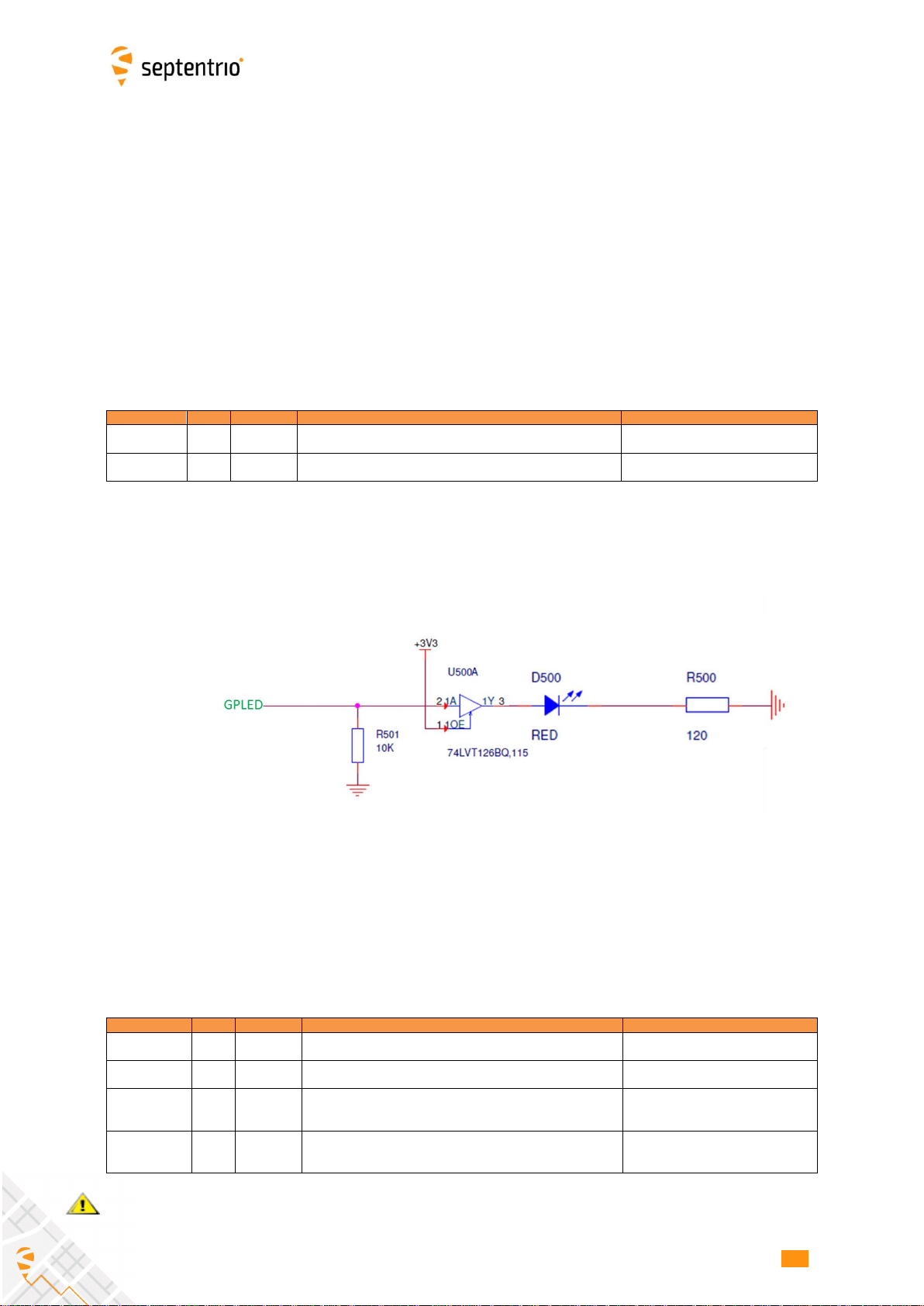
3.11 LEDs
The LED pins can be used to monitor the module status. They can be used to drive
external LEDs. It is assumed that the LED lights up when the electrical level of the
corresponding pin is high. See also Appendix A.
Pin Name
Type
Level
Description
Comment
GPLED
O
3V3_LVTTL
General purpose LED.
Max output current: 10 mA; output impedance: 20 Ohms
LOGLED
O
3V3_LVTTL
Internal logging status indicator.
Max output current: 10 mA; output impedance: 20 Ohms
During boot, i.e. during the first seconds after powering the module, the state of the LEDs
is not defined. Use a pull-down or pull-up resistor to force a desired state.
An example of a circuit with a 10k pull-down and a driver is shown below.
3.12 Standby
The module can control an external power switch, allowing for example to toggle between
standby and active modes upon pressing an “on/off” push-button.
This functionality involves the following pins:
Pin Name
Type
Level
Description
Comment
VDD_3V3
P,I
3.3V +/-5%
Main power supply input, controlled by the external power switch
All VDD_3V3 pins must be tied
together.
VDD_BAT
P,I
3.3V +/-5%
Always-on power supply, which must remain available when
VDD_3V3 is turned off by the external power switch
ONOFF
I, PU
3V3_LVTTL
Typically connected to a push-button to toggle between active
and standby mode. Toggling occurs when the ONOFF pin is driven
low for at least 50ms.
Internally debounced
PMIC_ON_REQ
O
3V3_LVTTL
Typically connected to the control pin of an external power switch.
The power switch is expected to enable VDD_3V3 when
PMIC_ON_REQ is high, and to disable VDD_3V3 when it is low.
The external power switch is optional. When not using an external power switch, always
connect VDD_BAT together with VDD_3V3.
Table of contents
Other SEPTENTRIO Control Unit manuals


