SEPTENTRIO AsteRx-i S User manual

AsteRx-i S and AsteRx-i V
Product Group Hardware Manual
Version 1.0.2

2
2
2
AsteRx-i S and AsteRx-i V Product Group Hardware Manual
Version 1.0.2
September 14, 2018
© Copyright 2000-2018 Septentrio nv/sa. All rights reserved.
Septentrio
Greenhill Campus, Interleuvenlaan 15i
3001 Leuven, Belgium
http://www.septentrio.com
support@septentrio.com
Phone: +32 16 300 800
Fax: +32 16 221 640
@septentrio
3
3
3
1Table of contents
1TABLE OF CONTENTS................................................................................................... 3
2ASTERX-I OEM GNSS MODULE.................................................................................... 8
2.1 Mounting .................................................................................................................. 9
2.2 Environmental ......................................................................................................... 9
2.3 Power and Power Consumption ............................................................................ 9
2.4 RF Interface............................................................................................................ 10
2.4.1 Electrical Specifications............................................................................................ 10
2.4.2 System Noise Figure and C/N0 ............................................................................... 10
2.5 I/O Connectors....................................................................................................... 12
2.5.1 30-pin Connector...................................................................................................... 13
2.5.2 60-pin connector....................................................................................................... 14
2.6 Event Inputs ........................................................................................................... 16
2.7 General Purpose Output (GPx) ............................................................................ 16
2.8 Standby Mode ........................................................................................................ 16
2.9 SD Memory Card Usage ........................................................................................ 16
2.10 USB Interface ......................................................................................................... 17
2.11 Ethernet.................................................................................................................. 18
3SBG ELLIPSE2 MICRO................................................................................................. 20
3.1 Dimensions............................................................................................................. 20
3.2 Environmental ....................................................................................................... 21
3.3 Power Consumption.............................................................................................. 21
3.4 Connector............................................................................................................... 21
3.5 Open-Ended Cable ................................................................................................. 21
4VN-100 RUGGED......................................................................................................... 23
4.1 Dimensions............................................................................................................. 23
4.2 Environmental ....................................................................................................... 24

4
4
4
4.3 Power Consumption.............................................................................................. 24
4.4 Connector............................................................................................................... 24
4.5 Open-Ended Cable ................................................................................................. 25
5ASTERX-I UAS (PRELIMINARY) .................................................................................. 26
5.1 Connectors ............................................................................................................. 27
5.2 Power Supply Options........................................................................................... 28
5.3 LEDs......................................................................................................................... 28
5.4 Temperature Range............................................................................................... 28
5.5 Schematics ............................................................................................................. 28
5.6 UAS to IMU Cables ................................................................................................. 31
DEVELOPMENT KIT ........................................................................................................... 32
5.7 Powering the DevKit ............................................................................................. 32
5.8 Antenna Connectors ............................................................................................. 33
5.9 LEDs......................................................................................................................... 34
5.10 COM Ports............................................................................................................... 34
5.11 PPS Out and Event Inputs..................................................................................... 35
5.12 Ethernet.................................................................................................................. 35
5.13 USB Dev................................................................................................................... 36
5.14 USB Host ................................................................................................................. 36
5.15 REF IN ...................................................................................................................... 36
5.16 Buttons ................................................................................................................... 36
5.17 SD Card Socket ....................................................................................................... 36
5.18 Connection with IMU ............................................................................................ 37
APPENDIX A LED STATUS INDICATORS......................................................................... 38
APPENDIX B EMC CONSIDERATIONS ........................................................................... 40
5
5
5
ROHS/WEEE NOTICE
AsteRx-i complies with European Union (EU) Directive 2002/95/EC on the
restriction of the use of certain hazardous substances in electrical and electronic
equipment (RoHS Directive).
AsteRx-i complies with the European Union (EU) Directive 2002/96/EC on waste
electrical and electronic equipment (WEEE). The purpose of this Directive is the
prevention of waste electrical and electronic equipment (WEEE), and in addition,
the reuse, recycling and other forms of recovery of such wastes so as to reduce
the disposal of waste. If purchased in the European Union, please return the
product at the end of its life to the supplier from which it was purchased.

6
6
6
SAFETY INFORMATION
Statement 0000/WARNING: IMPORTANT SAFETY INSTRUCTIONS
This warning symbol means danger and indicates that you are in a situation that may result in body injury
and physical damage. Before you work on any equipment, be aware of the hazards involved with electrical
circuitry and familiarize yourself with standard practices for preventing accidents. Use the statement number
provided at the beginning of each warning to locate its translation in the translated safety warnings that
accompanied this device.
Statement 0001/WARNING: The power supply provided by Septentrio (if any) should not be replaced by
another. If you are using the receiver with your own power supply, it must have a double isolated construction
and must match the specifications of the provided power supply.
Statement 0003/WARNING: Ultimate disposal of this product should be handled according to all national
laws and regulations.
Statement 0005/WARNING: The equipment and all the accessories included with the product may only
be used according to the specifications in the delivered release note, in the manual and in all other documents
delivered with the receiver.
Statement 0007/WARNING: Never place the equipment in direct sunlight.

7
7
7
WARNING: Handling of ESD Sensitive Devices
Electrostatic discharge is a sudden flow of current from one object to another either object or to
ground. Electrostatic charges can accumulate on common items such as polystyrene drinking cups,
cellophane tape, synthetic clothing, untreated foam packaging material, and untreated plastic bags
and work folders, to name but a few.
Electronic components and assemblies can be permanently damaged or destroyed when near or
in contact with electro-statically charged objects. When you handle components or assemblies that
are not in protective bags and you are not sure whether they are static-sensitive, assume that they
are static-sensitive and handle them accordingly.
Everyone who is working with ESD-sensitive devices must be aware of these rules.
General rules
Always test your ground strap, bench mat, conductive work surface, and ground cord before either
removing components and assemblies from their protective bags or before beginning any
disassembly or assembly procedures. Perform all service procedures in a static-protected
environment. Always use techniques and equipment designed to protect personnel and
equipment from electrostatic discharge.
Handling
•Remove static-sensitive components and assemblies from their static-shielding bags only at
static-safe workstations - a properly grounded table and grounded floor mat - and only when
you are wearing a grounded wrist strap (with a resistor of at least 1 mega-ohm in series) or
other grounding device. Avoid having non-ESD safe material on the workbench. Clear the
work station of static generators like e.g. polyethylene, vinyl’s, foam, notebooks, document
holders, etc.
•Use only grounded tools when manipulating static-sensitive components and assemblies.
•Place and seal static-sensitive components and assemblies in their original static-shielding
bags before removal from static-protected areas.
•Stacking of board assemblies should be avoided to prevent physical damage to devices.
Transport & Storage
•Limit as much as possible the manipulation of ESD-sensitive devices and components.
•Handle ESD-sensitive parts as far as possible in their (original) protective packaging.
•Protect ESD-sensitive components against dust as this is a possible carrier of static loads.
Assembled printed circuit boards (PCB’s) must always be placed in an anti-static shielding
bag, box or PCB containers during transport between workplaces or to a warehouse.

8
8
AsteRx-i OEM GNSS Module
8
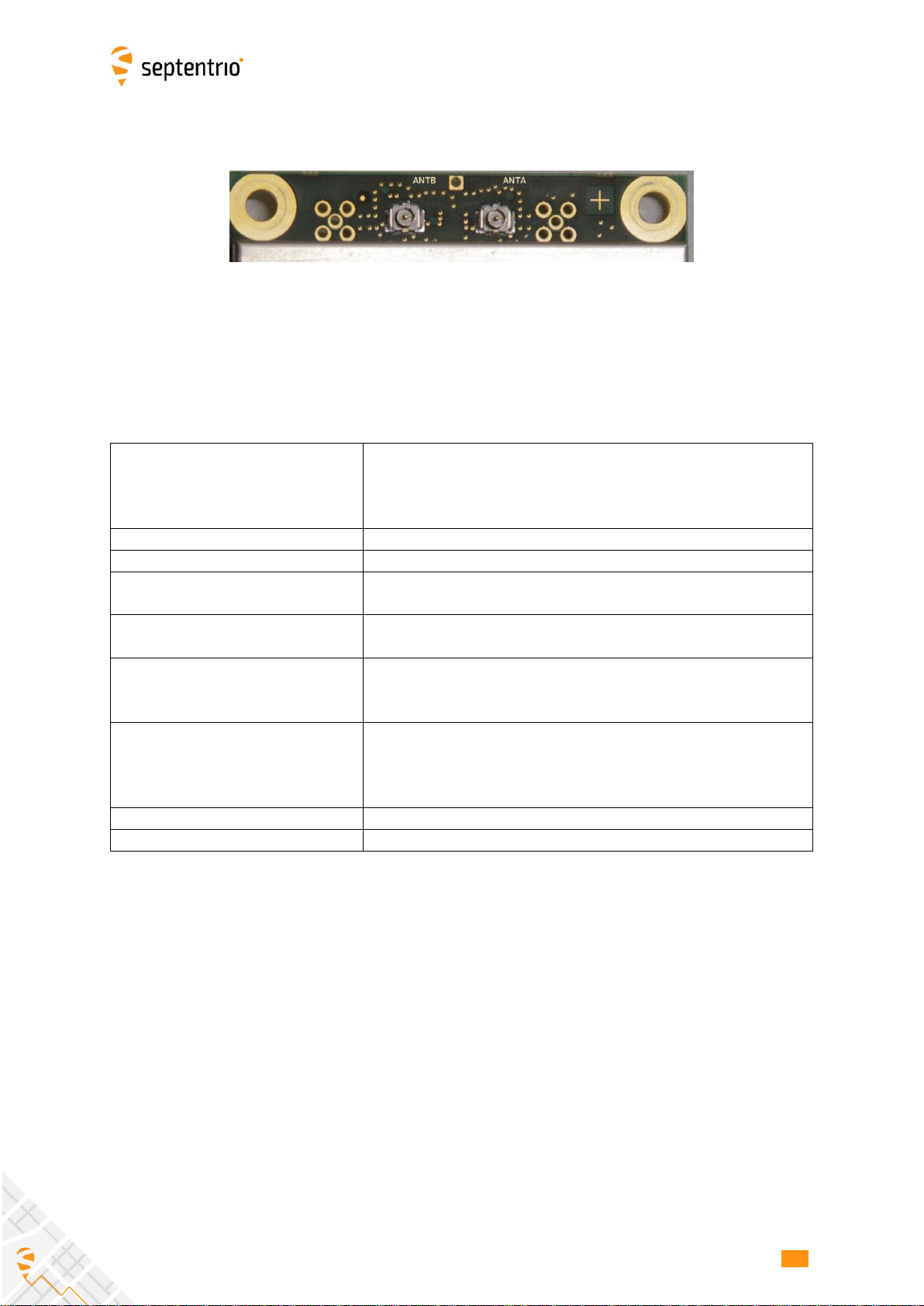
2AsteRx-i OEM GNSS Module
All dimensions in millimeters.
Weight = 28 g
RF connectors (u.FL type) are mounted on top side of the PCB. The 30- and 60-pin Hirose
I/O connectors are mounted on the bottom side.
view from above,
I/O connectors on
the bottom side
Pin#1
Pin#1
9
9
AsteRx-i OEM GNSS Module
9
2.1 Mounting
The four mounting holes are compatible with M3 screws. Use M3 3.5mm spacers. An
example of applicable SMD spacer is THF-1.6-3.5-M3 from MAC8.
All mounting holes are grounded, and should preferably be connected to ground on the
host PCB. Note however that the mounting holes should not be relied on as only ground
return connection: a proper ground should be supplied to the GND pins of the I/O
connector(s) as well.
2.2 Environmental
Operational: -40 to +85 °C
Storage: -55 to +85 °C
2.3 Power and Power Consumption
The OEM module is powered through pin#1 and pin#2 of the 30-pin connector. Power
supply voltage must be 3.3V +/-5%.
The power consumption depends on the set of GNSS signals enabled with the
setSignalTracking command.
The following table shows the typical power consumption of the OEM module (not
including the IMU) in dual-antenna mode for selected sets of signals:
Signals enabled with setSignalTracking
Power
consumption
GPS L1+L2
1000 mW
GPS L1+L2, GLO L1+L2
1050 mW
All GNSS signals from all GNSS constellations
1115 mW
Enabling wideband interference mitigation with the setWBIMitigation command adds 80
mW.
Consumption in standby mode: 10 mW
In-rush current: 1.3 A during less than 100 µs
Maximum peak current during operation: 0.5 A
10
10
AsteRx-i OEM GNSS Module
10
2.4 RF Interface
The main antenna must be connected to the ANTA u.FL and the auxiliary antenna must
be connected to the ANTB u.FL connector.
2.4.1 Electrical Specifications
Antenna supply voltage
3-5.5V DC, set via pin#18 of the 30-pin connector. The DC
voltage is applied to both antenna connectors.
If pin#18 is not connected, there is no DC voltage to the
antennas.
ANTA DC series impedance
< 2.2 Ohms
ANTB DC series impedance
< 4 Ohms
Guaranteed antenna current
(ANTA or ANTB)
200 mA
Antenna current limit (ANTA or
ANTB)
< 300 mA
Antenna net gain range1
15-45 dB
For optimal performances, the net gain on ANTA and ANTB
must not differ by more than 10dB.
Receiver noise figure
(NFrx, see below)
10 dB (with 15-dB net gain)
The receiver noise figure increases as the net gain increases,
but its contribution to the system noise figure decreases.
The worse case is for a net gain of 15dB.
RF nominal input impedance
50 Ohms
VSWR (ANTA or ANTB)
< 2.5:1 in 1200-1251 MHz and 1560-1610 MHz range
1 The net gain is the total pre-amplification of the distribution network in front of the receiver. Typically, this
equals antenna active LNA gain minus coax losses in the applicable GNSS bands.
2.4.2 System Noise Figure and C/N0
The system noise figure, in dB, can be calculated as:
NFsys = 10*log10(10NFant/10 + (10NFrx/10-1)/10Gpreamp/10)
where
•NFant is the antenna LNA noise figure, in dB.
•NFrx is the receiver noise figure, in dB. NFrx depends on the net gain, but a good
approximation (<0.5dB) of NFsys can be obtained by setting NFrx = 10dB.
•Gpreamp is the net gain in front of the receiver, in dB.
11
11
AsteRx-i OEM GNSS Module
11
For example, with a 2.5-dB antenna LNA noise figure, 30-dB antenna LNA gain and 15-dB
cable loss, Gpreamp = 30dB-15dB = 15dB. In this case, the system noise figure is:
NFsys = 10.log10(102.5/10+ (1010/10-1)/1015/10) = 3.14 dB.
The C/N0, in dB-Hz, of a GNSS signal received at a power P can be computed by:
C/N0 = P - 10.log10(Tant + 290*(10NFsys/10-1)) + 228.6 dB
where
•P is the received GNSS signal power including the gain of the antenna passive
radiating element, in dBW (e.g. -155dBW)
•Tant is the antenna noise temperature, in Kelvin. Typically Tant = 130K for an open-
sky antenna.
•228.6 is -10*log10(kB) with kB=1.38e-23 J/K the Boltzmann constant.

12
12
AsteRx-i OEM GNSS Module
12
2.5 I/O Connectors
The main connector is the 30-pin connector. That connector must always be connected.
The 60-pin connector provides additional signals (IO enable, serial CTS/RTS lines, GPIOs,
Ethernet, 10-MHz reference input, etc). That connector can be ignored and left
unconnected if these signals are not needed.
Warnings
•All ground pins must be connected (not applicable to the 60-pin connector if that
connector is not used).
•Do not drive a non-zero voltage into input pins (pins type “I”in the tables below)
when the receiver is not powered or is in standby (see section 2.8), and during the
first 300 ms after these states. The IO_EN pin of the 60-pin connector indicates
when the board is ready to accept input, and can be used to enable the drivers
driving the input pins. Designs not using the 60-pin connector must either keep
the input pins in hi-Z mode for at least 300 ms after applying power, or drive the
nRST pin low for at least 300 ms after applying power. When not using the IO_EN
pin, it is recommended not to put the board in standby mode.
•When pull-up/down resistors are needed, use 10 k.
•Unused or reserved pins should be left unconnected unless explicitly mentioned
otherwise.
•In applications where the antenna is located close to the GNSS module, it is good
practice to route all high-speed digital signals (e.g. the SD card signals) in inner
layers of the host PCB, with ground copper at top and bottom layers. This is to
prevent interference into the GNSS signals.
Conventions
•Pin Type: I=Input, O=Output, P=Power, Ctrl=Control, Clk=Reference clock
•LVTTL=3V3 Low Voltage TTL: VIL≤ 0.8V, VIH≥ 2.0V, VOL≤ 0.4V, VOH≥ 2.4V.
•PU: internally pulled up
•PD: internally pulled down
•K: keeper input type
60 pin
30 pin
13
13
AsteRx-i OEM GNSS Module
13
2.5.1 30-pin Connector
Connector type: Hirose 30 pins DF40HC (3.5)-30DS-0.4V(51)
Mating connector: Hirose DF40C-30DP-0.4V(51)
See the pin numbering convention in the above picture.
Pin#
Name
Type
Level
Description
Comment
1
Vin
P
3.3V
+/-5%
Main power supply input
Both Vin pins (pin#1 and pin#2) must
be tied together.
3
GND
Gnd
0
Ground.
5
USB_D+
I/O
USB
USB data signal positive D+.
7
USB_Vbus
Ctrl
4.40V
≤V≤
5.25V
USB VBUS.
This pin cannot be used to power the receiver!
Mandatory if USB is used.
See section 2.10
9
TX1
O
LVTTL
Serial COM 1 transmit line (inactive state is high)
11
GND
Gnd
0
Ground.
13
TX2
O
LVTTL
Serial COM 2 transmit line (inactive state is high)
15
TX3
O
LVTTL
Serial COM 3 transmit line (inactive state is high)
17
GND
Gnd
0
Ground.
19
EventA
I, PD
LVTTL
Event A input.
See section 2.6
21
Reserved
Reserved
23
GND
Gnd
0
Ground.
25
Button
I, K
LVTTL
Input can be connected to a push button used to control SD card
logging. Low state is interpreted as “button pressed”.
Debouncing must be done externally
(no debouncing circuit on board).
See also section 2.9.
27
LOGLED
O
LVTTL
Internal logging status indicator.
Max output current: 10 mA; output impedance: 20 Ohms
See Appendix A
29
GND
Gnd
0
Ground.
Pin#
Name
Type
Level
Description
Comment
2
Vin
P
3.3V
+/-5%
Main power supply input
Both Vin pins (pin#1 and pin#2) must be
tied together.
4
GND
Gnd
0
Ground.
6
USB_D-
I/O
USB
USB data signal negative D-.
8
nRST
Ctrl,PU
LVTTL
Reset input, active negative. Receiver resets when driven low.
10
RX1
I, K
LVTTL
Serial COM 1 receive line (inactive state is high).
12
PPSout
O
LVTTL
PPS output. Output impedance: 50 ohms. Output current: 24 mA.
Polarity and rate user selectable. During start up, this pin is pulled
low with a 100-kOhm resistor.
See Reference Guide for operating instructions. Pulse duration: 5ms.
14
RX2
I, K
LVTTL
Serial COM 2 receive line (inactive state is high).
16
RX3
I, K
LVTTL
Serial COM 3 receive line (inactive state is high).
18
VANT
P
3<
VANT
< 5.5V
Antenna supply.
See section 2.4.1
20
nPDN
Ctrl,PU
LVTTL
Receiver is put in standby mode (low power mode) when driven low.
Normal operation resumes when the pin level is high.
22
GPLED
O
LVTTL
General purpose LED.
Max output current: 10 mA; output impedance: 20 Ohms
See Appendix A
24
Reserved
26
SD_CLK
O
LVTTL
SD card CLK line
See section 2.9
28
SD_CMD
O
LVTTL
SD card CMD line
See section 2.9
30
SD_DAT0
I/O
LVTTL
SD card DAT0 line
See section 2.9
1
29
30
2

14
14
AsteRx-i OEM GNSS Module
14
2.5.2 60-pin connector
Connector type: Hirose DF40C-60DP-04V(51)
Mating connector: Hirose DF40HC(3.5)-60DS-0.4V(51)
See the pin numbering convention in the above picture.
Pin#
Name
Type
Level
Description
Comment
1
Reserved
3
Reserved
5
Reserved
7
Reserved
9
GP1
O
LVTTL
General purpose output. GP1 in setGPIOFunctionality command.
See section 2.7
11
RTS2
O
LVTTL
Serial COM2 RTS line. The AsteRx-i OEM drives this pin low when
ready to receive data.
13
RTS3
O
LVTTL
Serial COM3 RTS line. The AsteRx-i OEM drives this pin low when
ready to receive data.
15
TX4
O
LVTTL
Serial COM 4 transmit line (inactive state is high)
17
Reserved
19
Reserved
21
Reserved
23
Reserved
25
Reserved
27
Reserved
29
GND
Gnd
Ground
31
RMII_TXEN
O
LVTTL
LAN PHY transmit enable
See section 2.11
33
RMII_TXD1
O
LVTTL
LAN PHY transmit data 1
See section 2.11
35
RMII_CRS_DV
I
LVTTL
LAN PHY CRS
See section 2.11
37
RMII_RXER
I
LVTTL
LAN PHY RX error
See section 2.11
39
Reserved
41
Reserved
43
Reserved
45
Reserved
47
Reserved
49
Reserved
51
Reserved
53
Reserved
55
Reserved
57
EventB
I,PD
LVTTL
Event B input.
See section 2.6
59
IO_EN
O
LVTTL
Level is high when board is in normal operating conditions and it is
safe to drive the input pins (see warnings on page 12)
2
59
1
60

15
15
AsteRx-i OEM GNSS Module
15
Pin#
Name
Type
Level
Description
Comment
2
Reserved
4
GND
Gnd
Ground
6
Reserved
8
GND
Gnd
Ground
10
Reserved
12
CTS2
I, K
LVTTL
Serial COM 2 CTS line. Must be driven low when ready to receive
data from the AsteRx-i OEM.
14
CTS3
I, K
LVTTL
Serial COM 3 CTS line. Must be driven low when ready to receive data
from the AsteRx-i OEM.
16
RX4
I, K
LVTTL
Serial COM 4 receive line (inactive state is high).
18
GND
Gnd
Ground
20
Reserved
22
Reserved
24
Reserved
26
Reserved
28
Reserved
30
GND
Gnd
Ground
32
RMII_CLK
O
LVTTL
LAN PHY Clock
See section 2.11
34
RMII_TXD0
O
LVTTL
LAN PHY transmit data 0
See section 2.11
36
GND
Gnd
Ground
38
RMII_RXD0
I
LVTTL
LAN PHY receive data 0
See section 2.11
40
RMII_RXD1
I
LVTTL
LAN PHY receive data 1
See section 2.11
42
GND
Gnd
Ground
44
GP2
O
LVTTL
General purpose output. GP2 in setGPIOFunctionality command.
See section 2.7
46
Reserved
48
Reserved
50
GND
Gnd
Ground
52
Reserved
54
MDIO
I/O
LVTTL
LAN PHY control data
See section 2.11
56
MDC
O
LVTTL
LAN PHY control clock
See section 2.11
58
GND
Gnd
Ground
60
Reserved

16
16
AsteRx-i OEM GNSS Module
16
2.6 Event Inputs
The receiver features two event inputs (EventA on the 30-pin connector, and EventB on
the 60-pin connector), which can be used to time tag external events. Use the
setEventParameters command to configure these pins (e.g. to set the polarity). Note
that this feature requires the TimedEvent (event marker) permission to be enabled in the
receiver.
2.7 General Purpose Output (GPx)
The GP1 and GP2 pins of the 60-pin connector are general purpose LVTTL digital outputs,
of which the level can be programmed with the setGPIOFunctionality command.
During the first seconds after powering up the board, these pins are in tristate. Use an
external pull-down or pull-up resistor to have the desired level during boot.
The GPx pins can drive a maximum current of 10mA.
2.8 Standby Mode
In standby mode, all receiver functions are turned off and the power consumption is very
low (see section 2.3). There are two ways to enter standby mode:
1. By driving the nPDN pin low (pin#20 of the 30-pin connector). The receiver wakes
up when the nPDN pin level is high again (there is an internal pull-up).
2. By entering the “exePowerMode, StandBy” user command. To wake up, the nPDN
pin should be shortly driven low (at least for 50ms).
It is also possible to schedule automatic standby/wakeup periods using the
setWakeUpInterval command.
Note that entering standby mode takes a few seconds during which all running processes
are shutdown.
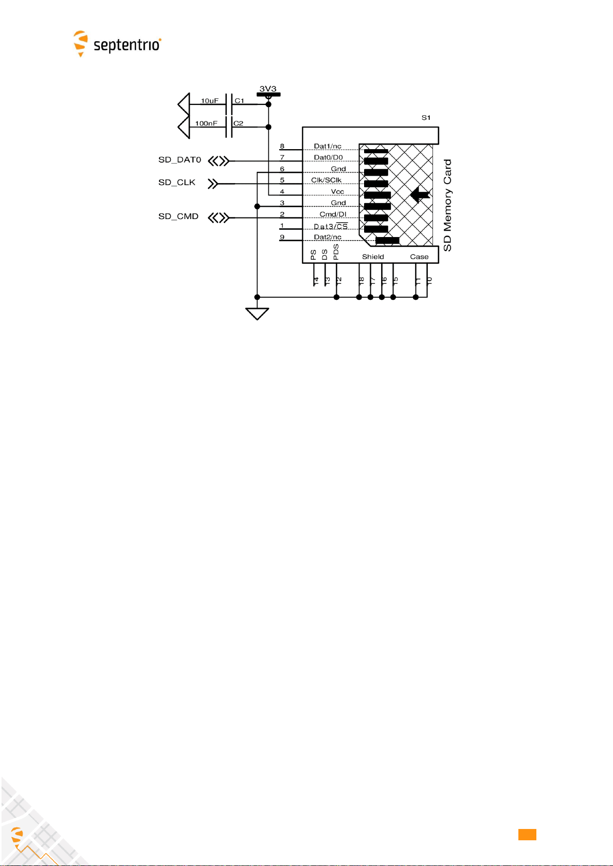
2.9 SD Memory Card Usage
The receiver can interface to an external SD memory card through the SD-card pins of the
30-pin connector. The receiver supports the 1-bit SD transfer mode with 3V3 signaling.
An example circuit to a 9-pin SD memory card socket is shown below. The maximum clock
frequency (SD_CLK) is 33.000 MHz.
17
17
AsteRx-i OEM GNSS Module
17
See instructions in the Reference Guide for details on how to configure SD card logging.
The receiver is compatible with SD cards of up to 32GB. The file system is FAT32.
Shortly driving the button pin (pin#25 of 30-pin connector) low toggles logging on and off.
Driving the button pin low for at least 5 seconds unmounts the SD card if it was mounted,
or mounts it if it was unmounted. The SD card mount status can be checked with the
LOGLED pin (see Appendix A).
When powering off the receiver while logging is ongoing, it can be that the last seconds of
data are lost. To avoid data losses, it is advised to first unmount the SD card. This can be
done in two ways:
1. By entering the command “exeManageDisk, DSK1, Unmount”before turning off
the receiver.
2. By driving the button pin (pin#25) low for at least 5 seconds before turning off the
receiver.
2.10 USB Interface
The user can configure the USB device interface in either USB 1.1 (full speed) mode, or in
USB 2.0 (high speed) mode. USB 2.0 allows higher bandwidth (480 Mbps vs 12 Mbps), but
may not be supported by all host hardware.
By default, USB is configured in USB 1.1 mode. The update files “AsteRx-i_USB_1_1.suf”
and “AsteRx-i_USB_2_0.suf” located in the USB/ folder of the firmware package can be
used to change this. The current USB mode can be checked with the command “lif,
Identification”.

18
18
AsteRx-i OEM GNSS Module
18
Note that the USB VBUS pin cannot be used to supply power to the receiver.
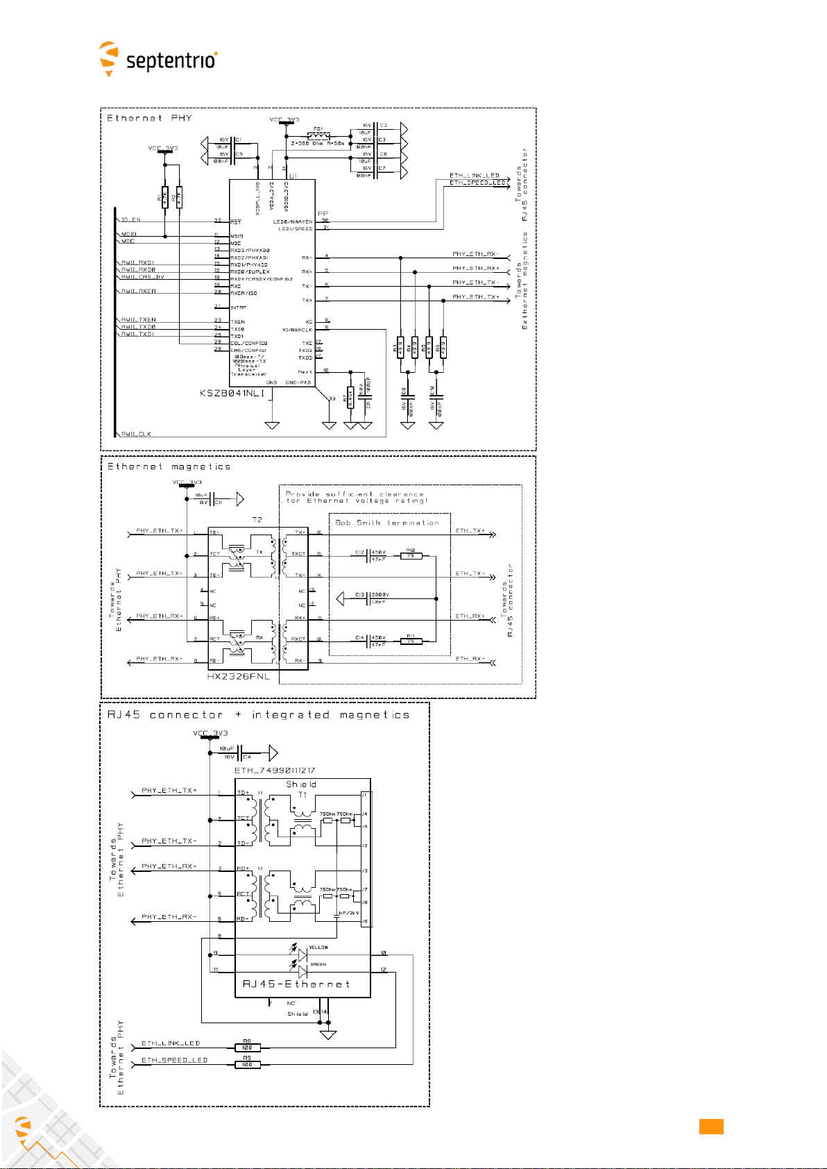
2.11 Ethernet
The receiver supports full duplex 10/100 Base-T Ethernet communication. The Ethernet
PHY and magnetics are to be implemented on the host board. Connection with the PHY
is through the RMII interface available on the 60-pin connector.
An example of application circuit is given in the next page. Two options are shown: stand-
alone magnetics or magnetics integrated in a RJ45 connector.
19
19
AsteRx-i OEM GNSS Module
19
Towards
OEM module

20
20
SBG Ellipse2 Micro
20
3SBG Ellipse2 Micro
3.1 Dimensions
All dimensions in mm. The IMU reference point is marked by the symbol.
This manual suits for next models
1
Table of contents
Other SEPTENTRIO Control Unit manuals


Popular Control Unit manuals by other brands

Nice
Nice Moon MC824H Instructions and warnings for installation and use

Siemens
Siemens 2AO U HF manual

Viessmann
Viessmann Vitovolt 300 Installation and service instructions

BENDIX
BENDIX SS-1 SHUT OFF VALVE manual

MIX
MIX SSM250 Series Operation and instruction manual

Polaris
Polaris Sync 3 Installation and user manual


