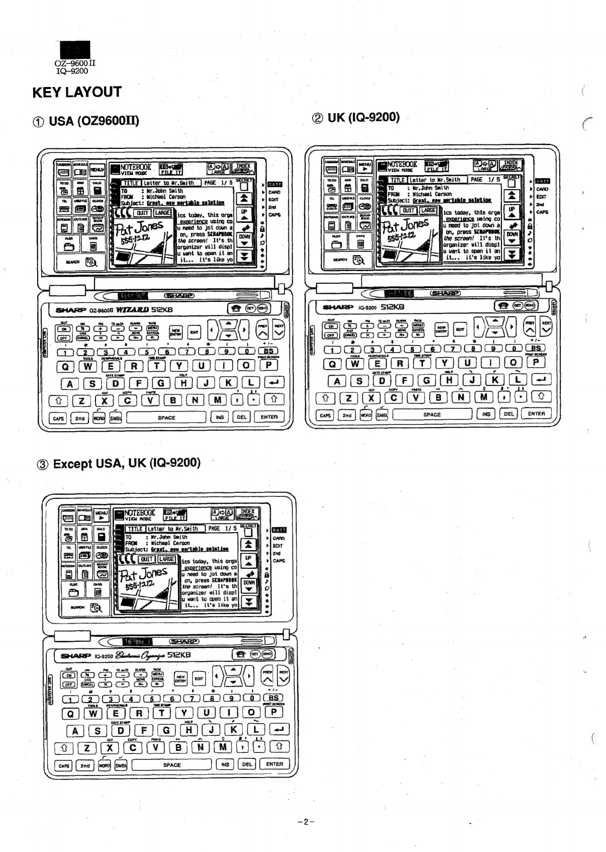
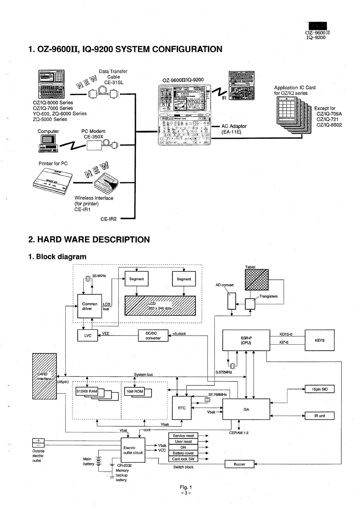
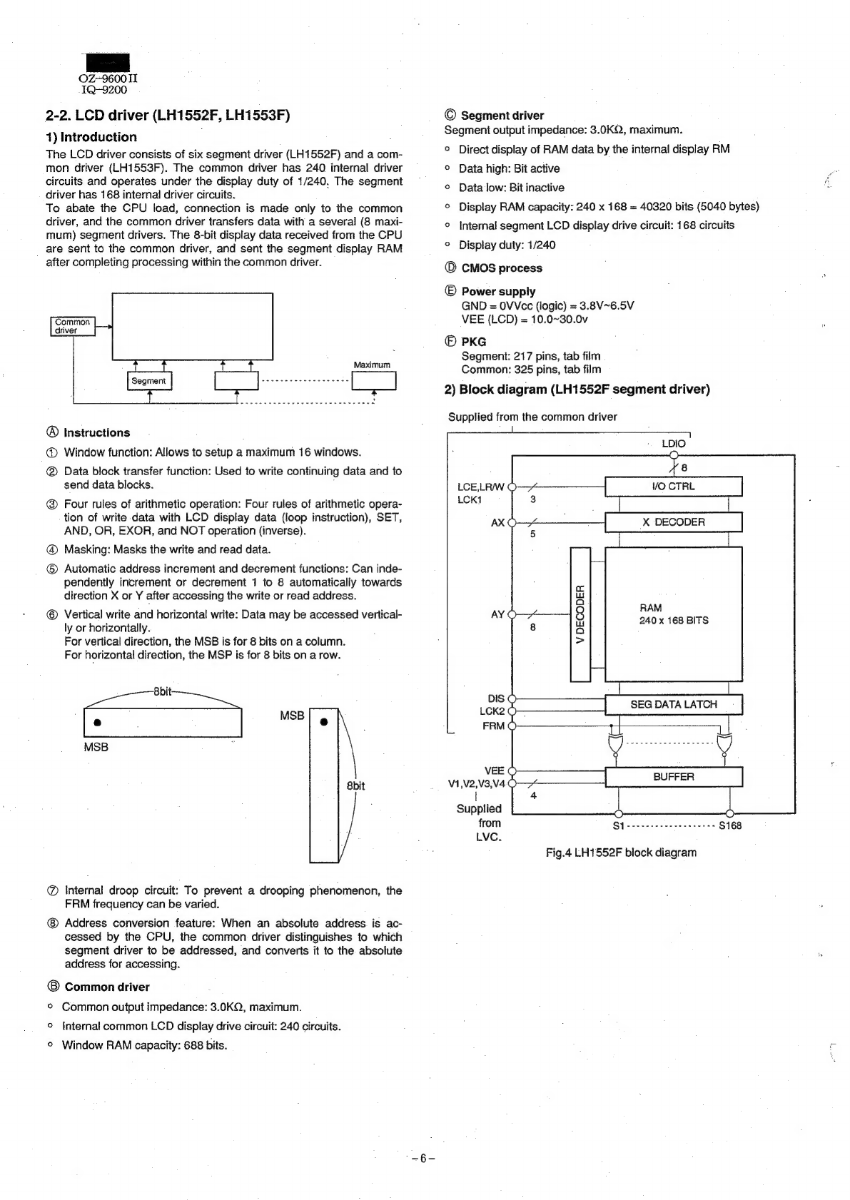
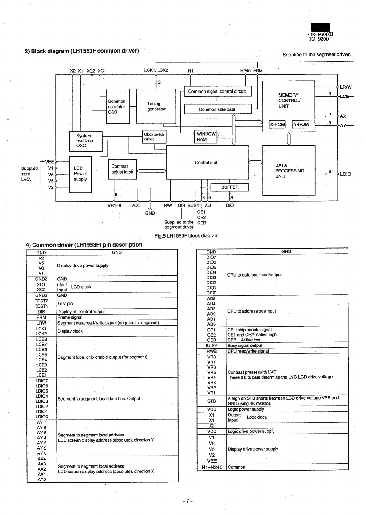
Sharp OZ-9600II User manual

OZ-9600
II
IQ-9200
SHARP
SERVICE
MANUAL
STANDARD
FUNCTION
10
digits
1M
DISPLAY SECTION
ELEMENT:
DISPLAY:
FSTN
LCD
320
x
240
dot
matrix
liquid
crystal
display
LSI
CPU:
LH58061M
Display:
LF7713Q
RTC:
SMC5245
POWER
SUPPLY
AG:X
DC:O
Main
power
supply:
6
Vde
Alkaline
batteries
(LRO3
x
4)
Memory
backup
power:
3
Vdc
lithium
battery
(CR2032
x
1)
POWER
CONSUMPTION
0.31
W
AUTO
POWER
OFF
TIME
12
minutes
MEMORY
PROTECT
Yes
DIMENSIONS(mm)
Open:
=
180(W)
x
210(D)
x
14.2(H)
mm.
7-3/32"(W)
x
8-9/32"(D)
x
9/16"(H)
Closed:
180(W)
x
105(D)
x
25.4(H)
mm.
7-3/32"(W)
x
4-1/8"(D)
x
1"(H)
Weight
Approx.
430g
CALCULATIONS
Functions:
addition,
subtraction,
multiplication,
division;
constant,
square
root,
percent,
memory
calculation,
date
calculation,
paperless
printer.
Digits:
10
digits
Serial
input/output
Type
of
transmission:
Asynchronoushalf-duplex/fullduplex
Transmission
speed:
300,
600,
1200, 2400,
4800,
9600
bps
Parity
bit:
even,
odd,
none
Word
length:
7
or
8
bits
Stop
bit:
1
or
2
bits
Connector
used:
15-pin
connector
Output
signal
level:
©
C-MOS
level
(4
to
6
volts)
Interface
signals:
Input;
RD,
CS,
CD, DR,
CI
Output;
SD,RS,
RR,
ER
Other;
.SG,
VC,
FG
Operating
temperatures
0°C
to
40°C
(32°
to
104°F)
Peripherals
and
transfer
interface
IR
transfer
Up
to
a
distance
of
approx.
80
cm.
Cable
jack
15-pin
IC
card
slot
1
Parts
marked
with
"A\”
is
important
for
maintaining
the
safety
of
the
set.
Be
sure
to
replace
these
parts
with
specified
ones
for
maintaining
the
safety
and
performance
of
the
set.
SHARP
CORPORATION
CODE:
00Z0Z96002SME
OZ-9600II
mopeL
1Q-9200
Electronic
Organizer
notebook
section
.
Applications
Calendar,
Schedule,
To
Do,
Anniversary,
Telephone,
User
File,
Notebook,
Outline,
Scrapbook,
Filter
Memory
capacity
512
Kbytes
(User
area:
Approx.
381
Kbytes)
Schedule
application
capacity:
:
Approx.
6,730
entries
consisting
of
an
averge
of
32
charactes
Tel
application
capacity:
Approx.
6,610
entries
consisting
on
averge
of
16
charactes
in
the
name
field
and
12
in
the
number
field
These
capacities
only
apply
when
all
the
available
memory
is
committed
to
a
single
function.
Maximum
Notebook:
16
Kbytes
data
size
per
Outline:
32
Kbytes
for
an
entire
outline
entry
2
Kbytes
for
each
topic
Tel/User
File:
2
Kbytes
for
text
data
61.7
Kbytes
for
graphics
data
Other
applications:
2
Kbytes
User
interfaces
Touch
panel,
keyboard
Other
features
Secret
function,
data
transfer,
search
Clock
Crystal
oscillation
frequency:
32,768
Hz
Clock
precision:
Average
variance
per
day,
1.5
seconds
(at
25°C/77°F)
Content
of
displays:
year,
month,
day,
day
of
week,
hours,
minutes,
A.M./P.M.,
city
names
:
Time
system:
12-hour
and
24-hour
clock
World
clock
function:
Display
of
date
and
time
for
the
world’s
cities.
Enable/dis-
able
daylight
saving
time
display
function.
Operating
time
Battery
life
may
vary
depending
on
usage.
Operating
batteries:
When
alkaline
batteries
are
used:
@
Approx.
80
hours
(2.5
months
of
1
hour
continuous
use
per
day)
Continuous
display
at
an
ambient
temperature
of
20°C
(68°F)
©
Approx.
70
hours
(2
months
of
1
hour
continuous
use
per
day)
Searching
data
for
5
minutes
and
display
on
for
55
minutes
per
hour,
at
an
ambient
temperature
of
20°C
(68°F)
The
battery
life
may
be
shorter
than
the
above
when
manganese
batteries
are
used.
Memory
backup
battery:
:
Approx.
5
years
(regardless
of
the
condition
of
the
operating
batteries)
Accessories
Alkaline
batteries
(LRO3
x
4)
Lithium
batteries
CR2032
(installed)
Touch
pen,
Operation
manual,
protection
card
This
document
has
been
published
to
be
used
for
after
sales
service
only.
The
contents
are
subject
to
change
without
notice.

OZ-9600II
IQ-9200
KEY
LAYOUT
@
USA
(OZ960011)
®
UK
(IQ-9200)
.
19-9200
512KB
SS
5
J
ee
Sateee
ante
0
DO@MDaWMMMmmsas
(2oe)
ki
caress
0
G3
G2
G4
5
Cs)
GC
C2
Co
Cs).
ealicajesis
slealea|eaieale
eck
ccoftaleaieajesleatea
[eal
reay
HEH
MMOWHE|
|
wAebimmec
cc
qje
BAM
PMOMMAEM)
|
BoMmeMeawwoow@
(a)
(i)
fo
i)
(ase)
(oe)
(Hm)
Caen)
(Ces)
Ce)
fe)
oo]
se)
C8)
Ga)
Cee)
@
Except
USA,
UK
(IQ-9200)
sual
FHTILE
[letter
to
wr.sith
]
PAGE
1/5
FROM:
:
Michael
Carson
»
Ar
4
;
:
LARGE!
f
.
H_exnertence
{
=a
ae
|
BSSSS8
GUA
282388
BA
Ualee
miwteytm)
wm
wCiejtr)
DSM
mmMMng
je)
MAD
OMB
was
(wes)
(a)
fos)
fa}
(ace)
8)
(ea)
Come)

OZ-9600
IT
TQ-9200
1.
OZ-9600II,
1Q-9200
SYSTEM
CONFIGURATION
Data
Transfer
Cable
CE-315L
OZ/1Q-8000
Series
OZ/AQ-7000
Series
YO-600,
ZQ-6000
Series
ZQ-5000
Series
Computer
PC
Modem
CE-350X
ate
Wireless
Interface
(for
printer)
CE-IR1
CE-IR2
2.
HARD
WARE
DESCRIPTION
1.
Block
diagram
Cee
ee
ee
ee
eee
ee
driver
System
bus
=e.
Application
IC
Card
for
OZ/IQ
series
Except
for
OZ/1Q-709A
OZ/NQ-721
ijmane
AC
Adaptor
OZ/1Q-8B02
(EA-11E)
converter
eee
ee
er
om)
Tablet
eeetetetetetee
<<
%
.¢,
£55054
>
Oo
Q
°
3
<
a
a
SOL
ESRP
(CPU)
KO15-0
KI7-0
ere
Ur
3.072MHz
:
RTC
Ew
Outside
outlet
circuit
electric
.
outlet
a
battery
-ss-
CR-2032
-Memory
‘3
backup
battery
CERAM
1-2
User
reset
Battery
cover
Card
lock
SW
Switch
block
Fig.
1
-3-

OZ-9600
IT
IQ-9200
2.
Description
of
LSI
2-1.
CPU
(LH58061M)
1)
Introduction
@
CMOS
process
@®
8-bit
CPU
(operand
at
8
bits)
@
Firmware
ROM
(decoder)
@
240
bytes
RAM
®
WO
port
(Input)
Key
input
System
control
input
CMT
input
UART
input
General
purpose
input
port
Key
output
Address
output
Chi
enable
output
LCD
driver
control
output
Memory
control
output
(Output)
2)
Block
diagram
wadoosa
yaauo-
Sub-clock
output
CMT
output
UART
output
General
purpose
output
port
Data
input/output
Power
supply
line
Oscillator
line
(input/output)
(Others)
;
©
Internal
circuit
Oscillator
circuitMain,
subsidiary
(for
timer)x2
Reset
circuit
:
UART
,
@
Supply
voltage3.8V~6.0V
Operating
temperature
range-5~55°C
@®
Not
the
bit
slice
microprocessor.
No
arithmetic
function
for
data
above
8
bits.
@
No
multiply
instruction
capability.
@
Does
not
contain
ROM
type
internal
memory
ROM.
®
100-pin
TQFP
(flat
plastic
package)
@
No
radiation
protective
design
provided.
°
TXD
-
@D
X4
X3
CEO
-----------
a a
CE
CONTROL
‘|
DIVIDER
suBosc
|:
INTERRUPT
CONTROL
YSdIAId
LI
RESET
TEST
ON
LHCTRL
Cl
CO
(240Byte)
43aqoo3a
yaauo-d
ees
py
-ORDER
DECODER
REGISTER
CONTROL
REGISTER
\S
Fee
p-ORDER
DECODER
m
MRQ
WR
REGISTER
|
CONTROL
JOYLNOO
ASIGOW
SSSYUGdV
LJ
voD
DIOO
----
DIO7
GND
Fig.2
LH5806AM
block
diagram
TOULNOO
UNVE
uasung
ssaucay
Y3445N@
LHOd-3
x
x
x
a
POWMOAAH
«x
«OK
PES
CJA20

3)
Pin
layout
582
Qqag2
WR
H
H
!
Reset
input
(PD)
OZ-9600
II
IQ-9200
4)
Pin
assignment
RSPR
eyet
.
CPU
signal
Circuit
signal
;
;
Pao,
|
name
|
name
|
YO
|
ALOFF
7~27
A0-A20
A0-A20
fe)
|
28.29
|
CEO.CE1
EXCED,CEIN
|__O
H
p85
ce?
cer
|
[Card
ROM
select,
system
ROM
select
|
p88
eS
CES
Card
RAMselect2
pe
Oe
ll
=
BS
OER
pO.
tM
a
ee
gies
cd
Ma
ROMOR:
ea
a
es
ps2
ee
tc
JPeripheral
vO
select
oo
88
ORS
=
CES
On
A
ee
RAM
OGD
es
|
p87
PD
control
clock,
4oKHz
|
39,40
|
x8,
x4
|
XR
X4
OT
OT
[CT
Forsub-logicosciliation
[|
CH
[Keyinputsignal
(PD)
|
__49~64
|
KOO-KOIS
|
KOO-KOIS
|
O_
|
L
a
ee
ee
or
he
re
hoor
EEO.
=
wy
=
PERO
|
Oro
cbt
de
oe
he
kl
oh
jo
OO
BED
NG
0
eh
ee
Noted
poe
Ofte
2
|e
EE
=
NO
ee
Ms
INetee
=
p68
TEST
ta
|
[ECD
timingsignal,
MHz
peo
ON
ON
Okey
input
interrupt
fo
TxD
TsO
oT
sorr
fT
SOFT
TH
iSpinsenddata
Pmt
tS
pinrecevedata
p72
|
EO
SELECT
|
O__|
Notpredictable
[Notpredictable["
“SOFT
|
H_
[ForiSpin
poo
ES
A
Ne
ee
NOR
p74
ER
S20
_[
Notpredictable
|
Notpredictable
|
SOFT
|
_H__|Cardrecognition
strobe
output
|
75
|
ES
|
ROMBANK
|
O__[
Notpredictable
|
Notpredictable|
SOFT
|
=H
[ROMbankmain
pe
TAT
tRMO
TT
Tittertupt
signalirom
ATC
77
ES
TBINT
-—-}
|_|
fee
ee
ag
78
E6
UNLOCK
PC
Lock
switch
interruptsignal
PO
Et
=
NU
ee
ee
[Not
ap
__E8
RS
—
SOFT
Not
predictable
81
EQ
ER
SOFT
Notpredictable[
SOFT
|
H_[Fori5pin,
82
E10
cD
bot
in
et
eee
Se
ODIO
<=
ae
=
oe
pe
83
E11
DR
fe
ee
eee
hee
OPIN
ee
E12
cTs
fic
a
es
PROS
DID
oe
gn
a
ened
85
E13
Bello
of
tf
|
CTC
tS
pinstartupinput
E14
NU
ee
ae
re
SOFT
|
Notpredictable|"
SOFT
[
H
[Cardoutputenable
[|
CC*dT:
Ss
Forsystemclock
oscillation
For
LCD
control
(not
used)
Test
pin
(GND
connected)
Card
recognition
external
PD
Beeper
output
signal
Memory
1/O
write
pulse
Memory
request
(not.
used)
:
i
xy
c-yx
Reference
voltage
No
backup
power
supply,
VCC

OZ-9600
IT
TQ-9200
2-2.
LCD
driver
(LH1552F,
LH1553F)
1)
Introduction
The
LCD
driver
consists
of
six
segment
driver
(LH1552F)
and
a
com-
mon
driver
(LH1553F).
The
common
driver
has
240
internal
driver
circuits
and
operates
under
the
display
duty
of
1/240,
The
segment
driver
has
168
internal
driver
circuits.
To
abate
the
CPU
load,
connection
is
made
only
to
the
common
driver,
and
the
common
driver
transfers
data
with
a
several
(8
maxi-
mum)
segment
drivers.
The
8-bit
display
data
received
from
the
CPU
are
sent
to
the
common
driver,
and
sent
the
segment
display
RAM
"after
completing
processing
within
the
common
driver.
Common
driver
Maximum
®
Instructions
@
Window
function:
Allows
to
setup
a
maximum
16
windows.
@®
Data
block
transfer
function:
Used
to
write
continuing
data
and
to
send
data
blocks.
@®
Four
rules
of
arithmetic
operation:
Four
rules
of
arithmetic
opera-
tion
of
write
data
with
LCD
display
data
(loop
instruction),
SET,
AND,
OR,
EXOR,
and
NOT
operation
(inverse).
@
Masking:
Masks
the
write
and
read
data.
©
Automatic
address
increment
and
decrement
functions:
Can
inde-
pendently
increment
or
decrement
1
to
8
automatically
towards
direction
X
or
Y
after
accessing
the
write
or
read
address.
©
Vertical
write
and
horizontal
write:
Data
may
be
accessed
vertical-
ly
or
horizontally.
For
vertical
direction,
the
MSB
is
for
8
bits
on
a
column.
For
horizontal
direction,
the
MSP
is
for
8
bits
on
a
row.
8bit
MSB
MSB
8bit
@
Internal
droop
circuit:
To
prevent
a
drooping
phenomenon,
the
FRM
frequency
can
be
varied.
Address
conversion
feature:
When
an
absolute
address
is
ac-
cessed
by
the
CPU,
the
common
driver
distinguishes
to
which
segment
driver
to
be
addressed,
and
converts
it
to
the
absolute
address
for
accessing.
Common
driver
©
Common
output
impedance:
3.0KQ,
maximum.
©
Internal
common
LCD
display
drive
circuit:
240
circuits.
©
Window
RAM
capacity:
688
bits.
©
Segment
driver
Segment
output
impedance:
3.0KQ,
maximum.
o
°
°
°
°
°
Direct
display
of
RAM
data
by
the
internal
display
RM
Data
high:
Bit
active
Data
low:
Bit
inactive
Display
RAM
capacity:
240
x
168
=
40320
bits
(5040
bytes)
Internal
segment
LCD
display
drive
circuit:
168
circuits
Display
duty:
1/240
©
CMOS
process
©
Power
supply
GND
=
0VVec
(logic)
=
3.8V~6.5V
VEE
(LCD)
=
10.0~30.0v
©
PKG
Segment:
217
pins,
tab
film
Common:
325
pins,
tab
film
2)
Block
diagram
(LH1552F
segment
driver)
Supplied
from
the
common
driver
RAM
240
x
168
BITS
oO
uu
Qa
8
uu
Qa
>
v1
v2,V3,v4
04+}
I
Supplied
from
ou
deke
ooseetaeosas
ee
68
LVC.
Fig.4
LH1552F
block
diagram

OZ-9600
IQ-9200
3)
Block
diagram
(LH1553F
common
driver)
é
sau
if
Pee
:
upplied
to
the
seg
river.
X2
Xt
XC2
XCi
LCK1,
LCK2
Hasitest
i
cserset
secs
H240
FRM
MEMORY
a
CONTROL
Timing
UNIT
generator
a
oscillator
[-—
Osc
Control
unit
Supplied
Contrast
;
from
adjust
latch
PROCESSING
.
ee
LVC.
UNIT
r
BUFFER
VR1~8
vcc
RW
DIS
BUSY:
AD
DIO
;
GND
|
CE
CE2
Supplied
tothe
CEB
segment
driver
Fig.5
LH1553F
block
diagram
4)
Common
driver
(LH1553F)
pin
description
V2
ve
Display
drive
power
supply
v1
PGND2
|
xC1
utput
XC2
Input
LCD
clock
GND3__
[GND
TEST?
ley
TESTI
Stpin
Display
off
control
output
FRM
LRW
Segment
data
read/write
signal
(segment
to
segment)
LCK1
:
LOKe
Display
clock
CPU
to
data
bus
input/output
CPU
to
address
bus
input
CE1
CPU
chip
enable
signal
CE2
CE1
and
CE2:
Active
high
CEB
CEB,
Active
low
BUSY
Busy
signal
output
CPU
read/write
signal
cr
m
fe)
Segment
local
chip
enable
output
(for
segment)
Contrast
preset
(with
LVC)
These
8
bits
data
determine
the
LVC
LCD
drive
voltage.
STB
A
high
on
STB
shorts
between
LCD
drive
voltage
VEE
and
GND
using
3K
resistor.
Logic
power
supply
x1
Output
;
X41
Input
Lock
clock
:
X2
ane
Segment
to
segment
local
data
bus:
Output
:
Segment
to
segment
local
address
AY3
LCD
screen
display
address
(absolute),
direction
Y
AX3
AX2
Segment
to
segment
local
address
LCD
screen
display
address
(absolute),
direction
X

OZ-9600IT
TQ-9200
5)
Segment
drive
(LH1552F)
pin
description
-
6)
LCD
driver
waveforms
Signal
+4.
a
vE
8
20~28V
1~168
|
S1~S168
[Segment
output
VO:
oe
peters
;
Display
GND
V4---++
Lope
sess
eee
eee
eee
ee
—
Segment
waveform
ee
Common
waveform
et
SnD
FRM=1
FRM=0
wy
Display
drive
power
supply
SEGMENT
175
VEE
_ |
Display
drive
power
supply
GND
Logic
drive
power
supply
Common
to
common
local
address
179
AX1
180
AX2
LCD
screen
display
address
181
AX3
|
Direction
X
(absolute)
182
AX4
183
AYO
Common
to
common
local
address
COMMON
Input
|
FRM
|
Level
184
AY1
1
1
v2
185
AY2
LCD
screen
display
address
0
1
V6
186
AY3
Direction
Y
(absolute)
1
0
Vi
187
AY4
188
AY5
: 2
ve
189
AY6
190
AY7
191
LDI07
[Common
to
common
local
data
bus
192
LDIO6
=|
input/output
2-3.
RTC
(SMC5245)
193
LDIO5
.
194
LDIO4
1)
Pin
layout
195
LDIO3
eke
BES
eng
nN
=
MUO
uy
Wu
rs
uw
use
ae
SOR
CELSS
ESSE
LCE
200
LCK1
201
LCK2
Segment
data
read/write
signal
(common
to
LRW
common)
:
Frame
signal
DIS
Display
off
control
input
MIRROR
|
Mirror
reflect
input
206
TEST1
207
|
TEST2
|Testpin
208
GND
|GND
iad
ancl
209
VCC
__
|Logic
drive
power
supply
GND
|GND
;
Display
drive
power
supply
Local
to
local,
local
chip
enable
input
Display
clock
(common
to
common)
Display
drive
power
supply
isp]
onrN
BHEaARBE
>Hooo
a
Fig.6
SMC5245
pin
layout
Display
drive
power
supply
GND

2)
Pin
description
Function
RW
NC
AO
At
A2
A3
A4
Do
DI
D2
D3
D4
D5
NC
D6
D7:
ALARM
INSRES
VDETO
.
SRES
ON
OCE2
OCE1
OCEO
SCE
NC
BTCOV
RSKEY
ONKEY
ICE2
VSS
—
o0o0o0o000
0-0
Supply
voltage
Not
used.
Not
used.
|
Reset
terminal
Crystal
oscillator
connect
pin
.
Crystal
oscillator
connect
pin
‘|
Not
used.
Internal
low
voltage
output
regulation
capacity
connect
pin
Frequency
output
pin
Voltage
monitor
pin
Voltage
monitor
pin
Voltage
monitor
pin
Voltage
monitor
pin
Test
pin
Chip
select
pin
Chip
select
pin
Chip
select
pin
Read/write
pin
Not
used.
Address
bus
Address
bus
Address
bus
Address
bus
Address
bus
Data
bus
Data
bus
Data
bus
Data
bus
Data
bus
Data
bus
Not
used.
Data
bus
Data
bus
Interrupt
output
pin
Reset
input
pin
VDD
output
monitor
pin
Reset
output
pin
ON
key
output
pin
WR
output
pin
|
‘Not
used.
Not
used.
©
D
battery
protection
control
pin
Not
used.
Battery
replace
pin
Reset
switch
|
ON
key
input
pin
WR
input
pin
Power
supply
OZ-9600
II
IQ-9200
3)
Introduction
The
SMC5245
is
a
calendar
combined
real
time
clock.
It
has
a
basic
frequency
of
32,768Hz
generated
from
a
crystal
oscillator
to
produce
second,
minute,
hour,
day,
day
of
week,
month,
and
year.
It
has
an
automatic
leap
year
interrogating
feature
of
the
world
calendar,
cyclic
interrupt
feature,
2-channel
alarm
feature,
and
a
4-channel
external
voltage
detect
feature.
For
interfacing
with
a
microcomputer,
it
uses
8-bit
data
bus,
5-bit
address
bus,
3-bit
chip
select
and
read/write
signals,
allowing
to
set
time,
alarm,
interrupt
and
to
read
time,
interrupt
cause,
and
voltage
detect
result.
A
part
of
the
oscillation
circuit
and
the
frequency
divider
are
driven
by
a
low
voltage
for
a
low
power
consumption.
4)
Features
@
High
speed
CPU
interface
by
means
of
8-bit
data
bus.
*
©
Internal
time
counter
(second,
minute,
hour)
and
calendar
(day,
day
of
week,
month,
year).
®
internal
automatic
leap
year
recognition
feature
@
internal
2-channel
alarm
feature
with
a
wild
card
feature
©
Internal
cyclic
interrupt
feature
(day,
hour,
minute,
second,
1/2
second)
©
Internal
4-channel
external
voltage
detect
circuit
@
Low
power
dissipation
using
the
CMOS
technology
and
the
volt-
age
regulator
Internal
32.768Hz
crystal
oscillator
5)
Pin
functions
@
D0~D7:
8-bit
data
bus
These
are
bidirectional
data
bus
that
connected
with
the
microcomputer
data
bus
and
used
to
read/write
counters
and
registers.
The
data
bus
is
at
a
high
impedance
except
when
CS0~CS2
is
active
and
R/W
is
at
a
high.
@
A0~A4:
5-bit
address
bus
These
are
address
input
lines
that
are
within
the
microcomputer
address
bus
and
used
to
assign
read/write
counters
and
registers.
@
CS0~CSS5:
5-bit
address
bus
These
are
chip
select
lines
used
to
set
active
and
inactive
the
IC.
Normally,
address
decoded
signal
is
connected.
CSO
is
an
active
low
signal.
CS1
and
CS2
are
active
high
or
low
that
can
be
selected
by
masking.
The
IC
becomes
active
when
the
3-bit
select
line
has
turned
active.
®
Read/Write
pin
The
contents
of
the
counter
and
the
register
designated
in
ad-
dress
AO~A4
at
HIGH
level
are
outputted
to
the
data
bus.
Writing
is
performed’
at
LOW
level.
When
CS0~CS2
are
non-active,
neither
read
nor
write
can
be
made.
©
ALARM
interrupt
output
pin
—
Cyclic
interrupt,
alarm
interrupt,
and
voltage
detect
interrupt
are
informed
to
the
external
source.
With
a
mask
option,
active
low
or
high
state
can
be
selected.
Only
the
software
can
be
assigned
to
set
this
line
for
set
active
or
anaenve:
These
lines
are
not
affected
by
CS0~CS2.
©
FOUR
frequency
output
pin
The
frequency
of
32Hz
is
sent
onto
this
output
line
for
step
adjust-
ment
of
the
clock.
@
OSC1,
OSCO
crystal
oscillator
connect
pin
These
are
pins
connected
with
the
32,768
crystal
oscillator.
®
VDO0~VD3
detect
voltage
pin
These
are
input
lines
used
to
monitor
external
voltage.
@
Pin
numbers
2,
3,
35~48
(QFP,
48
pins)
user
circuit
i/o
pins
input/output
pins
used
for
the
user
circuit.
@
VDD,
VSS
power
supply
pin
These
lines
are
used
to
supply
power.
@
VREG
internal
low
voltage
output
regulation
capacitor
connect
pin
A
0.1
capacitor
is
connected
across
VREG
and
VSS.

OZ-9600
IT
TQ-9200
@®
RESET
reset
pin
This
line
is
used
to
initialize
the
IC.
A
high
on
this
line
initializes
all
register
contents.
In
addition
to
this
function,
it
also
has
an
internal
power-on-reset
circuit.
The
reset
is
OR’ed
with
the
power-on-reset
circuit.
Internal
pulldown
is
not
provided
on
the
reset
line.
NOTE:
The
power-on-reset
circuit
may
not
start
active
depending
on
how
the
power
is
turned
on.
@®
TEST
test
pin
Only
Seiko
Epson
may
provide
it
for
test
of
the
IC.
Normally,
it
is
internally
pulled
down.
It
is
suggested
to
connect
with
VSS
exter-
nally.
6)
User
circuit
The
user
circuit
consists
of
14
input/output
lines.
ONKEY,
RSKEY,
and
BTCOV
lines
are
Schmitt
trigger
inputs
that
normally
pulled
down
internally.
The
one-shot
circuit
issues
a
high
level
signal
(normally
low)
to
the
8/512~9/512
one-shot
circuit
at
a
high
to
low
transition
of
the
BTCOV
line.
The
one-shot
circuit
has
a
trigger.
The
one-shot
circuit
output-2
has
a
delay
of
1/2024~3.1024
second
and
continues
to
sent
high
level
until
the
BTCOV
line
becomes
high
(normally
low).
The
VDA
signal
is
an
output
from
the
voltage
detector
A.
A
high
level
signal
is
issued
when
normal
(voltage
found).
This
signal
is
at
a
high
at
a
time
of
initialization.
The
NADOCW
signal
is
an
active
low
ad-
dress
0CH
write
signal.
The
DFR
signal
is
a
register
of
a
user
bit
that
sends
the
input
level
of
D
to
Q
at
a
low
to
high
transition
of
signal.
When
a
low
level
signal
is
received
by
R,
the
DFR
is
reset
with
a
low
level
signal
sent
to
Q.
(XQ
is
an
invert
output
of
Q).
0G
NADOCH
INSRES
7
ake
2212
VDA
eee
{>
7
ICEO
faq)
ze
Pipst
1CEA
21
Ay
7
3iN2
Se
>
2nc4
1
1.—3
1
Ice
1
22%
—~o2
2)
TR
o22,
St?
1.—3
we
ONKEY
oe
Ij)
1S
e
13
3
RSKEY
241
2]
)
;
Be:
tho!
ee
‘
ae
2
i)
4
BTCOV
2
fo
22
ie
onesHor
|
2-4.
System
gate
array
(LZ95G33)
1)
Brief
functional
description
@
Memory
decode
‘
Used
to
decode
the
system
ROM,
RAM,
and
IC
card
memories
that
produces
a
chip
select
signal
for
each
assigned
device.
@
Write
pad
interface
Has
an
interface
circuitry
with
the
handwrite
pad.
@
Optical
communication
interface
Not
only
switches
the
CPU
serial
port
to
a
normal
15-pin
port
from
the
optical
communication,
it
also
modules
the
optical
communica-
tion.
;
@
CDROM
interface
Not
only
switches
the
normal
serial
port
from
the
CDROM,
it
also
switches
the
CDROM
drive,
and
it
controls
the
communication
with
the
CDROM
drive.
©
Tablet
conirol
Used
to
control
the
tablet
input
and
the’
A/D
converter.
©
Memory
protect
The
memory
is
protected
using
an
external
voltage
detect
IC.
OCE1
SRES
VDETO
-10-
@
EEPROM
control
Used.
to
control
the
EEPROM
access,
and
has
a-function
to
replace
a
part
of
ROM
to
a
part
of
the
EEPROM.
Used
to
generate
clocks
and
low
battery
signal
cut
out
function.

OZ-9600
IT
I1Q-9200
2)
Block
diagram
CEG6N
CE80N
Rate
eral
ae
CE8iN
SD
es
15-pin
serial
;
TXD
_-
ROM
Mapper
-1_orepn
paxp—e
contrel:
2
fa
ap
EXROMN
RTS
aa
RS
:
15-pin
control
:
———
CTS
CESN:
: 3
. :
:
:
OPTS
(Light:
transmit)
'
CERAM1
:
Optical
serial
ae
|
‘
*
OPTR
(Light:
receive)
-
Pe
——
CERAM2
'
:
4
CE1N
:
Power
supply
:
PB20N
A17N
a
;
control
bs
CE8N
=
RAM
Mapper
;
CE2
|
EXRM1N
|
|
CES.
EXAM
us
|
1
XMONN
1
———
CSZ80N
‘
——
YMONN
1
Z80BUS
|
—
SWXL
ADRDN
|
Tablet
control
ti
sw
LCD
1/0
Mapper
:
transistor.1/O
“4
ADWRN
|
MON
Ly.
ADCSN
|
—
SWXHN
oe
See
ea
1
internal
I/O
selectio
SWYHN
L1
SwaN
2\.
Vbak
SS
:
;
GND
=
Booster
circuit
1
CRCLK
1;
||
contro!
output
Eeners
D/A
conversion
control
‘7
:
ALARM,
Cl
control
(DA5-0)
:
ae
DAWRN
BELLI,
BELLO
se
Bs
PCIO,
PCOO
Operation/stop
‘4
control
circuit
BSY
EEPROM
control
1
EPRESN
:
SEPAI2-8.
CLK
u
UNLOCK
L-—
Ms
fee
ee
eB
a
a
the
a
GN
Ne
er
ee
el
te
Mek
gs
ad
Fig.7
LZ95G33
block
diagram
-11-

OZ-9600
11
1Q-9200
3)
Pin
description
[FINN
|
Signal
name
|
1
cs
Description
[Chip
Select]
=
a
Chip
select
signal
input.
A
low
on
this
line
accepts
WR
and RD.
[Read]
Daia
read
signal
input.
A
low
on
this line
send
the
conversion
data.
Pee
—_—
|[Write]
[a
3
WR
Goes
into
the
standby
mode
with
-CS
at
a
low
and
-WR
at
a
low.Data
write
signal
input
that
the
data
is
read
at
a
low
F
to
high
transition
and
starts
the
conversion.
=
:
pm
id
[Clock
Onput}
Standard
clock
input
for
conversion.
;
[Interrupt](Not
used)
'
-INTR
Conversion
termination
signal..Goes
into
a
low
state
after
completion
of
conversion,
and
returns
to
a
high
state
with
a
first
-RD-
signal
and
a
high
state
of
-WD
signal.
;
,
poo
ie
,
[cs]
fe
-
VINA
Analog
input
line.
Input
range
is
GND~VREF.
ON
onaane!
__VIN4
AGND
[Analog
Ground]
: :
;
f
Reference
voltage
supply
line
that
determines
the
zero point
of
VIN.
Pon
:
VREF
[Reference
Voltage]
Reference
voltage
supply
line
that
determines
the
full
scale
point
of
VIN.
BIT1
[Data
Output]
Conversion
data
output
line.
[Digital
Ground}
System
ground
line,
normally
at
0.0V.
10~2
turn
into
the
input
mode
according
to
the
mode,
and
the
channel
select
(CHS)
and
output
control
data
(BUSC,
OUTC)
are
written.
Remote
mode
(RD="L’):
Conversion
data
are
sent
from
bits
0~9
according
to
the
output
contro!
signals
(BUSC,
OUTC).
BIT3/11
/
20
|
eireno
[Mode]
:
|
a1
|
Mop
Used
to
assign
the
data
write
mode
(10~2).Mode="L":
10
input
mode,
mode="H":
10~2
input
mode.
(NC)
[No
Connection]
ve
é
BITO:LSB
BIT9:MSB
Reference
clock
voltage
output
line
for
conversion.
[Power
Supply]
.
Power
supply
line:
5.0V10%.
=14-

2-7.
EEPROM
(uPD28C64GX)
-
1)
Functional
description
The
»PD28C64GX
has
the
following
two
functions.
The
end
of
the
data
cycle
can
be
exactly
known
from
the
external
source,
and
it
may
also
shorten
the
write
time.
*
Data
poll
function
It
has
three
modes
to
kill
noise,
to
detect
the
Vcc
power
supply
level,
and
the
write
prohibit
logic.
*’
Write
error
prevent
function
@
Data.poll
function
With
the
data
poll
function,
the
exact
end
point
of
the
write
cycle
can
be
confirmed
software-wise.
Using
this
function,
the
control
can
move
to
a
next
write
cycle
immediately
after
the
present
write
cycle
has
ended.
The
maximum
value
of
the
pPD28C64GxX
write
cycle
time
is
set
to
12ms,
while
the
standard
value
at
the
end
of:the
write
cycle
is
7ms.
So,
the
write
time
can
be
reduced
if
this
data
poll
function
is
utilized.
‘Do
the
following
procedure
to
poll
data.
(a)
After
writing
the
data
in
the
uPD28C64GX
with
the
WE
con-
trol
write
signal,
the
signal
WE
is
retained
high
level
and
the
data
in
the
written
address
(in
the
page
write
mode,
the
last
;
written
address)
is
read
(refer
to
the
read
mode
timing).
(b)
The
output
data
is
compared
with
the
written
data.
-
If
/O7
of
the.
output
data
is
verified
successfully
with
the
written
data,
the
write
operation
is
finished.
Now,
you
can
proceed
to
a
next
write
cycle.
If
the
write
was
not
completed,
-
the
inversion
of
the
write
data
are
sent
and
"0"
is
sent
to
all
bits
through
1/00~1/O6.
NOTE:
Refer
to
the
2-operation
mode
for
the
WE
control
write
mode
and
the
page
write
mode.
Example)
If
the
write
data
was
"10101010,"
the
output
data
will
be
"10101010"
when
the
write
has
been
completed.
If
not
completed,
the
output
data
will
be
"00000000".
Last
data
write
”
Write
completion
)
a
cas
|
‘CE
(input)
PRIN
EN
GE
(input)
=
Ne
Ser
WE
(input)
VO7.
cS
ee)
Swerigr
(Output)
(Output)
-
(Output)
i
ad
a
eoie
"yb
seb
sry
a
as
Lyon
l
fei
A0~A14
(input/output)
—
NOTE:
The
broken
liné
represents
an
high
impedance
state.
+n”
represents
an
address-n.
@®
Write
error
prevention
function
The
pPD28C64GX
has
the
following
three.
modes
to
prevent
data
-
_
Write
error,
a,
sgh
(a):
‘Noise.
pesventon:
Sorgen
es).
.Write.is
prohibited
if
the
WE
pulse
i
is
cinder
15ns.
by
Supply
voltage
Vcc
level
detect
function
Write
i
is
Prohibited
if
the
power
supply
voltage
is
under
2.5V.
Rete
_
Write
prohibit
logic
.-
“
Write
is:
prohibited
if
OE="VIL"
OF.
.
WE="VIH",
or
CE="VIH",
when
the
supply.
atege!
is
on
or.off..
Od
0Z-9600.11
IQ-9200
2)
Block
diagram
:
Data
input/output
~
vce
O———>
VO0~1/07
GND
O-——>
Write
enable
Output
enable
;
Chip
enable
Y-decoder
=>
/O
buffer
data
latch
Y-selection
256K-bit
©
X-decoder.
.
memory
cell
array
Address
buffer
address
latch
Fig.11
»PD28C64GX
block
diagram
'
3)
Pin
layout
~45—
1
2
3
4
5
6
7
8
pPD28C64GX
vO7
A10
0
Fig.12
pPD28C64GxX
pin
layout
4)
Pin
description
ce
—
—ceeonige
=
FOE
|
Output
enable
input
=|
WE
|
Wit
enabie
put
Vcc
Powersupply
fend
Inc
Not
connected
5)
Operation
mode
The
PD28C64GX
has
five
operation
modes.
For
all
modes,
set
-CE,
-OE-,
and
-WE
to
the
voltage
level
shown
in
Table
2-1.
The
pPD28C64GxX,
however,
leaves
the
factory
with
all
bits
"1"
canceled.
/00~V/07
Data
output
Seb
X
|
High
impedance
Vi
[Vit
[Data
input
VIHH
|
VIL
.
|Data
input
(DIH=VIH)
vie
|
ip
erase
|
viL_|
Ed
Ex
NOTE:
VIH:
High
level
input
voltage
VIHH:
+15V0.5V
VIL:
low
level
input
voltage
X:
VIL
or
VIH
Table
2-1.
Operation
modes

OZ-9600
II
1Q~-9200
@
Read
mode
Pe
LE
es
When
CE
and
OE
are
low,
it
goes
into
the
read
mode.
The
output
data
will
be
sent
onto
the
data
bus
through
the
data
i/o
lines
(VO0~I/O7)
with
an
address
data
output
delay
time
(tACC)
after
the
address
has
been
set,
or
with
an
data
output
delay
time
(tOE)
from
a
high
to
low
transition
of
OE.
@
Standby
mode
.
When
CE
is’set
to
a
high
state,
it
goes
into
the
standby
mode.
In
this
mode,
/O0~1/O7
turn
high
impedance
regardless
of
what
state
OE
is.
;
@®
Write
mode
(a)
Byte
write
mode
a
te
When
CE
and
WE
are
set
low
and
OE
high,
it
goes
into
the
write
mode.
it
is
possible
for
the
pPD28C64GxX
to
control
CE
and
WE.
Address
is
latched
at
a
high
to
low
transition
of
CE
or
WE
whichever
appeared
later.
The
data
is
latched
a
a
high
to
low
transition
appeared
earlier.
The.
automatic
erasure/write
completes
within
12ms
of
the
write
cycle
time
(tWC).
;
(b)
Page
write
mode
The
wPD28C64GX
allows
page
write
up
to
32
bytes
per
page.
Utilizing
this
feature,
all
bytes
will
be
completed
to
write
within
3
seconds.
The
»PD28C64GX
comprises
246
pages
x
32
bytes.
To
use
the
page
write
function,
the
page
is
assigned
through
the
address
A5~A12,
then
the
data
are
sequentially
written
through
the
address
AO~A4
or
may
be
written
at
random.
However,
unless
a
next
address
is
sent
within
100s
of
the
byte
load
cycle,
it
starts
the
internal
auto-
matic
erasure
or
write
operation.
No
page
can
be
changed
in
a
course
of
the
write
cycle.
:
@®
Chip
erase
mode
The
pPD28C64GxX
goes
into
the
chip
erase
mode
when
OE=VIHH
(15V0.5VO
and
CE=WEs="L".
In
this
occasion,
data
inputs
/00~1/07
must
be
set
to
high
level.
Address
input
is
“don’t
care”.
©
Write
inhibit
mode
When
OE
is
set
low
or
WE
is
set
high,
it
goes
into
the
write
inhibit
mode
and
disables
to
write
anything.
;
-16-
3.
Memory
mapping
Main
memory
|
CARD
~~
99000h
8000h
ee
Sra
oe
aT
|
eR
etc
ATC
iat
cpuvo)
|
beer
8100h
System
VO
pe
20000)
|
eee
eee
hee
,
3400h
|_—~Pohibited
area__|
Prohibited
area
CARD
RAM1
AM2N)
pe
ene
5
an
:
Touch
panel
8900h
=
secant
60000h
Prohibited
area
‘Touch
panel
(CERAM2)
Prohibited
area
80000h
CEIN
CE8N
A0000h
({CERAM1)
;
coooon
Seep
ieenugeteenpteias
cee
ceree
Ppoee
ete
ae
oe
ot
reer
CESIN
‘E3*CEBON™
E3*CESON
-
MEIN
GARD
ACTIVE
CEO
80000~BFFFF
L
CE1
80000~BFFFF
L
CE2
20000~3FFFF
H
CE3
NC
-
CE4
8000~8FFF
H
CE5
H
CE6
COOOO~FFFFF
L
CE7
40000~7FFFF°
L
4.
LCD
booster
circuit
To
drive
the
LCD,
the
power
is
generated
using
a
step-up
type
chop-
per
converter.
Its
operating
principle
is
explained
in
the
lines
to
follow.
vec
The
clock
of
approximately
30KHz
is
supplied
from
the
CPU
through
oD
that
can
be
controlled
to
supply
and
discontinue
‘to
the
converter
by
means
of
DF/F
output
of
the
gate
array.
©
is
set
high
in
a
course
of
starting
up
the
unit.to
supply
the
clock
to
the
converter.
©
is
set
low
in
a'course
of
quitting,
and
the
point
@
is
fixed
low.
As
the
operational
theory,
when
the
clock
is
supplied
to
®
with
the
point
®
at
a
high,
the
Q2
is
set
on/off
by
the
1C1
output.
Energy
is
stored
in
the
coil
L
during
the
Q2
on
period;
and
the
energy
is
released
during
the
Q2
off
period.
The
output
voltage
is
controlled
by
the
zener
diode
AD.
When
the
zener
voltage
goes
above
VBE
of
+Q1,
the
transistor
Q1
is
turned
active
with
the
point
B
set
low.
Until
the
output
voltage
drops,
the
point
©
is
kept
low
and
the
converter
discontinues
to
operate.
The
figure
on
the
next
page
shows
the
waveforms.
(In
terms
of
operation,
it
is
a
negative
feedback
that
VEE
becomes
stable.)

®
@
esr
es
Slash
os
te
A
pe
re
ee
ee
ae
Tera,
el
LeDon
Voltage
boosting
Voltage
decreasing
®@®@®@eod
VEE
I
LCD
off
x
Although
the
voltage
VCC-VF
is
added
to
VEE
while
the
unit
is
off,
no
voltage
is
added
to
the
LCD
driver
since
it
is
turned
off
within
LVC
(transistor
switched).
5.
Operation
of
the
transparent
tablet
(A/D
converter)
To
locate
the
point
on
the
transparent
tablet,
it
uses
a
tablet
control
transistor,
an
A/D
converter,
and
a
gate
array.
In
the
A/D
converter,
the
coordinates
X
and
Y
of
the
tablet
is
con-
verted
from
the
analog
voltage
to
a
10-bit
data.
(Conversion
is
done
after
checking
the
pressure
level
is
above
a
fixed
level.)
The
tablet
is
multiplexed
via
the
control
transistor,
and
voltage
is
added
towards
X
and
Y
axis.
A
voltage
proportionate
to
the
pressed
point
is
sent
to
YL
for
the
X-axis
and
XL
for
the
Y-axis.
The
gate
array
controls
the
A/D
converter
(read/write)
and
output
of
the
transistor.
To
save
power
consumption,
the
A/D
converter
is
kept
in
the
standby
mode
(CS
and
WR
forcing
low)
and
the
reference
voltage
for
the
A/D
converter
is
supplied
only
when
required
(SWAN
signal).
(Atotl
(Aton)
Pressure
on
tablet
:
Pressure
Coordinate
x
Pressure
ony.
Coordinate
X
gon
X
MON
ADCSN
J
] I
T T T l
‘¢—
Pressure
on
tablet
SWAN
| J
VIN4
.TC35083F
Ice
22222227771
ASSN
C2272
22 eZ
1Z93G33
1c2
~1{7-
OZ-9600
11
1Q-9200.
6.
LCD
contrast
adjustment.
-
Contrast
adjustment
using
electronic
potentiometer
is
controlled
in
the
following
manner.
CPU
data
are
latched
in
the
common
driver
(8-bit
contrast
adjust
parameter)
and
sent
out.
These
outputs
are
sent
to
LVC
(SC3611)
where
the
LCD
voltages
appropriate
to
the
data
are
sent
through
V1iV6.
VEE
From
the
voltage
circuit
Data
bus
V6
(V1
X
12/13)
V3
(V4.
X
14/43)
V4
(V1
X
2/13)
V5
(V1
X
4/13)
Address
bus
$C3611
Lvc
LH5806AM
CPU
Common
driver
VR2VR8
are
issued
as
a
7-bit
data
of
LSB
through
MSB.
When
the
data
are
at
the
highest
value,
the
output
voltage
is
the
largest.
Source
voltage
for
V1V6
is
from
VEE
that
supplied
from
the
booster
circuit.
Meanwhile,
ON
and
OFF
of
V1V6
outputs
are
controlled
by
the
EEO
line
of
the
CPU.
When
EE0
is
at
a
high,
the
output
voltage
is
active.
When
EE0
is
at
a
low,
the
output
voltage
is
not
active.
7.
Low
battery
detection
The
main
battery
level
is
monitored
in
two
stages.
When
a
low
battery
is
sensed
first,
the
BATT.
indicator
is
turned
on
(caution
level).
If
a
further
drop
is
found,
it
turns
off
(fatal
level).
[t
also
monitors
the
backup
battery
and
the
RAM
card
data
protection
battery
voltage.
; :
@
Operating
theory
Main
battery
Backup
battery
(main)
Data
protect
battery
(card)
(LH5806)
(LZ93G33)
i
Data
address
bus
(SMC5245)
The
low
battery
function
is
incorporated
in
RTC
(SMC5245),
the
detection
level
and
the
detection
line
are
switched
by
software.
When
a
low
battery
is
found
by
RTC,
a
high
state
of
signal
is
issued
onto
the
ALARMS
line
to
inform
the
occurrence
to
the
CPU.
,
@
Main
battery
detection
:
Software
switch
is
done
using
the
VO'line
of
RTC
to
select
a
two-stage
detect
level.
The
input
is
at
1.5~2.5M
when
the
caution
level
is
discovered.
@®
Backup
battery
detection
The
internal
switch
is
selected
on
VD1
and
VD2
lines
of
RTC,
and
a
single
internal
detector
is
used
to
detect.

OZ-9600
II
IQ~9200
8.
Servicing
circuit
le
oa
SPSS
"
$a7oK
2
Fa]
B
ISR
:
“218
222222_)/
:
_
O
voi
O
EE
ari
=
N61
20PF
ri
bs
|
TI
SS
DP.
—
Di4
reer
Oo
D12
RB400D
‘awa’
*
SERVICE
SW
nie
oar
ON152
”
VCD8051430
1029
; :
:
;
1028
os
rete
%
Co
BT
1D26
ON238
nia
:
NID20
2
|
|
*
.When
VCC
voltage
is
restured
from
the
fatal
level
by
connecting
9.
Current
consumption
check
the
adaptor,
the
detector
(RTC):
keeps
detecting
LOW
output
of
the
:
operation
battery.
‘ON/OFF
reset
key
input
is
inhibited
by
the
(RTC)
"memory
protection
circuit,
and
the
system
is
kept
at
OFF
state.
*
The
combination
of
the
@
OFF
current
measurement
(main
body)
Current
consumption
under
OFF
state
must
be
max.
161A
@®
Current
measurement
during
display
(main
body)
_
[ON]
+
(S].+.
wal
(SERVICE,
SW)+RESET
bre:
The
current
consumption
duririg
display
must
be
max.
9mA.
bt
Next.
_...
:
oe
@
Backup
current
measurement
‘[onl-
+
(sI.
+
(Sa
(SERVICE
sw)
[RESET
SWI.
The
backup
current
consumption
must
be
max.
4.2nA’
———
;
:
eep
Note:,External.power
supply
*:
The
CPW
jndge.the
combination
of
key
(:
(ON)
+.
Sl
)-
and:
rising
e
is
performed
without
batter
voltage
detection.
»
*
This
allows
a
serviceman
to
perform
special
rising
of
the
set
whose
operation
voltage
is
below
the
fatal
level
by
inserting
a
AC
adaptor
power
to
confirm
the
memory
display
and
then
replace
the
battery
(Secret
function)
-18-

3.
NOTE
FOR
SERVICING
1.
Resetting
the
Organizer
A
strong
impact,
exposure
to
an
electrical
field,
or
other
unusual
—
conditions
may
render-the
Organizer
inoperative,
and
pressing
the
keys
or
touch
buttons
will
have
no
effect.
If
this
occurs,
you
will
have
to
press
the
RESET
switch
on
the
back
of
the
Organizer
using
the
touch
pen
or
similar
object
to
be
able
to
continue
to
use
the
unit.
*
Acondition
that
makes
the
Organizer
inoperative
may
erase
some
or
all
of
the
data
stored
in
memory.
*
Do
not
use
anything
breakable,
anything
with
a
sharp
tip
or
any-
thing
that
might
break
to
press
the
RESET
switch.
All
reset
operation
If
the
Organizer
still
fails
to
function
after
it
has
been
reset
using
the
procedure
above,
or
you
have
forgotten
the
password
to
be
entered
in
the
start-up
display,
you
will
have
to
reset
it
using
a
sightly
more
complicated
procedure:
1.
While
pressing
and
holding
,
press
and
release
the
RESET
switch.
A
message
appears.
2.
Release
:
3.
Touch
[N]
.
The
built-in-clock
is
reset.
*
Do
not
touch
in
step
3.
Doing
so
will
delete
all
data
in
the
Organizer.
*
However,
if
you
have
forgotten
the
password
to
be
entered
in
the
start-up
display,
you
have
no
choice
but
to
touch
;
losing
all
your
data,
to
be
able
to-use
the
Organizer.
2.
Battery
Replacement
General
guidelines
The
Organizer
uses
the
following
types
of
batteries:
Sized
General
operation
Alkaline
or
LRO3
(L30)or
|
4
manganese
R03
(AAA)
‘|
batteries
Memory
backup
Lithium
battery
CR2032
There
are
some
extremely
important
points
to
remember
when
install-
ing
new
batteries:
-
mediately.
~19-
OZ--9600.II
1Q-9200:
*
Do
not
remove
the
operating
and
backup
batteries
at
the
same
time.
Doing
so
will
result
in
the
loss
of
all
data
stored
in
the
Organizer’s
memory.
*
Backup
all
important
data
before
replacing
the
batteries.
*
Remove
any
installed
IC
card
before
replacing
the
batteries.
If
an
{C
card
contains
its
own
batteries;
confirm
that
those
batteries
are
.
‘not
depleted
before
removing
the
card
from
the
Organizer.
¢
Replace
all
four
operating
batteries
at
the
same
time
with
new
batteries
of
the
same
type.
:
¢
The
memory
backup
battery
installed
at
the
factory
at
the
time
of
manufacture
may
have
become
depleted
during
shipment
and
may
not
have
the
full
battery
life
indicated
in
the
specifications.
Caution:
*
Keep
batteries
out
of
the
reach
of
children.
*
Remove
batteries
from
the
Organizer
when
they
become
weak
or
when,
the
Organizer
is
not
to
be
used
for
a
long
period
of
time.
Leaving
weak
batteries
in
the
Organizer
may
cause
battery
leakage
and
damage
from
corrosion.
|
*.
Do
not
dispose
of
batteries
by
fire
as
they
may
explode.
Replacing
the
operating
batteries
When
using
the
Organizer,
if
the
display
becomes
too
dim
to
read
even
after
the
LCD
contrast
is
adjusted,
or
the.»
indicator
comes
on
next
to
,
the
operating
batteries
may
need
to
be
replaced.
To
confirm
this,
turn
the
Organizer
off
and
then
on
again.
If
the
display
shown
below
appears,
replace
all
four
of
the
operating
batteries
im-
Replace
the
4
main
operating
batteries.
1.
Turn
off
the
Organizer.
2.
Slide
off
the
battery
compartment
cover
on
the
back
of
the
unit.

OZ-9600
II
1Q-9200
4.
Pushing
down
the
lock
tab,
slide
off
the
silver
battery
holder.
5.
Remove
the
old
baiteries..
.
6.
Insert
the
four
new
batteries,
positioning
them
according
to
plus
(+)
and
minus
(-)
polarity,
as
indicated.
7.
Line
up
the
tab
on
the
battery
holder
and
slide
the
holder
into
the
unit
until
it
clicks.
Make
sure
that
A
on
the
unit
and
the
indenta-
tion
in
the
battery
holder
line
up.
8.
Slide
the
battery
replacement
switch
to
"USE."
9.
Replace
the
battery
compartment
cover.
If
nothing
happens
when
you
press
a.
°
Check
that
the
battery
replacement
switch
is
set
to
"USE,"
¢
Check
that
the
card
lock
switch
is
set
to
LOCK,
¢
Repeat
the
above
battery
replacement
procedure
step
by
step.
Replacing
the
memory
backup
battery
The
Organizers
memory
backup
battery
has
an
expected
life
of
ap-
proximately
five
years
under
normal
conditions
(temperature
ex-
tremes
can
shorten
the
life
of
the
battery).
Replace
the
memory
backup
battery
every
five
years
or
whenever
the
following
display
appears.
Replace
main
memory
back-up
battery.
‘a
Please
read
the
operation
manual
for
directions.
:
pea
Do
not
try
to
replace
the
memory
backup
battery
of
the
operating
batteries
are
weak.
Doing
so
may
result
in
the
loss
of
all
data
in
the
Organizer.
If
necessary,
replace
the
operating
batteries
before
replac-
ing the
memory
backup
battery.
-20-
1.
Turn
off
the
Organizer.
.
2.
Slide
off
the
battery
compartment
cover
on
the
back
of
the
unit.
3.
Slide
the
battery
replacement
switch
to
"REPL.
BATT."
4.
Remove
the
screw
holding
the
battery
cover
in
place.
Battery
replacement
-
switch
5.
Slide
off
the
battery
cover.
Z
Remove
the
old
battery
using
the
touch
pen
or
a
similar
object.
7.
Insert
a
new
battery
with
the
plus
(+)
side
up.
:
=
8.
Replace
the
battery
cover
and
secure
it
with
the
screw.
9.
Slide
the
battery
replacement
switch
to
"USE.":
10.
Replace
the
battery
compartment.cover.
If
nothing
happens
when
you
press
:
_*
Check
that
the
battery
replacement
switch
is
set
to
"USE,"
s
Check
that
the
card
lock
switch
is
set
to
LOCK,
*
Repeat
the
above
battery
replacement
procedure
step
by
step..

3.
Transferring
Data
There
are
several
ways
to
transfer
information,
entire
entries,
or
files
between
the
Organizer
and
other
information
processing
devices,
in-
cluding
personal
computers
and
other
SHARP
Organizers.
In
this
way,
you
can
backup
your
information
to
guard
against
‘losing
it,
or
copy
information
so
that
you
or
someone
else
can
work
with
it
on
another
device.
A
summary
of
transfer
devices,
transferable
data,
and
tasks
a
transfer
device
is
most.
suited
to
is
pe
in
the
table
below.
Transferable
data
and
direction
of
transfer
(>:
send,
«-:
receive)
Most
suitable
task
.
Peripherals
required
Transfer
device
None
for
infrared
transfers;
CE-315L
for
cable
transfers
Another
9000
Series
Single
entry,
entire
file/
applications,
Filer
folders
>
<—158———
Exchanging
data
with
other
9000
Series
|
Organizers.
Organizer
Entire
CE-315L
applications
————$_—
6000,
5000,
7000
and
8000
Series
Organizers
Transferring
data
from
other
Organizer
models.
Transfer
between
9000
Series
Organizers
Data
can
transferred
directly
between
two
9000
Series
Organizers
via
the
infrared
port.
Single
entries
or
all
the
entries
in
an
application
can
be
transferred
in
the
Schedule,
To
Do,
Ann,
Notebook,
Outline,
and
Scrapbook
applications;
and
single
entries
or
all
the
entries
in
a
file
can
be
transferred
in
the
Tel
and
User
File
applications.
Using
the
Filer,
a
group
of
entries
from
different
applications
can
also
be
trans-
ferred.
The
transfer
procedure
differs
according
to
whether
single
entries,
complete
files,
or
folders
are
to
be
transferred.
*
‘Press
[ON]
at
any
time
to
cancel
a
transfer.
*
After
a
transfer,
the
display
returns
to
the
application
being
used
before
the
transfer
procedure
was
begun.
*
Received
data
is
stored
and
appended
to
the
existing
data
of
the
selected
application.
After
a
transfer
with
[GET]
and.
,
the
data
is
also
automatically
assigned
to.the
IN
folder
of
the
Filer
application
so
that.you
can
check
it
after
transfer.
If
is
therefore
recommended
that
you
always
keep
the
IN
folder
empty.
¢
.lfa
RAM
card
is
installed,
applications.on
it
can
also
be
selected
to
transfer
data
to
or
from.
*
Jn
the
Tel
or
User
File
applications,
the
contents
of
fields
that
are
not set
up
in
the
receiving
file
cannot
be
transferred.
Also,
if
the
type
of
a
field
(text
or
picture)
is
different
in
the
two
Organizers,
it
cannot
be
transferred.
*
No
peripheral
devices.
are
required-to
transfers.
are
easily
affected
by
ambient
conditions
which
may
interfere
with
this
type
of
trans-
fer.
Connecting
the
two
Organizers
with
the
optional
CE-315L
cable
will
ensure
a
more
reliable
transfer.
Initial
set-up
There
is
no
special
hardware
set-up
involved
in
infrared
transfers.
And
if
you
only
want
to
transfer
single
entries
or
single
Filer
tolders
using
and
[SEND],
there
is
no
software
set-up
either:
all
you
have
to
do
is
set
up
the
units
properly
(step
4
below).
For
all
other
infrared
transfers,
follow
the
procedure
below.
1.
Press
[2nd]
[PERIPHERALS]
on
both
units
to
open
the
PERIPHERALS
menu.
2,
Select
SET
UNIT
TO
UNIT
PATH.
A
submenu
opens.
-
“9
=
OZ~9600
a
1Q-9200
'
3.
Select
VIA
INFRARED
PORT.
4.
Place
the
two
units
so
that
their
infrared
psd
are
in
line
and
within
80
cm
of
each
other..
*
When
transferring
entire
applications
or
files,
or
entries
marked
as
secret,
both
Organizers
must
be
unlocked.
¢
Although
infrared
transfer
requires
no
special
iaraware;
it
is
easily
affected
by
ambient
conditions
and
other
factors
such
as
external
light,
undercharged
batteries,
large
transfer
distance,
transfer
angle,
etc.
As.a
result,
while
infrared
transfer
is
in
itself,
quite
easy,
there
is
considerable
scope
for
errors,
failure
to
transfer
data
and
incomplete
data
transfer
(missing
data).
It
is
therefore
recom-
mended
that
you
confirm
the
received
cg
after
an
pHiaied
trans-
fer.
:
¢
Avoid
direct
sunlight.
¢
Keep
the
infrared
port
clean
with
a
soft,
dry
cloth.
Dust
on
the
port
will
make
transfer.
difficult.
Transferring
single
entries
Single
entries
can
be
transferred
in
all
applications.
1..
Turn-on
both
Organizers.
2.
On
the
sending
unit,
select
the
entry
you
want
to
send
in
the
index
mode
or
display
it
in
the
View
mode.
~
3.
Press
on
the
receiving
unit.
4.
Press
|SEND|
on
the
sending
unit.
The
selected
entry
is
transferred
and
SPpeIe!
to
data
in
the
appropriate
application.
:
You
can
also
transfer
single
entries
using
UNIT
TO
UNIT
TRANS-
FER
in
the
PERIPHERALS
menu.
In
step
3,
after
opening
the
.
same
application
as on
the
sending
unit,
select
GET
DATA
(AP-
PEND)
on
the.
receiving
unit.
Then;
in
bstep
4:
select
SEND
SELECTED
ENTRY
on
the
sending
unit.
Transferring
all
entries
in.an
application
With
the
exception
of
the
Tel
and
User
File
applications;
all
entries
in
all
applications
can.be
transferred.
In
the
Tel
and
User
File,
all
entries
in
individual
files
ca
be
transferred.
1.
Turn
on
both
Organizers.
2.
Open
the
same
application
on
each.
If
you
are
in
the
Tel
or
User
File
‘Application,
also
pclae
the
file.
3.
On
the
receiving
unit,
*
Press
[2nd]
[PERIPHERALS
|
*
Select
UNIT
TO
UNIT
TRANSFER.

OZ-9600
II
1Q-9200
A
submenu
opens.
UNIT
TO
UNIT
TRANSFER
&
SEND
SELECTED
ENTRY
SEND
ALL
IN
THIS
MODE
GET
DATA
(APPEND)
‘©
Select
GET
DATA
(APPEND).
4.
On
the
sending
unit,
*
Press
[PERIPHERALS]
.
».@
Select
UNIT
TO
UNIT
TRANSFER.
~
A
submenu
opens.
a
_
©”
Select
SEND
ALL
IN
THIS
MODE,
or
SEND
ALL
IN
THIS
FILE
in
the
Tel
and
User
File.
applications.
Vv
vy
“+All
entries
in
the
application
or
in
the
selected
file
are
transferred.
in
the
Schedule,
Tel
and
User
File
applications,
if
the
Filter
func-
_
tion
is
turned
on,
only
the
filtered
entries
will
be
transferred.
~
Transferring
aFiler
folder
— .
1.
Turn
on
both
Organizers.
2..
On
the
sending
unit,
select
the
folder
you
want
to
send
in
the
Filer
Drawer.
3.
Press
on
the
receiving
unit.
4.
Press
|
SEND]
on
the
sending
unit.
The
transferred
entries
are
stored
in
the
appropriate
applications
and
are
also
automatically
assigned
to
the
In
folder
on
the
receiv-
ing
unit.
:
*
After
completing
the
transfer,
you.should
move
the
data
from
the
IN
folder
on
the
receiving
unit
to
another
folder.
You
can
also
transfer
folders
using
UNIT
TO
UNIT
TRANSFER
in
the
PERIPHERALS
menu.
In
step
3,
after
opening
the
Filer
ap-
plication,
select
GET
DATA
(ADD
TO
INBOX)
on
the
receiving
unit.
Then,
in
step
4,
select
SEND
SELECTED
FOLDER.
Cable
transfer
For
more
reliable
data
transfer,
you
can
connect
two
9000
Series
Organizers
using
the
optional
CE-315L
cable.
To
set
up
the
Organizers
with
the
cable,
1.
Turn
off
both
Organizers.
2.
Open
the
cover
of
the
15-pin
cable
jack
on
each
unit.
3.
Plug
one
end
of
the
cable
into
the
cable
jack
on
each
unit.
4.
Press
PERIPHERALS|
and
select
SET
UNIT
TO
UNIT
©
PATH
on
both
units.
~22
5.
Select
VIA
DIRECT
CABLE.
*
To
conserve
battery.
power,
disconnect
the
cable
as
soon
as
a
transfer
is
completed.
°
and
do
not
work
in.cable
transfers.
You
must
use
the
PERIPHERALS
menu
to
transfer
data
by
cable.
Pressing
these
keys
always
initiates
infrared
transfer
regardless
of
the
selection
for
SET
UNIT
TO
UNIT
PATH
or
of
whether
the
cable
is
connected
or
not.
.
Receiving
data
from
Organizers
other
than
the
9000
Series
To
connect
two
Organizers,
you
need
the
optional
CE-315L
cable.
Initial
set-up
,
1.
Turn
off
both
Organizers.
2.
Open
the
cover
of
the
15-pin
cable
jack
on
each
unit.
_8.
Plug
one
end
of
the
cable
into
the
cable
jack
on
each
unit.
To
conserve
battery
power,
disconnect
the
cable
as
soon
asa
transfer
is
completed.
Transferring
data
1.
Turn
on
both
Organizers.
2.
On
the
9000
Series
Organizer,
open
the
application
in
which
you
want
to
receive
the
data.
ae
Only
data
corresponding
to
the
application
selected
on
the
receiv-
ing
unit
will
be
transferred
(regardless
of
the
application
selected
onthe
sending
unit).
- :
-
;
In
the
Tel
and
User
File
applications,
select
the
destination
file.
To
receive
Business
Card
entries;
make
sure
that
USER
FILE
1
is
selected.
.
3.
On
the
9000
Series
Organizer,
°
Press
PERIPHERALS]
.
*
Select
IMPORT
OTHER
FORMAT.
A
submenu
opens.
*
Select
VIA
DIRECT
CABLE.
A
masseage
appears.
Replace
set
sending
unit
to
PC-LINK
mode.
When
ready,
touch
[1
SEE}.
Bon
4.
On
the
sending
unit,
*
Press
(or
[SHIFT]
on
some
models)
[OPTION
to
open
the
Option
menu.
¢
Select
PC
LINK.
5.
On
the
9000
Series
Organizer,
touch
|1SEE|to
receive
all
entries
in
the
selected
application.on
the
other
Organizer.
Repeat
the
steps
above
for
all
applications
you
want
to
import
to
you
Organizer.
*
Memo
entries
from
Organizers
other
than
the
9000
Series
will
be
transferred
to
the
Notebook,
and
Business
Card
entries
will
be
transferred
to
USER
FILE
1
in
the
User
File
application.
Alt
other
matching
applications
will
share
the
same
name.
¢
There
are
a
few
other
restrictions.
You
can
also
transfer
data
from
Organizers
that
are
not
9000
Series
using
a
RAM
card
or
via
the
PC-Link
mode.
Transferring
data
to/from
a
RAM
card
application.
|
To
transfer
data
between
two
Organizers,
you:
can
also
‘select
an
application
on
the
RAM
card
to
transfer
data
either
to
or
from.
Simply
press
to
select
the
card
memory
in
the
application
in
which
you
want
to
send
or
receive
the
data,
then
press
or
,
or
open
the
PERIPHERALS
menu.
an
To
receive
single
entries
using
or
Filer
folders
in
the
card
memory
by
either
infrared
or
cable
transfer,
first
select
the
card
memory
using
SET
DATA
DESTINATION
in
the
PERIPHERALS
menu
on
the
receiving
unit.
This manual suits for next models
1
Table of contents
Other Sharp Organizer manuals

Sharp
Sharp EL-6051 User manual

Sharp
Sharp OZ 290 - Wizard User manual

Sharp
Sharp Wizard OZ-750PC User manual

Sharp
Sharp EL-6985 User manual

Sharp
Sharp EL-6053 User manual

Sharp
Sharp EL-6050 User manual

Sharp
Sharp EL-6190 User manual

Sharp
Sharp EL-6910 User manual

Sharp
Sharp Wizard OZ-730PC User manual

Sharp
Sharp IQ-9000 User manual

Sharp
Sharp ZQ-6100M User manual

Sharp
Sharp EL-6930 User manual

Sharp
Sharp EL-6490 User manual

Sharp
Sharp EL-6985 User manual

Sharp
Sharp EL-6081 User manual

Sharp
Sharp ZQ-P20A User manual

Sharp
Sharp EL-6800 User manual

Sharp
Sharp EL-6620 User manual

Sharp
Sharp EL-6850 User manual

Sharp
Sharp YO-470 User manual